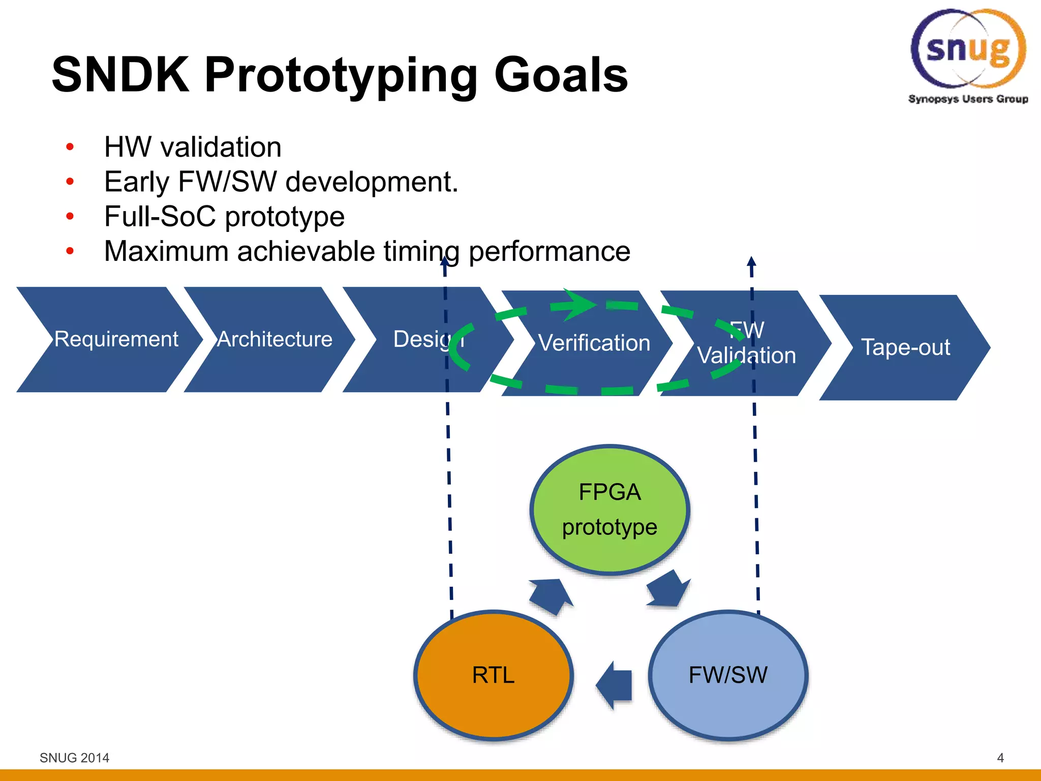
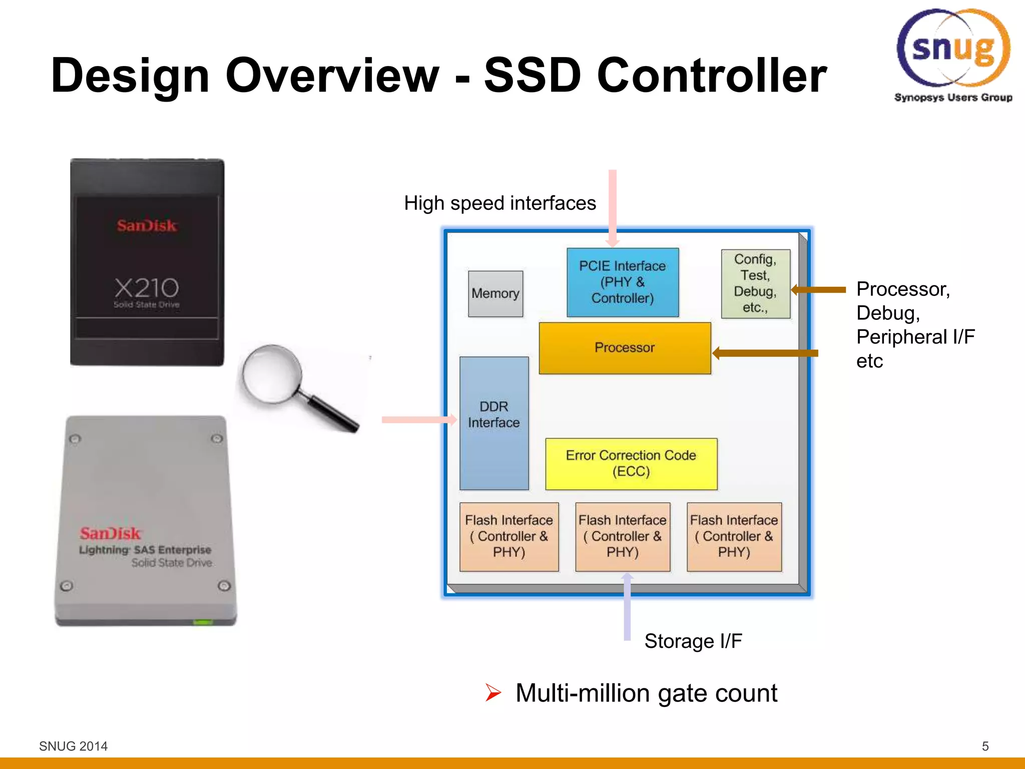
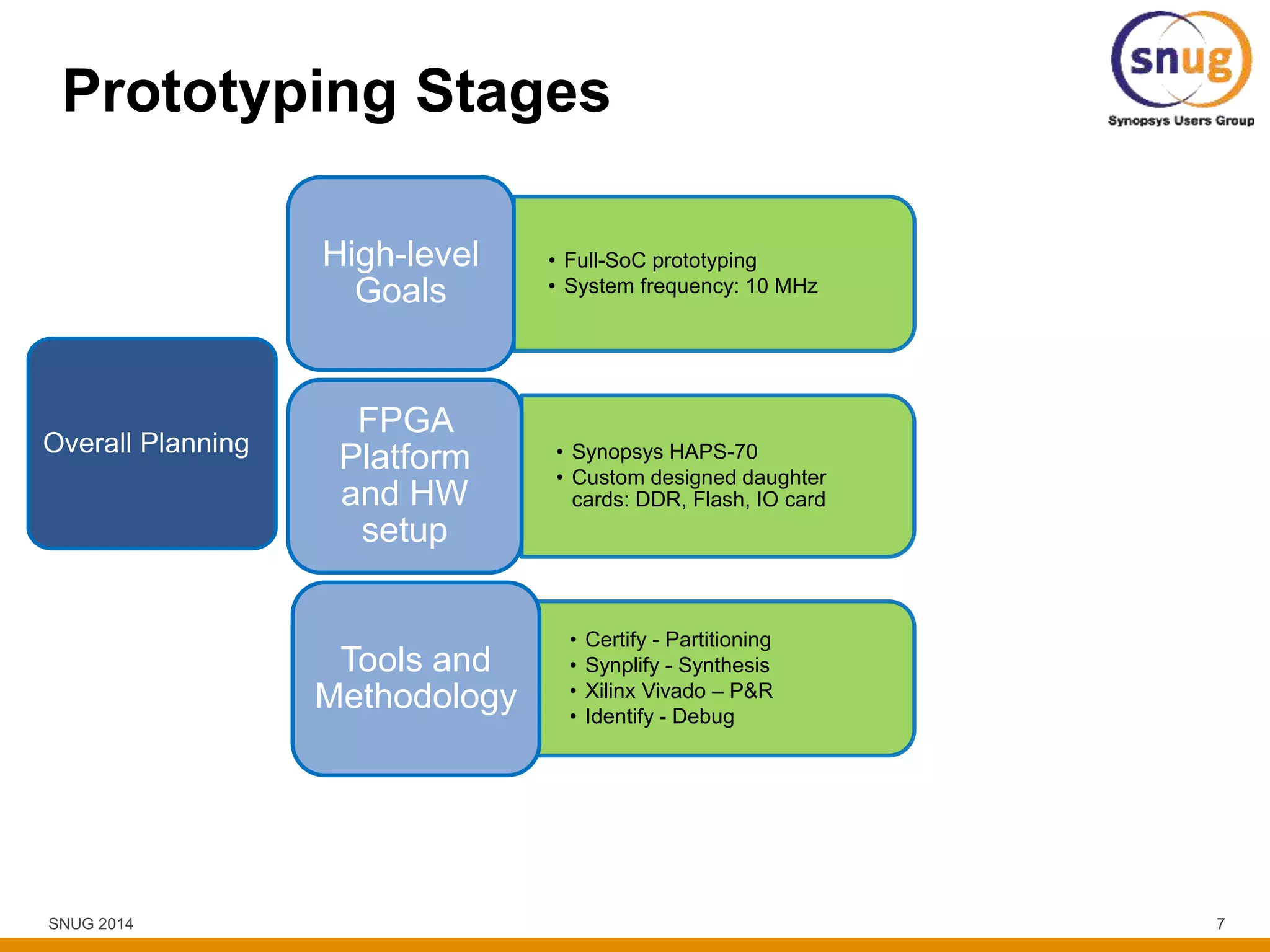
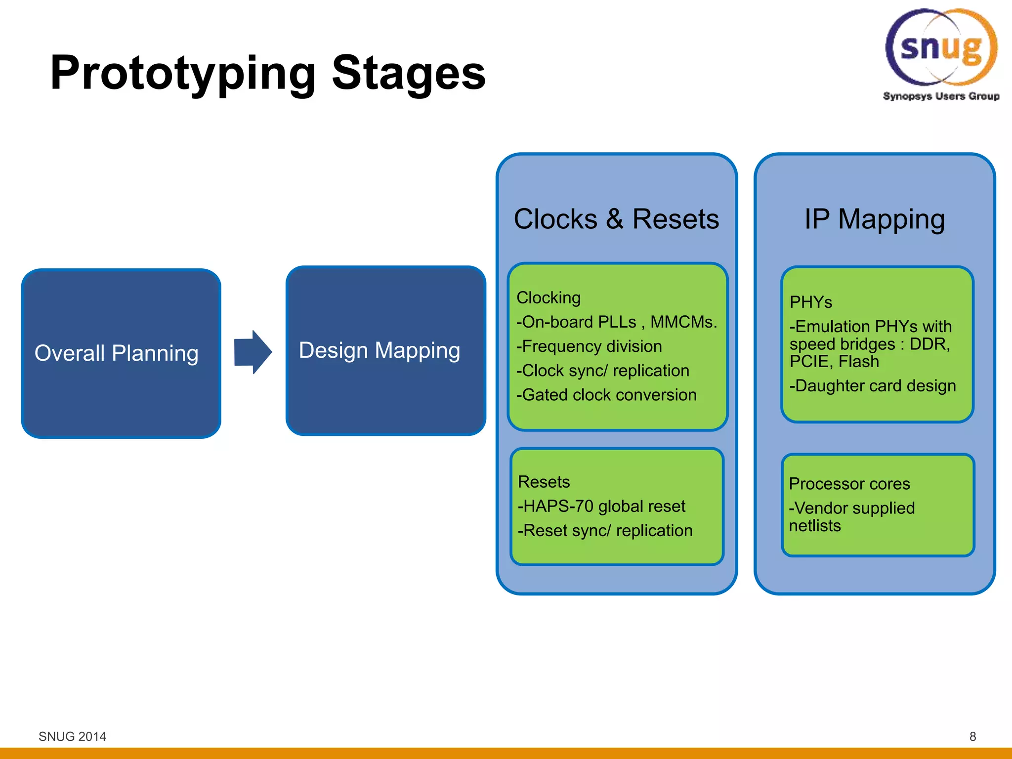
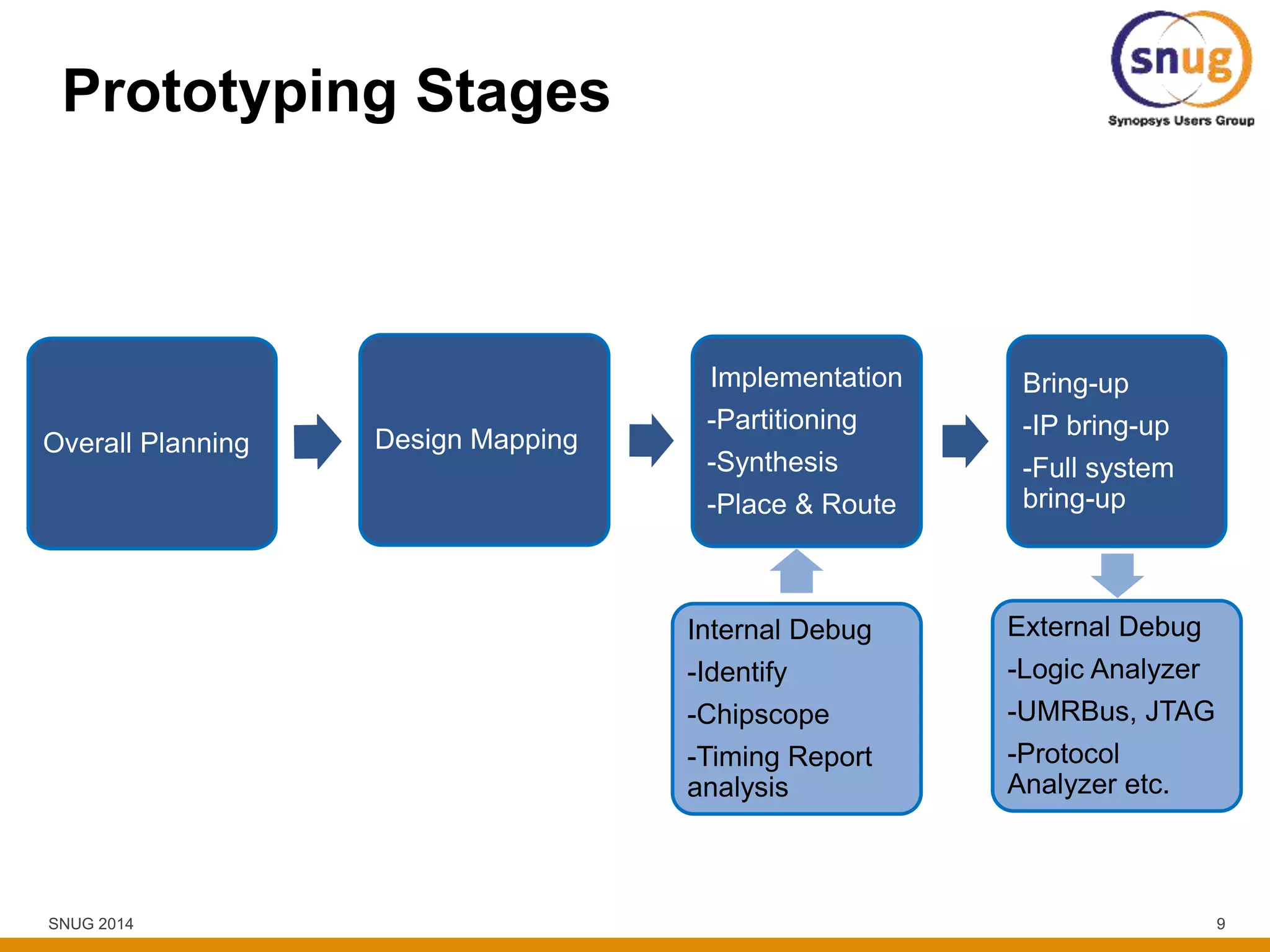
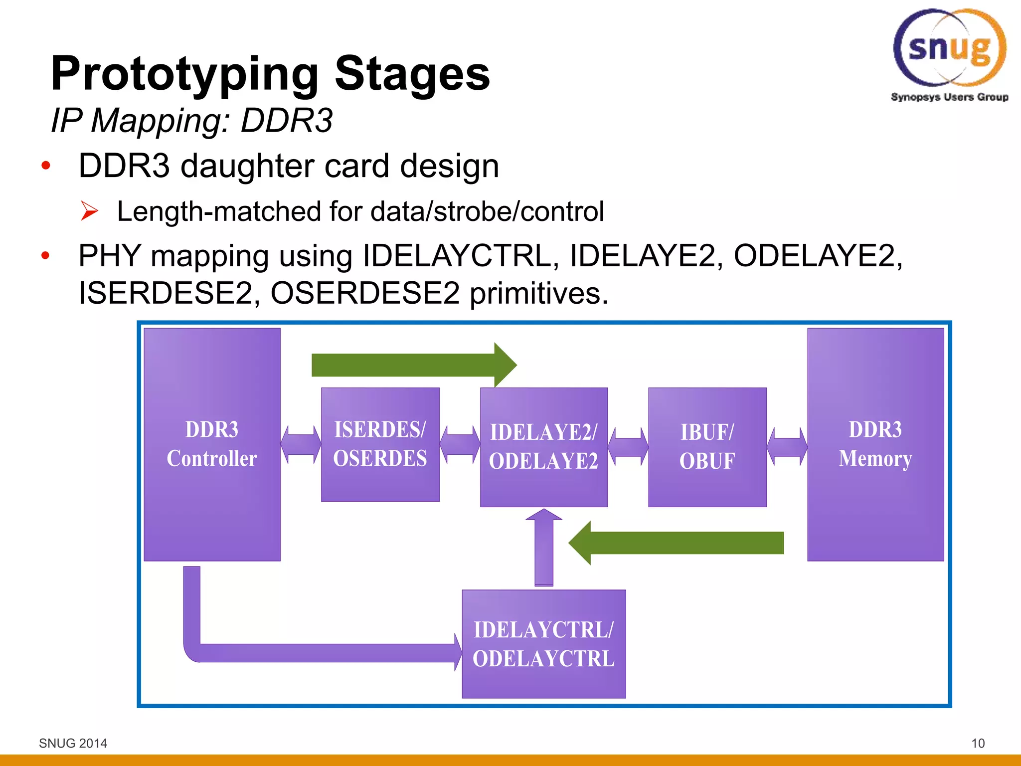
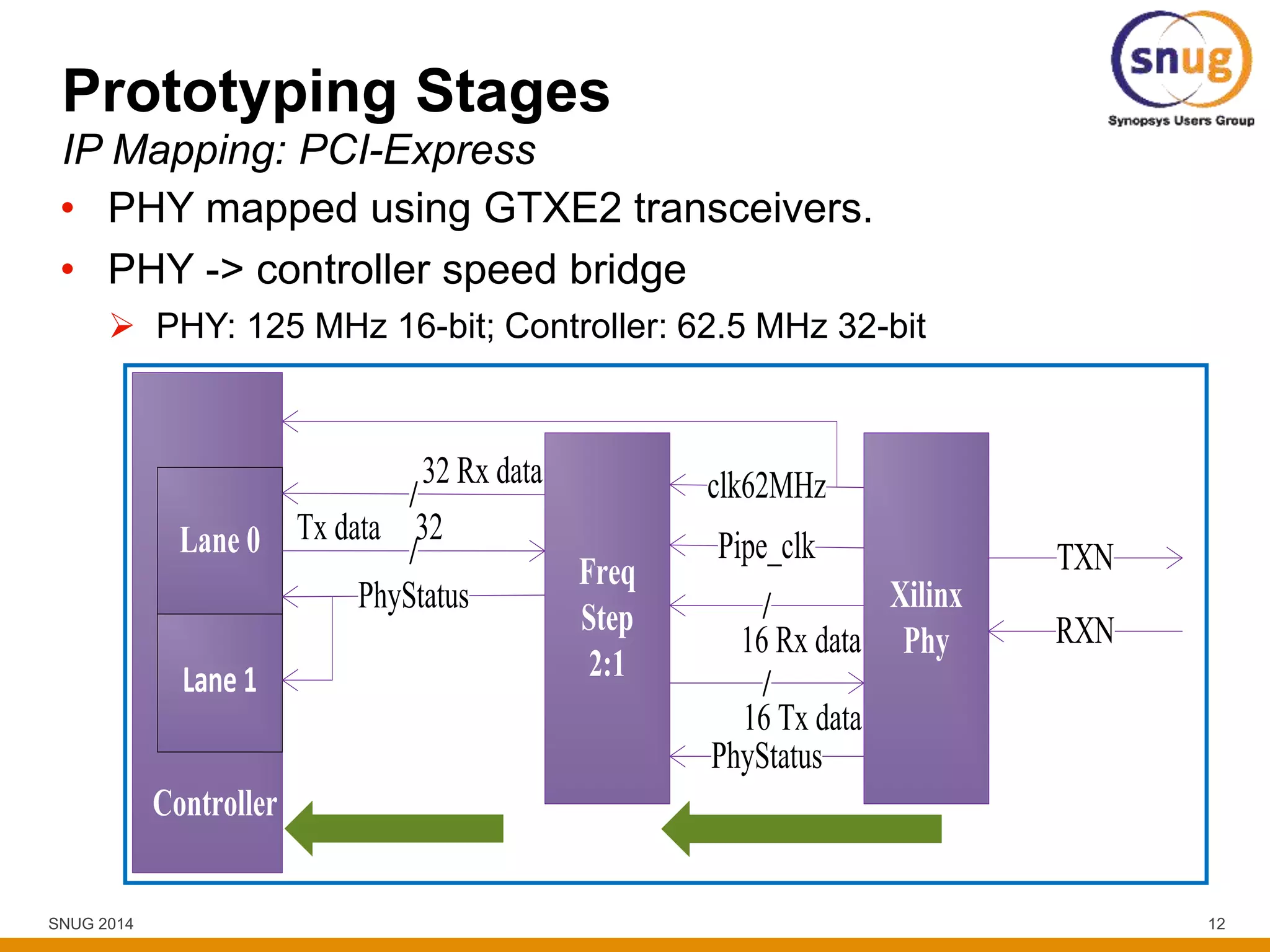
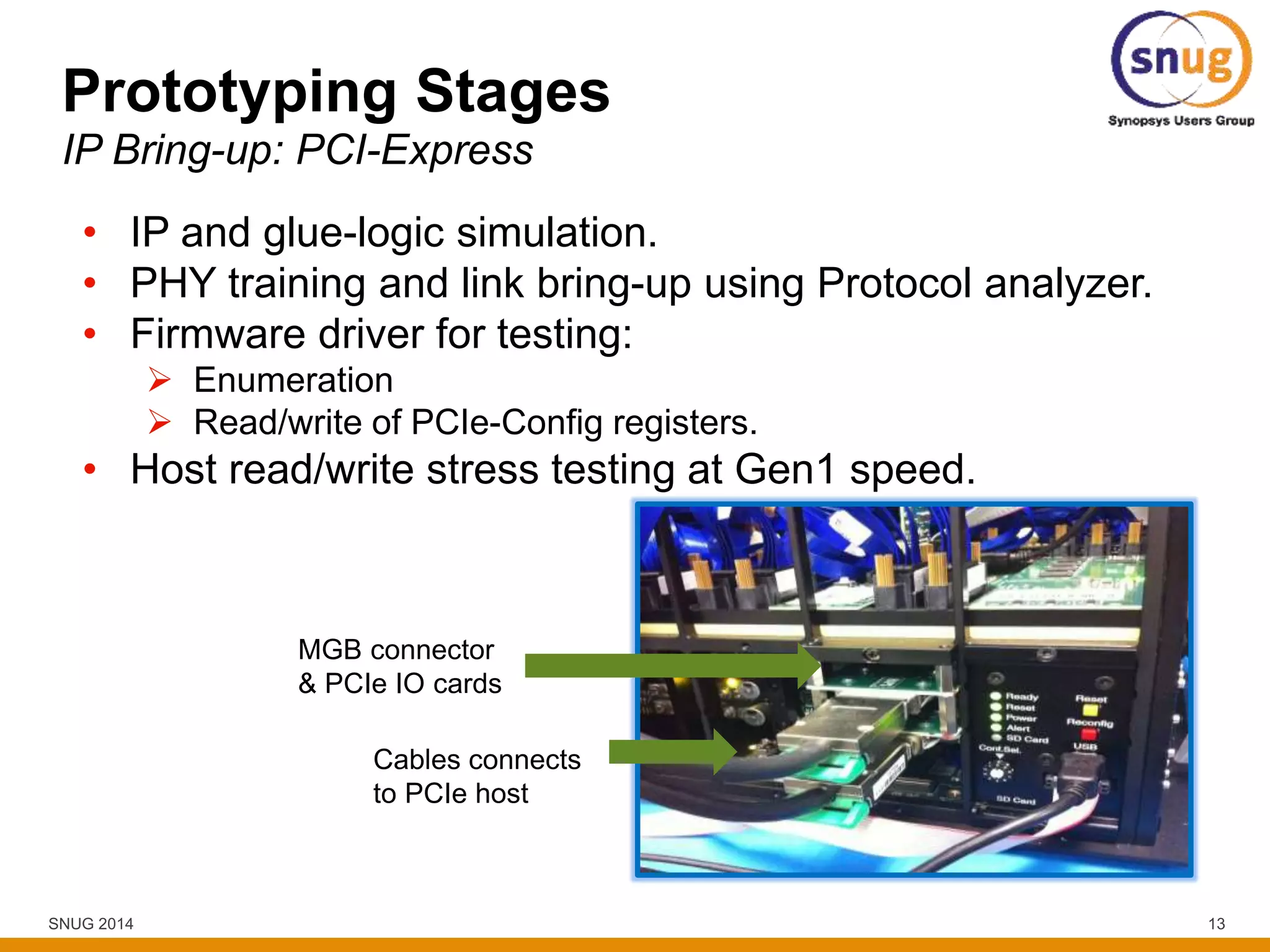
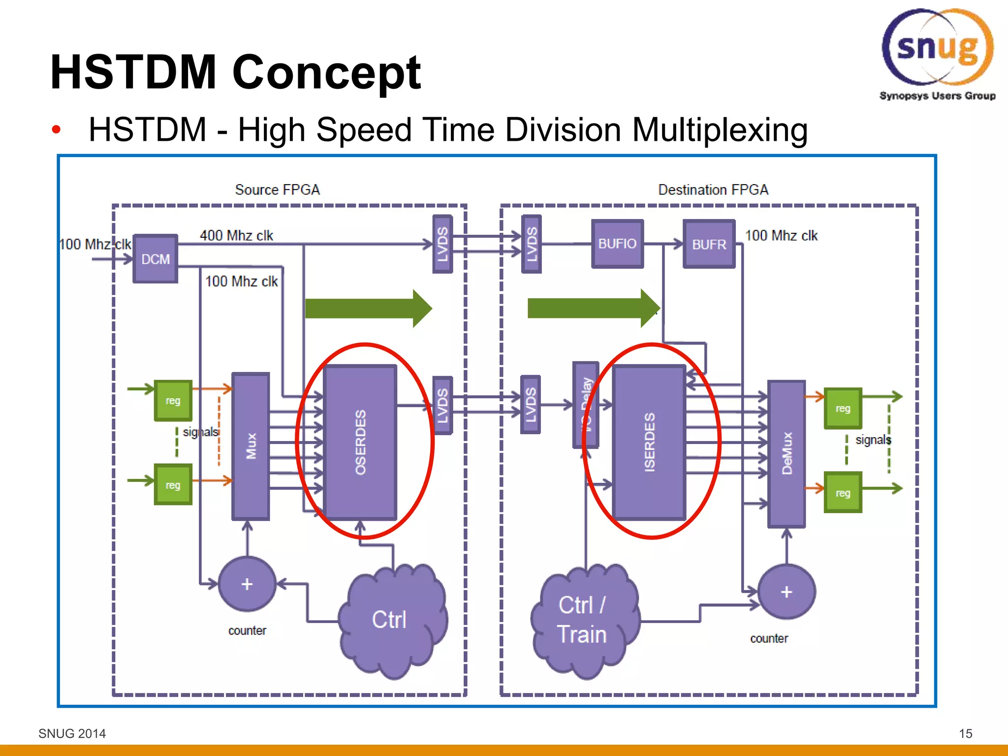
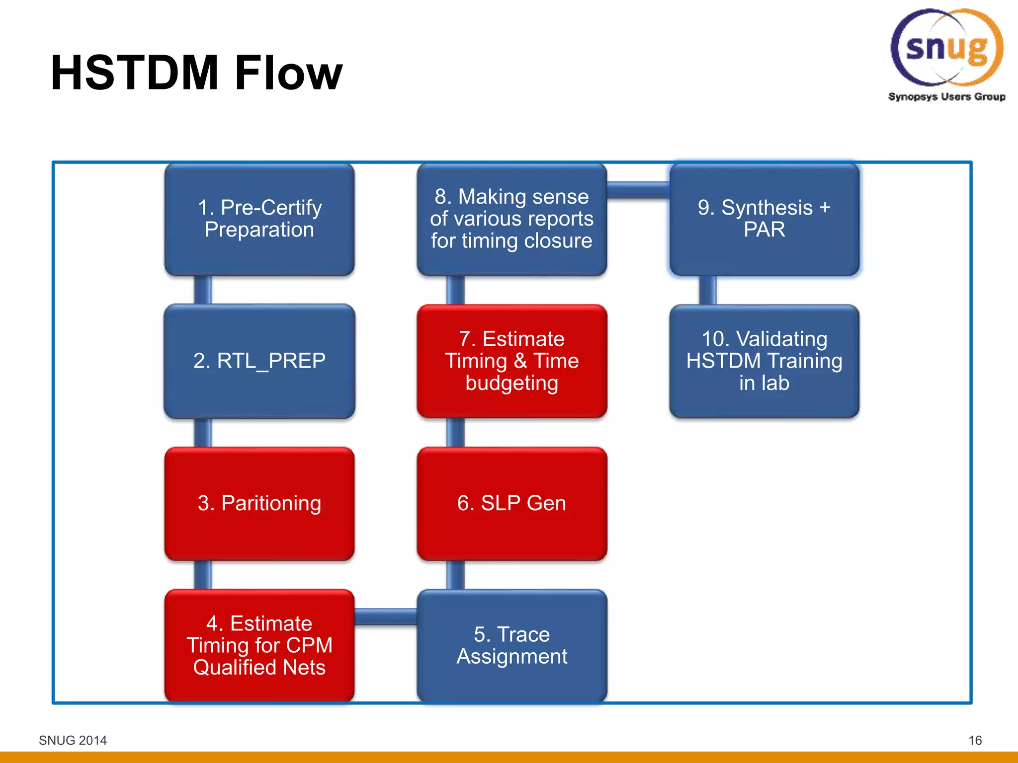
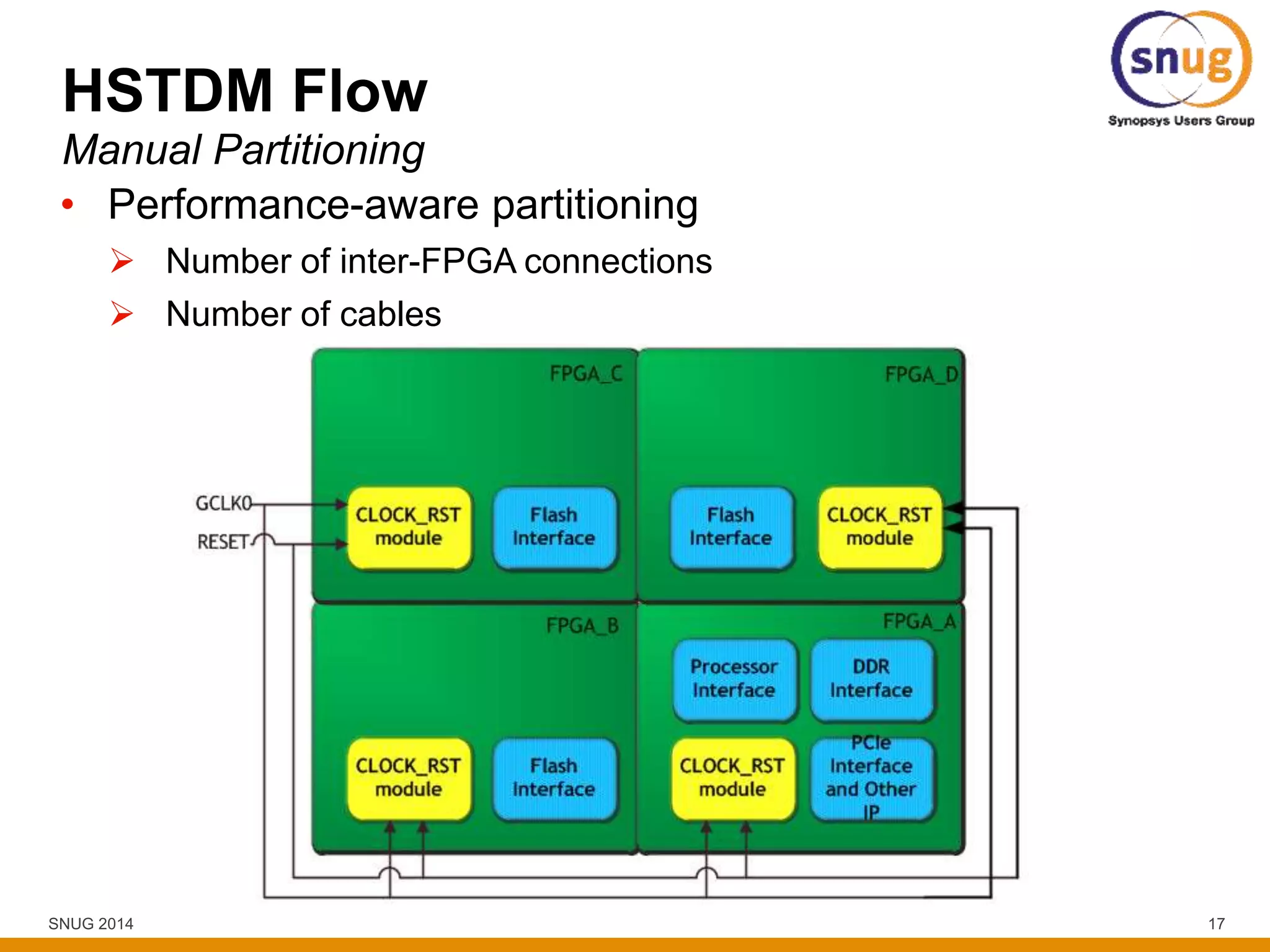
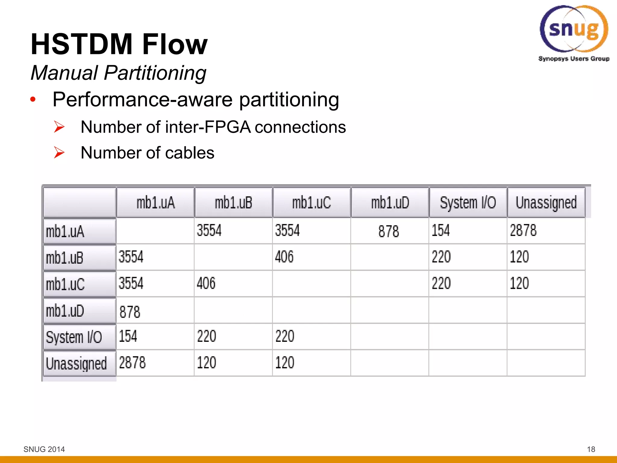
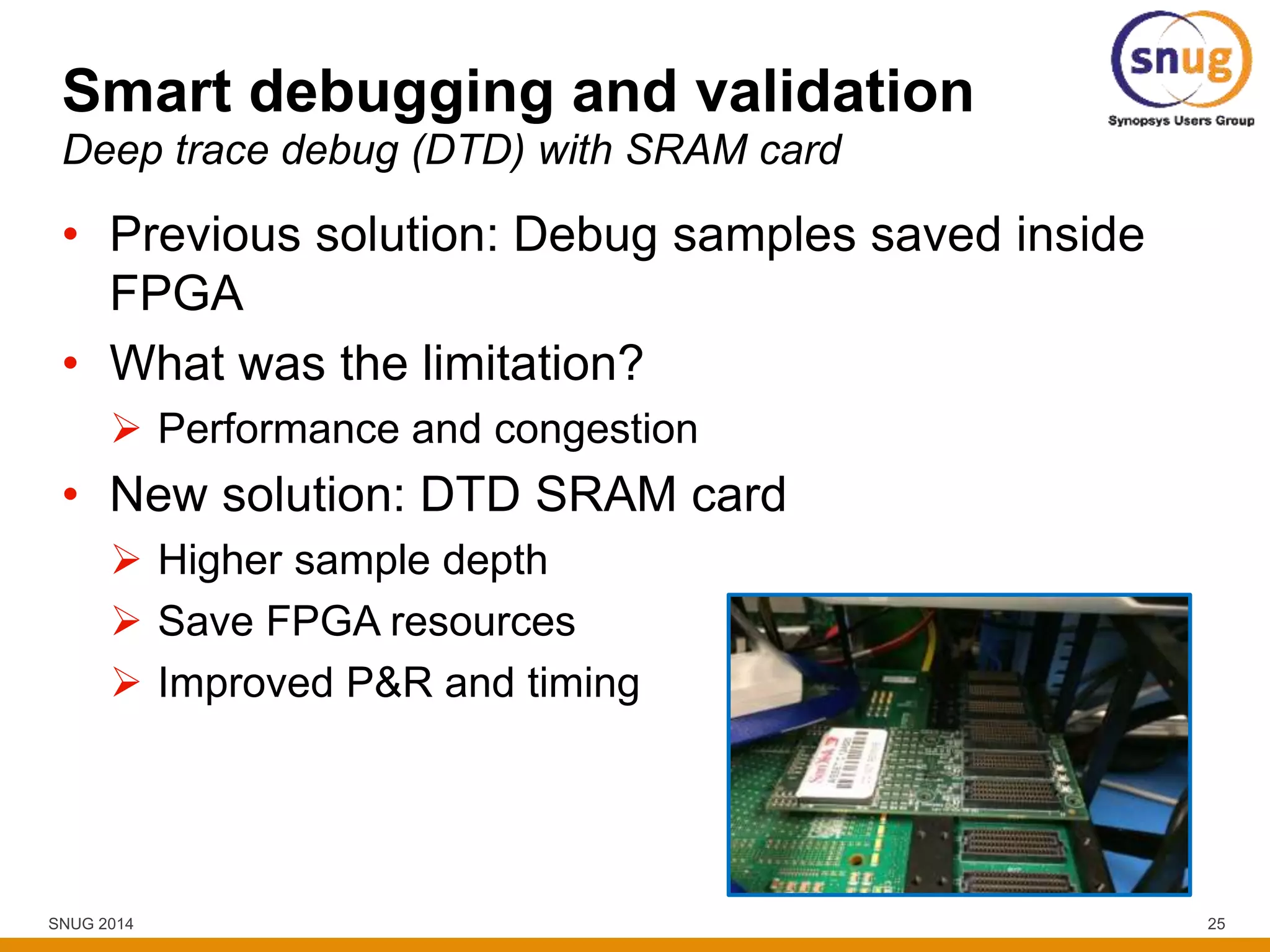
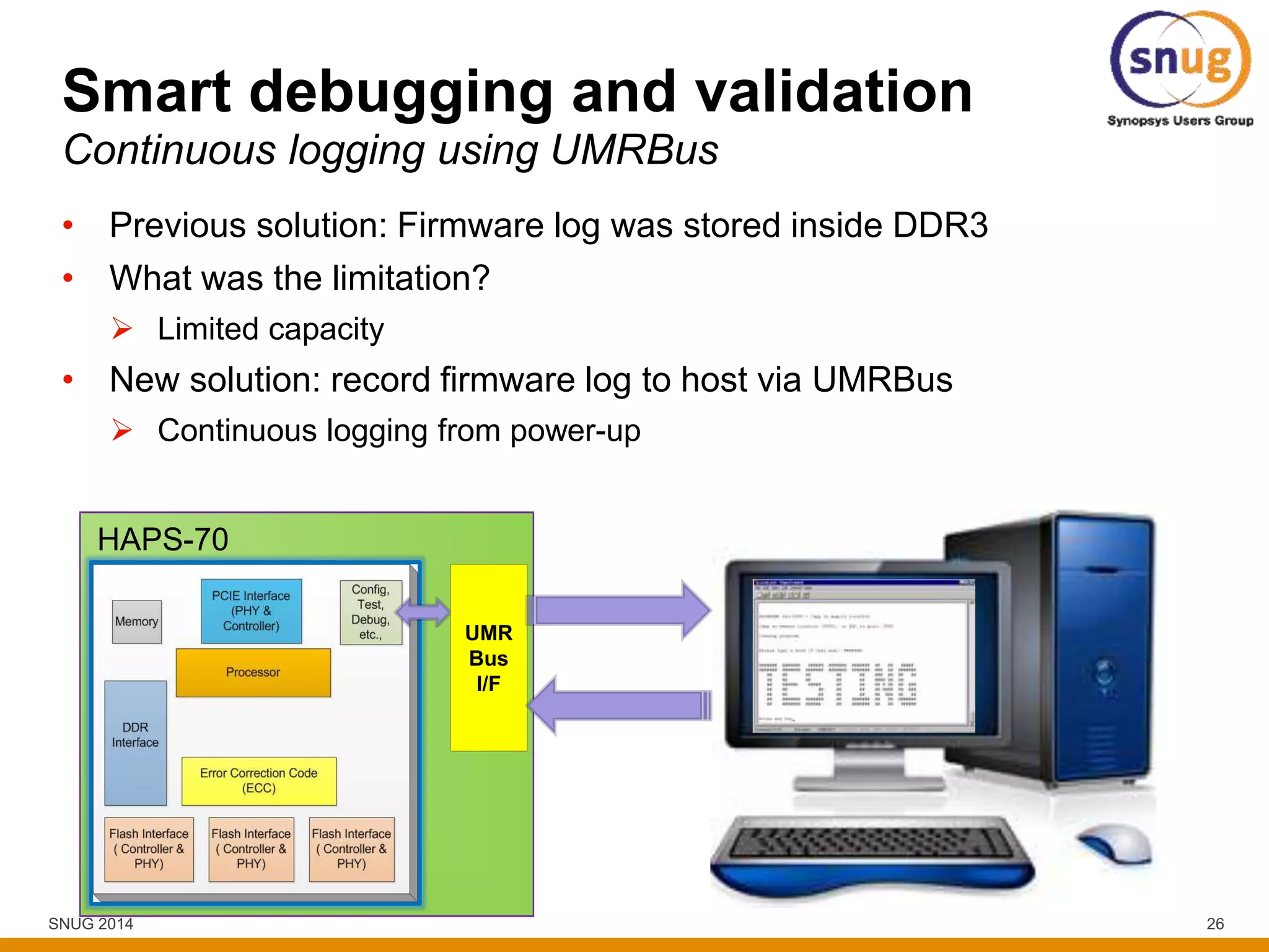
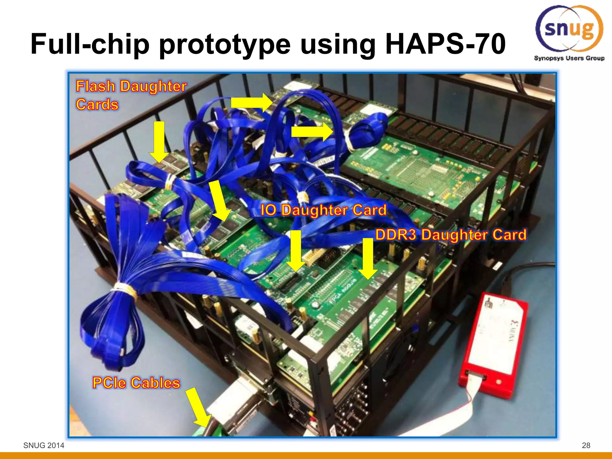
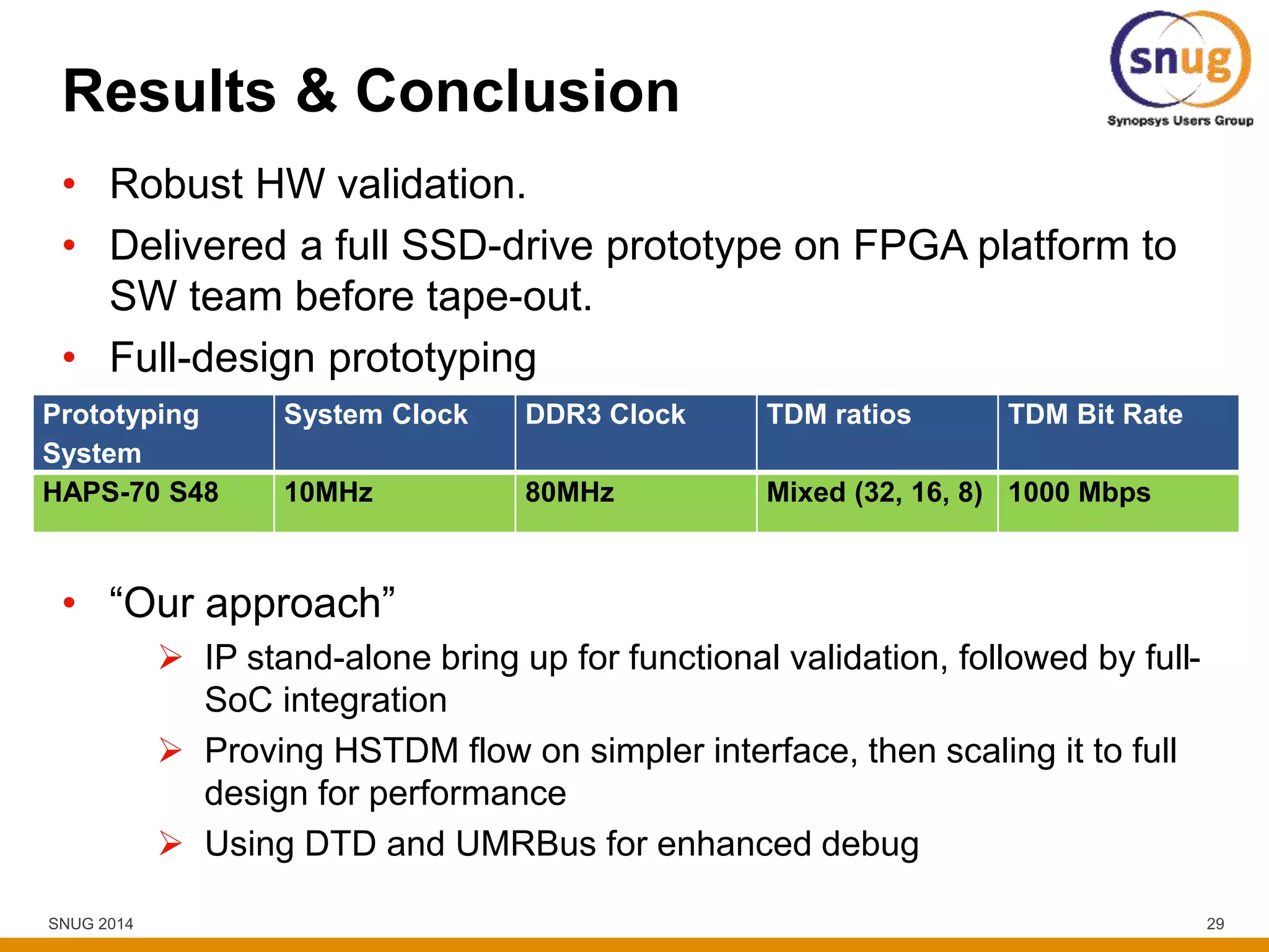
SNUG 2014 1
Achieving Maximum System Performance on
Multi-FPGA designs using
HAPS-70 FPGA Prototyping System
Jaseel Abdulla
Synopsys
May 16, 2014
Shanghai, China
SNUG 2014 2
Agenda
• SNDK Prototyping goals
• SoC Mapping to HAPS-70
• Leveraging HSTDM technology for maximizing system
performance
• Smart debugging
• Results & conclusion
• Q&A
SNUG 2014 3
SNDK Prototyping goals
SNUG 2014 4
SNDK Prototyping Goals
• HW validation
• Early FW/SW development.
• Full-SoC prototype
• Maximum achievable timing performance
Requirement Architecture Design Verification
FW
Validation Tape-out
FPGA
prototype
FW/SWRTL
SNUG 2014 5
Design Overview - SSD Controller
High speed interfaces
Processor,
Debug,
Peripheral I/F
etc
Storage I/F
 Multi-million gate count
SNUG 2014 6
SoC Mapping to HAPS-70
SNUG 2014 7
Prototyping Stages
Overall Planning
• Full-SoC prototyping
• System frequency: 10 MHz
High-level
Goals
• Synopsys HAPS-70
• Custom designed daughter
cards: DDR, Flash, IO card
FPGA
Platform
and HW
setup
• Certify - Partitioning
• Synplify - Synthesis
• Xilinx Vivado – P&R
• Identify - Debug
Tools and
Methodology
SNUG 2014 8
Prototyping Stages
Overall Planning Design Mapping
Clocks & Resets
Clocking
-On-board PLLs , MMCMs.
-Frequency division
-Clock sync/ replication
-Gated clock conversion
Resets
-HAPS-70 global reset
-Reset sync/ replication
IP Mapping
PHYs
-Emulation PHYs with
speed bridges : DDR,
PCIE, Flash
-Daughter card design
Processor cores
-Vendor supplied
netlists
SNUG 2014 9
Prototyping Stages
Overall Planning Design Mapping
Implementation
-Partitioning
-Synthesis
-Place & Route
Bring-up
-IP bring-up
-Full system
bring-up
Internal Debug
-Identify
-Chipscope
-Timing Report
analysis
External Debug
-Logic Analyzer
-UMRBus, JTAG
-Protocol
Analyzer etc.
SNUG 2014 10
ISERDES/
OSERDES
DDR3
Controller
IDELAYE2/
ODELAYE2
IBUF/
OBUF
IDELAYCTRL/
ODELAYCTRL
DDR3
Memory
Prototyping Stages
IP Mapping: DDR3
• DDR3 daughter card design
 Length-matched for data/strobe/control
• PHY mapping using IDELAYCTRL, IDELAYE2, ODELAYE2,
ISERDESE2, OSERDESE2 primitives.
SNUG 2014 11
Prototyping Stages
IP Bring-up: DDR3
• Simulation using DDR3 PHY emulation model
• DDR Init HW validation:
 Config registers
 Training
 Read/Write leveling
 Lab measurement of DQ/DQS alignment and skew
• Basic testing
• Firmware stress test of write-read-compare.
• Functional validation at 50 MHz.
• Successfully tested after full-SoC integration and
performance tuning at 80 MHz.
SNUG 2014 12
Prototyping Stages
IP Mapping: PCI-Express
• PHY mapped using GTXE2 transceivers.
• PHY -> controller speed bridge
 PHY: 125 MHz 16-bit; Controller: 62.5 MHz 32-bit
t
Lane 1
Lane 0
Freq
Step
2:1
Xilinx
Phy
Controller
/
PhyStatus
/
32 Rx data
Tx data 32 Pipe_clk
clk62MHz
/
PhyStatus
/
16 Rx data
16 Tx data
RXN
TXN
SNUG 2014 13
Prototyping Stages
IP Bring-up: PCI-Express
• IP and glue-logic simulation.
• PHY training and link bring-up using Protocol analyzer.
• Firmware driver for testing:
 Enumeration
 Read/write of PCIe-Config registers.
• Host read/write stress testing at Gen1 speed.
MGB connector
& PCIe IO cards
Cables connects
to PCIe host
SNUG 2014 14
Leveraging HSTDM technology for
maximizing System performance
SNUG 2014 15
HSTDM Concept
• HSTDM - High Speed Time Division Multiplexing
SNUG 2014 16
HSTDM Flow
1. Pre-Certify
Preparation
2. RTL_PREP
3. Paritioning
4. Estimate
Timing for CPM
Qualified Nets
5. Trace
Assignment
6. SLP Gen
7. Estimate
Timing & Time
budgeting
8. Making sense
of various reports
for timing closure
9. Synthesis +
PAR
10. Validating
HSTDM Training
in lab
SNUG 2014 17
HSTDM Flow
• Performance-aware partitioning
 Number of inter-FPGA connections
 Number of cables
Manual Partitioning
SNUG 2014 18
HSTDM Flow
• Performance-aware partitioning
 Number of inter-FPGA connections
 Number of cables
Manual Partitioning
SNUG 2014 19
HSTDM Flow
• Estimate timing on partitioned design.
• Select TDM Qualification criteria:
 All Nets
 Start and End @ Sequential
 End @ Sequential
 Start @ Sequential
• Report qualified TDM nets timing to get slack #s.
 Helps in excluding timing critical nets from TDM.
Using Timing estimate and Qualified TDM
SNUG 2014 20
HSTDM Flow
• Factor in User logic delay and TDM delay for grouping
nets into different TDM ratios.
• Don’t TDM critical nets like resets, feed-thru nets etc.
• Use mixed ratio TDM for better timing performance.
Grouping nets into TDM ratios
TDM version minimum
delay
freq with 10ns
user logic
freq with 20ns
user logic delay
HSTDM 4x2 21ns 32MHz 24MHz
HSTDM 6x2 33ns 23MHz 19MHz
HSTDM 8x2 40ns 20MHz 17MHz
HSTDM 16x2 55ns 15MHz 13MHz
HSTDM 32x2 75ns 12MHz 10.5MHz
HSTDM 64x2 117ns 7.9MHz 7.3MHz
HSTDM 128x2 197ns 5MHz 4.6MHz
SNUG 2014 21
HSTDM Flow
• Total cables = Num HSTDM cables + Num Non-HSTDM
cables
• Number of HT3 Cables for HSTDM = Total number of
Qualified Nets between 2 FPGAs / (Number of differential
pairs * HSTDM ratio)
• Example:
Cable calculation
FPGA _A FPGA _B3000 signals
Each cable needs a clock between FPGAs
24-2=22 : Usable diff-pair IOs
HSTDM ratio: 16
# of HSTDM cables required: 2700/(16*22)=8
SNUG 2014 22
HSTDM Flow
• SLPgen
 RTL based – mixed flow
 netlist based – srs flow
 time_est.srr – system level timing analysis
• Mixed mode useful for Identify instrumentation
• Run estimate timing
SLPgen and Timing estimate
SNUG 2014 23
HSTDM Flow
Log files and Timing Performance tuning process
RTL_PREP
design.srr
*_cck.rpt
PARTITION
TIMING_EST
cpm_time_est.
srr
qualified.txt
TRACE ASSIGN
&
SLPGEN
slpgen.srr
*_timing.sdc
HSTDM_
TIMING_EST
result_time
_est.srr
SNUG 2014 24
Smart Debugging
SNUG 2014 25
Smart debugging and validation
• Previous solution: Debug samples saved inside
FPGA
• What was the limitation?
 Performance and congestion
• New solution: DTD SRAM card
 Higher sample depth
 Save FPGA resources
 Improved P&R and timing
Deep trace debug (DTD) with SRAM card
SNUG 2014 26
HAPS-70
Smart debugging and validation
• Previous solution: Firmware log was stored inside DDR3
• What was the limitation?
 Limited capacity
• New solution: record firmware log to host via UMRBus
 Continuous logging from power-up
Continuous logging using UMRBus
UMR
Bus
I/F
SNUG 2014 27
Full-prototype lab set-up
SNUG 2014 28
Full-chip prototype using HAPS-70
SNUG 2014 29
• Robust HW validation.
• Delivered a full SSD-drive prototype on FPGA platform to
SW team before tape-out.
• Full-design prototyping
• “Our approach”
 IP stand-alone bring up for functional validation, followed by full-
SoC integration
 Proving HSTDM flow on simpler interface, then scaling it to full
design for performance
 Using DTD and UMRBus for enhanced debug
Results & Conclusion
Prototyping
System
System Clock DDR3 Clock TDM ratios TDM Bit Rate
HAPS-70 S48 10MHz 80MHz Mixed (32, 16, 8) 1000 Mbps
SNUG 2014 30
Thank You
SNUG 2014 31
Q&A

Snug 2014 China

  • 1.
    SNUG 2014 1 AchievingMaximum System Performance on Multi-FPGA designs using HAPS-70 FPGA Prototyping System Jaseel Abdulla Synopsys May 16, 2014 Shanghai, China
  • 2.
    SNUG 2014 2 Agenda •SNDK Prototyping goals • SoC Mapping to HAPS-70 • Leveraging HSTDM technology for maximizing system performance • Smart debugging • Results & conclusion • Q&A
  • 3.
    SNUG 2014 3 SNDKPrototyping goals
  • 4.
    SNUG 2014 4 SNDKPrototyping Goals • HW validation • Early FW/SW development. • Full-SoC prototype • Maximum achievable timing performance Requirement Architecture Design Verification FW Validation Tape-out FPGA prototype FW/SWRTL
  • 5.
    SNUG 2014 5 DesignOverview - SSD Controller High speed interfaces Processor, Debug, Peripheral I/F etc Storage I/F  Multi-million gate count
  • 6.
    SNUG 2014 6 SoCMapping to HAPS-70
  • 7.
    SNUG 2014 7 PrototypingStages Overall Planning • Full-SoC prototyping • System frequency: 10 MHz High-level Goals • Synopsys HAPS-70 • Custom designed daughter cards: DDR, Flash, IO card FPGA Platform and HW setup • Certify - Partitioning • Synplify - Synthesis • Xilinx Vivado – P&R • Identify - Debug Tools and Methodology
  • 8.
    SNUG 2014 8 PrototypingStages Overall Planning Design Mapping Clocks & Resets Clocking -On-board PLLs , MMCMs. -Frequency division -Clock sync/ replication -Gated clock conversion Resets -HAPS-70 global reset -Reset sync/ replication IP Mapping PHYs -Emulation PHYs with speed bridges : DDR, PCIE, Flash -Daughter card design Processor cores -Vendor supplied netlists
  • 9.
    SNUG 2014 9 PrototypingStages Overall Planning Design Mapping Implementation -Partitioning -Synthesis -Place & Route Bring-up -IP bring-up -Full system bring-up Internal Debug -Identify -Chipscope -Timing Report analysis External Debug -Logic Analyzer -UMRBus, JTAG -Protocol Analyzer etc.
  • 10.
    SNUG 2014 10 ISERDES/ OSERDES DDR3 Controller IDELAYE2/ ODELAYE2 IBUF/ OBUF IDELAYCTRL/ ODELAYCTRL DDR3 Memory PrototypingStages IP Mapping: DDR3 • DDR3 daughter card design  Length-matched for data/strobe/control • PHY mapping using IDELAYCTRL, IDELAYE2, ODELAYE2, ISERDESE2, OSERDESE2 primitives.
  • 11.
    SNUG 2014 11 PrototypingStages IP Bring-up: DDR3 • Simulation using DDR3 PHY emulation model • DDR Init HW validation:  Config registers  Training  Read/Write leveling  Lab measurement of DQ/DQS alignment and skew • Basic testing • Firmware stress test of write-read-compare. • Functional validation at 50 MHz. • Successfully tested after full-SoC integration and performance tuning at 80 MHz.
  • 12.
    SNUG 2014 12 PrototypingStages IP Mapping: PCI-Express • PHY mapped using GTXE2 transceivers. • PHY -> controller speed bridge  PHY: 125 MHz 16-bit; Controller: 62.5 MHz 32-bit t Lane 1 Lane 0 Freq Step 2:1 Xilinx Phy Controller / PhyStatus / 32 Rx data Tx data 32 Pipe_clk clk62MHz / PhyStatus / 16 Rx data 16 Tx data RXN TXN
  • 13.
    SNUG 2014 13 PrototypingStages IP Bring-up: PCI-Express • IP and glue-logic simulation. • PHY training and link bring-up using Protocol analyzer. • Firmware driver for testing:  Enumeration  Read/write of PCIe-Config registers. • Host read/write stress testing at Gen1 speed. MGB connector & PCIe IO cards Cables connects to PCIe host
  • 14.
    SNUG 2014 14 LeveragingHSTDM technology for maximizing System performance
  • 15.
    SNUG 2014 15 HSTDMConcept • HSTDM - High Speed Time Division Multiplexing
  • 16.
    SNUG 2014 16 HSTDMFlow 1. Pre-Certify Preparation 2. RTL_PREP 3. Paritioning 4. Estimate Timing for CPM Qualified Nets 5. Trace Assignment 6. SLP Gen 7. Estimate Timing & Time budgeting 8. Making sense of various reports for timing closure 9. Synthesis + PAR 10. Validating HSTDM Training in lab
  • 17.
    SNUG 2014 17 HSTDMFlow • Performance-aware partitioning  Number of inter-FPGA connections  Number of cables Manual Partitioning
  • 18.
    SNUG 2014 18 HSTDMFlow • Performance-aware partitioning  Number of inter-FPGA connections  Number of cables Manual Partitioning
  • 19.
    SNUG 2014 19 HSTDMFlow • Estimate timing on partitioned design. • Select TDM Qualification criteria:  All Nets  Start and End @ Sequential  End @ Sequential  Start @ Sequential • Report qualified TDM nets timing to get slack #s.  Helps in excluding timing critical nets from TDM. Using Timing estimate and Qualified TDM
  • 20.
    SNUG 2014 20 HSTDMFlow • Factor in User logic delay and TDM delay for grouping nets into different TDM ratios. • Don’t TDM critical nets like resets, feed-thru nets etc. • Use mixed ratio TDM for better timing performance. Grouping nets into TDM ratios TDM version minimum delay freq with 10ns user logic freq with 20ns user logic delay HSTDM 4x2 21ns 32MHz 24MHz HSTDM 6x2 33ns 23MHz 19MHz HSTDM 8x2 40ns 20MHz 17MHz HSTDM 16x2 55ns 15MHz 13MHz HSTDM 32x2 75ns 12MHz 10.5MHz HSTDM 64x2 117ns 7.9MHz 7.3MHz HSTDM 128x2 197ns 5MHz 4.6MHz
  • 21.
    SNUG 2014 21 HSTDMFlow • Total cables = Num HSTDM cables + Num Non-HSTDM cables • Number of HT3 Cables for HSTDM = Total number of Qualified Nets between 2 FPGAs / (Number of differential pairs * HSTDM ratio) • Example: Cable calculation FPGA _A FPGA _B3000 signals Each cable needs a clock between FPGAs 24-2=22 : Usable diff-pair IOs HSTDM ratio: 16 # of HSTDM cables required: 2700/(16*22)=8
  • 22.
    SNUG 2014 22 HSTDMFlow • SLPgen  RTL based – mixed flow  netlist based – srs flow  time_est.srr – system level timing analysis • Mixed mode useful for Identify instrumentation • Run estimate timing SLPgen and Timing estimate
  • 23.
    SNUG 2014 23 HSTDMFlow Log files and Timing Performance tuning process RTL_PREP design.srr *_cck.rpt PARTITION TIMING_EST cpm_time_est. srr qualified.txt TRACE ASSIGN & SLPGEN slpgen.srr *_timing.sdc HSTDM_ TIMING_EST result_time _est.srr
  • 24.
  • 25.
    SNUG 2014 25 Smartdebugging and validation • Previous solution: Debug samples saved inside FPGA • What was the limitation?  Performance and congestion • New solution: DTD SRAM card  Higher sample depth  Save FPGA resources  Improved P&R and timing Deep trace debug (DTD) with SRAM card
  • 26.
    SNUG 2014 26 HAPS-70 Smartdebugging and validation • Previous solution: Firmware log was stored inside DDR3 • What was the limitation?  Limited capacity • New solution: record firmware log to host via UMRBus  Continuous logging from power-up Continuous logging using UMRBus UMR Bus I/F
  • 27.
  • 28.
    SNUG 2014 28 Full-chipprototype using HAPS-70
  • 29.
    SNUG 2014 29 •Robust HW validation. • Delivered a full SSD-drive prototype on FPGA platform to SW team before tape-out. • Full-design prototyping • “Our approach”  IP stand-alone bring up for functional validation, followed by full- SoC integration  Proving HSTDM flow on simpler interface, then scaling it to full design for performance  Using DTD and UMRBus for enhanced debug Results & Conclusion Prototyping System System Clock DDR3 Clock TDM ratios TDM Bit Rate HAPS-70 S48 10MHz 80MHz Mixed (32, 16, 8) 1000 Mbps
  • 30.
  • 31.

Editor's Notes

  • #3 Set expectations here: Presenting an empirical model for best design practices for achieving desired system performances for a particular design.
  • #5 Talk about the diagram first
  • #6 Briefly dwell on the different if/s. Emphasize of the complexity of the SoC
  • #8 Spend more time design planning. Make the description crisp. Don’t get into too much details. End with the stand-alone IP bring-up “approach” SNDK took.
  • #9 Spend more time design planning. Make the description crisp. Don’t get into too much details. End with the stand-alone IP bring-up “approach” SNDK took.
  • #10 Spend more time design planning. Make the description crisp. Don’t get into too much details. End with the stand-alone IP bring-up “approach” SNDK took.
  • #11 IP bringup is the phase where rubber meets the road. Like all of you know DDR IP is ubiquitious in prsent day SoC designs. As part of early software development, DDR Is one of the first I/F which need to be functional. In this Project Synopsys DW IP is used and Core consultant automaticlly generates the PHY layer need for the IP. Here, CC uses deidcated Xilinx primitves like SERDES or DELAYCNTRLers to make the PHY Layer, In DDR, it is mandatory to have length matched trac for data strobe and control signals So here, during DDR3 training phase, controller determins the phase mismatch that exist in DQS to alligh data and strobe signals and based on that deleay primitives gets configured to match the delays. IDELAYCNTLers have various taps that controls delay of IDELAY/ODELAY blocks. The phase allighment information from training phase is stored in various registers of DDR3 control registers and used in subsequent data exchange. Training is reinitiated if any variation observed or requested by controller.
  • #16 Uses source synchronous multiplexing using diff clock and IO
  • #20 Estimate timing on partitioned srp netlist. estimate_timing –cpm designame.srp
  • #21 Estimate timing on partitioned srp netlist. estimate_timing –cpm designame.srp
  • #23 Estimate_timing design_slpgen.srp
  • #27 For the log file based debugging. Our previous solution is to store firmware log inside of DDR3 memory. So, what is the limitation here? Because we want to monitor our system performance changes for a long run, and that is very important information for the debug purpose. So we need a larger space to store the log file. But as you know, this DDR3 memory has limited capacity. Our new solution is to take advantage of UMRBus. This picture shows the concept. This is the host workstatoin and this is the FPGA prototyping system. Our whole design is prototyped onto this system. And the UMRBus is a thin-host bus interface in the middle. We run firmware on our design at FPGA system. And this FPGA system will keep generating log information. We run C-codes program at host workstation, and it will grab the logs from FPGA to host workstation through UMRBus. And save log files in the host workstation. So in this way, we can monitor our system performance changes during a long run. And that is the very important information we want to get during the pre-silicon validation.
  • #30 Reduced overall bring-up time; design change turn-around time, robust partitioning & HSTDM flow