(PRIYA) Rajgurunagar Call Girls Just Call 7001035870 [ Cash on Delivery ] Pun...
Unit 3.docx
1. UNIT - III
SEMICONDUCTOR DEVICES AND
APPLICATIONS
3.1 ATOM
Introduction
Atom is a Greek word and its means is particle, so atom is smallest particle of the
mater, which has properties of element. E.g. Iron, Al, cu, etc
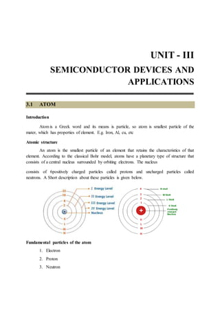
Atomic structure
An atom is the smallest particle of an element that retains the characteristics of that
element. According to the classical Bohr model, atoms have a planetary type of structure that
consists of a central nucleus surrounded by orbiting electrons. The nucleus
consists of 6positively charged particles called protons and uncharged particles called
neutrons. A Short description about these particles is given below.
Fundamental particles of the atom
1. Electron
2. Proton
3. Neutron
2. 3.2 Basic Electrical and Electronics Engineering
1. Electron
It also a fundamental particle of the atom. Electron is a particle which has negative
charge. The amount of the charge is -1.6x10⁻¹⁹ coulomb. Mass of electron is 9.11x10-
31kg or 0.00054859 a.m.u. Since atom has equal number of electrons and protons, they
have equal and opposite charges hence effect and atom becomes neutral. It is 1836
times lighter than proton. It is revolving around the nucleus.
2. Proton
Proton is a particle which has positive charge. It is inside the nucleus. The amount of
charge is 1.6x10⁻¹⁹ coulomb. The mass of proton is 1.67x10⁻²⁷ kg or 1.0072766 a.m.u.
It is 1836 times heavier than electron. The number of protons and electrons are equal
in an atom.
3. Neutron
Neutron is a neutral particle thus it has no any charge. Hence the name Neutron is
derived form the word neutral. It is heavier than electron. It mass is nearly equal to the
mass of proton that is equal to 1.6x10⁻²⁷kg or 1.0086654 a.m.u. It is 1842 times
heavier than electron.both the proton and neutron make the atomic mass of the atom. It
resits in site the nucleus.
ELECTRONIC CONFIGURATION
We know that electron is revolving around the nucleus in different position. These
positions are called energy levels or shell electrons are distributed among the shell according
to 2(N)2formula.
The number of electron in K shell 2N2 = 2(1)2 = 2
The number of electron in L shell 2N2 = 2(2)2 = 8
The number of electron in M shell 2N2 = 2(3)2 = 18 Etc, etc
The number of electron in the outer most shell is not distributed 2(N) 2 formula. The
outer most shell is called valance shell and the electron in it are called valence electron.
3. Semiconductor Devices and Applications 3.3
FOR EXAMPLE (CU)
ATOMIC NUMBER = 29
The number of electron in K Shell = 2(1) = 2
The number of electron in L shell = 2(2)2 = 8
The number of electron in M shell = 2(3)2 = 18
The number of electron in N shell = 1
ATOM ENERGY SHELLS OR LEVELS
"The orbit around the nucleus within which the electron rotate is called shells or
Energy levels."
Each discrete distance orbit from the nucleus corresponds to a certain energy level.
The electron which rotates in the lowest orbit has lowest energy level and in the outermost
orbit, electrons have higher energy levels. Hence energy levels increase as the distance from
the nucleus increases.
There are many shells around the nucleus which are arced as K, L, M; N, and so on.
K SHELL
The K Shell is the closest shell to the nucleus. It is stable with 2-electrons,
corresponding to the structure of Helium whose K Shell is filled with 2-electrons.
L SHELL
The L Shell is the second closest shell to the nucleus. It is stable with 8-elect- on,
Corresponding to the atomic structure of Neon whose L shell is filled with 8-electrons.
M SHELL
The I Shell is third closest shell to the nucleus. It is stable with 18 electrons
corresponding to the atomic structure of .Argon (Inert gas) whose M shell is filled by 18
electrons. Its electronic configuration is Shells
Shells Electrons
K 2
4. 3.4 Basic Electrical and Electronics Engineering
L 8
M 18
Total Electrons 28
Other shells which can take maximum electrons is shown by the table.
Shell Maximum Electrons Inert Gas
K 2 Helium
L 8 Neon
M 8 (upto Calcium) or 18 Argon
N 8, 18 or 32 Krypton
O 8 or 18 Xenon
P 8 or 18 Radon
Q 8 -----
For distribution of electrons in the shells, 2n2 rule is used where n is the number of
shell lives maximum electrons that can be placed in any shell
Valance Electron
"The electrons in an incomplete outermost orbit are called valance electrons."
Description
Valance electrons are less tightly bound to the atom than those closer to the nucleus.
This is because the force of attraction between the positively charged nucleus and the
negatively charged electron decreases with increasing distance from the nucleus. Electrons
with the highest energy levels exist in the outermost shell of an atom and are relatively loosely
bound to the atom. This outermost shell is known as the valance shell and electrons in this
shell are called valance electrons.
A completed outermost shell has valance of zero. copper has valance of 1 because one
electron is in outer shell after completing its inner shells. Similarly carbon has a valance
of 4 and all the inert gasses such as have zero valance.
5. Semiconductor Devices and Applications 3.5
3.2 ENERGYBAND
When no of atoms is combining then the whole energy levels are dividing in sub
energy levels and become overlapped. They make a band, which is called energy band.
Remember that the energy of free electron is changing continuously.
In a solid there are three type of energy band.
1. Filled band
As clear from its name it is that type of band, which is near to the nucleus, and it is
completely full with electron. In that type of band there are no free electron.
2. Valance band
The last band of the atom is called valance band and the electron of that band is called
valance electron. When valance electron gain some energy then they leave that band
and cross the energy gap which is also called forbidden energy gap and goes to
conduction band then current flow starts from this material. The energy of the valance
electron is more as compare to filled band.
3. Conduction band
When free electrons are escape from its permanent atom from to conduction band and
such process is called conduction. The electron of such band is called free electron.
a. Insulator
Insulator is that material in which current dose not flows easily e.g. Wood, paper,
plastic, oil, mica etc The reason for insulation is the wide gape between the valance
band and conduction band. A large amount of energy is required to shift electrons
from the valence band in to the conduction band.
b. Conductor
Conductor is those materials in which current flows easily. For example silver, cu and
aluminum etc The reason for the conduction the absence of forbidden between the
6. 3.6 Basic Electrical and Electronics Engineering
absence of forbidden band, so very small amount of energy is required for the flow of
electric current. There are many free electrons in the conducting materials.
c. Semi conductor
Semi conductor are those material which has the conduction property in between
conductor and insulator. It means semi conductor do not allow the free electron to flow
as conductor. In the same way semi conductor doesn’t block the current as insulator.
For example silicon, boron, carbon etc. The reason for such type of conductor is the
small gap between the valence band and conduction band. Semi conductors have
comparatively less free electron than the conductor.
Types of semiconductor
1.Intrinsic Semiconductors
2.Extrinsic semiconductors
3.3 INTRINSIC SEMICONDUCTOR
An intrinsic semiconductor, also called an undoped semiconductor or i-type
semiconductor, is a pure semiconductor without any significant dopant species present. The
number of charge carriers is therefore determined by the properties of the material itself
instead of the amount of impurities. In intrinsic semiconductors the number of
excited electrons and the number of holes are equal: n = p.
The electrical conductivity of intrinsic semiconductors can be due to crystallographic
defects or electron excitation. In an intrinsic semiconductor the number of electrons in
the conduction band is equal to the number of holes in the valence band. An example
is Helium 0.8Cd 0.2Te at room temperature.
7. Semiconductor Devices and Applications 3.7
An indirect band gap intrinsic semiconductor is one in which the maximum energy of
the valence band occurs at a different k (k-space wave vector) than the minimum energy of
the conduction band. Examples include silicon and germanium. A direct band gap intrinsic
semiconductor is one where the maximum energy of the valence band occurs at the same k as
the minimum energy of the conduction band. Examples include gallium arsenide.
A silicon crystal is different from an insulator because at any temperature above
absolute zero temperature, there is a finite probability that an electron in the lattice will be
knocked loose from its position, leaving behind an electron deficiency called a "hole".
If a voltage is applied, then both the electron and the hole can contribute to a small
current flow.
The conductivity of a semiconductor can be modeled in terms of the band theory of
solids. The band model of a semiconductor suggests that at ordinary temperatures there is a
finite possibility that electrons can reach the conduction band and contribute to electrical
conduction.
The term intrinsic here distinguishes between the properties of pure "intrinsic" silicon and the
dramatically different properties of doped n-type or p-type semiconductors.
Electrons and Holes
In an intrinsic semiconductor such as silicon at temperatures above absolute zero, there
will be some electrons which are excited across the band gap into the conduction band and
which can support current flow. When the electron in pure silicon crosses the gap, it leaves
behind an electron vacancy or "hole" in the regular silicon lattice. Under the influence of an
external voltage, both the electron and the hole can move across the material. In an n-type
semiconductor, the dopant contributes extra electrons, dramatically increasing the
conductivity. In a p-type semiconductor, the dopant produces extra vacancies or holes, which
likewise increase the conductivity. It is however the behavior of the p-n junction which is the
key to the enormous variety of solid-state electronic devices.
Semiconductor Current
The current which will flow in an intrinsic semiconductor consists of both electron and
hole current. That is, the electrons which have been freed from their lattice positions into the
conduction band can move through the material. In addition, other electrons can hop between
lattice positions to fill the vacancies left by the free electrons. This additional mechanism is
called hole conduction because it is as if the holes are migrating across the material in the
direction opposite to the free electron movement. The current flow in an intrinsic
semiconductor is influenced by the density of energy states which in turn influences
the electron density in the conduction band. This current is highly temperature dependent.
8. 3.8 Basic Electrical and Electronics Engineering
3.4 EXTRINSIC SEMICONDUCTOR
An extrinsic semiconductor is a semiconductor that has been doped, that is, into
which a doping agent has been introduced, giving it different electrical properties than
the intrinsic (pure) semiconductor.
Doping involves adding dopant atoms to an intrinsic semiconductor, which changes
the electron and hole carrier concentrations of the semiconductor at thermal equilibrium.
Dominant carrier concentrations in an extrinsic semiconductor classify it as either an n-type or
p-type semiconductor. The electrical properties of extrinsic semiconductors make them
essential components of many electronic devices.
Semiconductor doping
Semiconductor doping is the process that changes an intrinsic semiconductor to an
extrinsic semiconductor. During doping, impure atoms are introduced to an intrinsic
semiconductor. Impurity atoms are atoms of a different element than the atoms of the intrinsic
semiconductor. Impurity atoms act as either donors or acceptors to the intrinsic
semiconductor, changing the electron and hole concentrations of the semiconductor. Impurity
atoms are classified as donor or acceptor atoms based on the effect they have on the intrinsic
semiconductor.
Donor impurity atoms have more valence electrons than the atoms they replace in the
intrinsic semiconductor lattice. Donor impurities "donate" their extra valence electrons to a
semiconductor's conduction band, providing excess electrons to the intrinsic semiconductor.
Excess electrons increase the electron carrier concentration (n0) of the semiconductor, making
it n-type.
Acceptor impurity atoms have fewer valence electrons than the atoms they replace in
the intrinsic semiconductor. They "accept" electrons from the semiconductor's valence band.
This provides excess holes to the intrinsic semiconductor. Excess holes increase the hole
carrier concentration (p0) of the semiconductor, creating a p-type semiconductor.
9. Semiconductor Devices and Applications 3.9
Semiconductors and dopant atoms are defined by the column of the periodic in which
they fall. The column definition of the semiconductor determines how many valence electrons
its atoms have and whether dopant atoms act as the semiconductor's donors or acceptors.
Group IV semiconductors use group V atoms as donors and group III atoms as
acceptors.
Group III-V semiconductors, the compound semiconductors, use group VI atoms as
donors and group II atoms as acceptors. Group III-V semiconductors can also use group
IV atoms as either donors or acceptors. When a group IV atom replaces the group III element
in the semiconductor lattice, the group IV atom acts as a donor. Conversely, when a group IV
atom replaces the group V element, the group IV atom acts as an acceptor. Group IV atoms
can act as both donors and acceptors; therefore, they are known as amphoteric impurities.
Intrinsic
semiconductor
Donor atoms Acceptor atoms
Group IV
semicondu
ctors
Silicon, Germanium Phosphorus, Arsenic Boron, Aluminium
Group III-
V
semicondu
ctors
Aluminum
phosphide, Aluminum
arsenide, Gallium
arsenide, Gallium
nitride
Selenium, Tellurium,
Silicon,Germanium
Beryllium, Zinc, Cadmium, Silicon
Germanium
The two types of extrinsic semiconductor
N-type semiconductors
Fig. Band structure of an n-type semiconductor. Dark circles in the conduction band
are electrons and light circles in the valence band are holes. The image shows that the
electrons are the majority charge carrier.
Extrinsic semiconductors with a larger electron concentration than hole concentration
are known as n-type semiconductors. The phrase 'n-type' comes from the negative charge of
the electron. In n-type semiconductors, electrons are the majority carriers and holes are
the minority carriers. N-type semiconductors are created by doping an intrinsic semiconductor
with donor impurities (or doping a p-type semiconductor as done in the making of CMOS
chips). A common dopant for n-type semiconductors is Phosphorous. In an n-type
semiconductor, the Fermi energy level is greater than that of the intrinsic semiconductor and
lies closer to the conduction band than the valence band.
10. 3.10 Basic Electrical and Electronics Engineering
P-type semiconductors
Fig. Band structure of a p-type semiconductor. Dark circles in the conduction band are
electrons and light circles in the valence band are holes. The image shows that the holes are
the majority charge carrier
As opposed to n-type semiconductors, p-type semiconductors have a larger hole
concentration than electron concentration. The phrase 'p-type' refers to the positive charge of
the hole. In p-type semiconductors, holes are the majority carriers and electrons are the
minority carriers. P-type semiconductors are created by doping an intrinsic semiconductor
with acceptor impurities (or doping a n-type semiconductor). A common P-type dopant is
Boron. P-type semiconductors have Fermi energy levels below the intrinsic Fermi energy
level. The Fermi energy level lies closer to the valence band than the conduction band in a p-
type semiconductor.
Use of extrinsic semiconductors
Extrinsic semiconductors are components of many common electrical devices. A
semiconductor diode (devices that allow current in only one direction) consists of p-type and
n-type semiconductors placed in junction with one another. Currently, most semiconductor
diodes use doped silicon or germanium.
Transistors (devices that enable current switching) also make use of extrinsic
semiconductors. Bipolar junction transistors (BJT) are one type of transistor. The most
common BJTs are NPN and PNP type. NPN transistors have two layers of n-type
semiconductors sandwiching a p-type semiconductor. PNP transistors have two layers of p-
type semiconductors sandwiching an n-type semiconductor.
Field-effect transistors (FET) are another type of transistor implementing extrinsic
semiconductors. As opposed to BJTs, they are unipolar and considered either N-channel or P-
channel. FETs are broken into two families, junction gate FET (JFET) and insulated gate FET
(IGFET).
Other devices implementing the extrinsic semiconductor:
1. Lasers
2. Solar cells
3. Photodetectors
4. Light-emitting diodes
5. Thyristors
11. Semiconductor Devices and Applications 3.11
INTRINSIC
SEMICONDUCTORS
EXTRINSIC SEMICONDUCTORS
It is pure semi-conducting material
and no impurity atoms are added to
it.
It is prepared by doping a small quantity of
impurity atoms to the pure semi-conducting
material.
Examples: crystalline forms of pure
silicon and germanium.
Examples: silicon “Si” and germanium
“Ge” crystals with impurity atoms of As,
Sb, P etc. or In B, Aℓ etc.
The number of free electrons in the
conduction band and the no. of
holes in valence band is exactly
equal and very small indeed.
The number of free electrons and holes is
never equal. There is excess of electrons in
n-type semi-conductors and excess of holes
in p-type semi-conductors.
Its electrical conductivity is low. Its electrical conductivity is high.
Its electrical conductivity is a
function of temperature alone.
Its electrical conductivity depends upon the
temperature as well as on the quantity of
impurity atoms doped the structure.
3.5 THEORY OF PN JUNCTION
The Junction Diode
This achieved without any external voltage being applied to the actual PN junction
resulting in the junction being in a state of equilibrium. However, if we were to make
electrical connections at the ends of both the N-type and the P-type materials and then connect
them to a battery source, an additional energy source now exists to overcome the barrier
resulting in free charges being able to cross the depletion region from one side to the other.
The behaviour of the PN junction with regards to the potential barrier width produces an
asymmetrical conducting two terminal device, better known as the Junction Diode.
A diode is one of the simplest semiconductor devices, which has the characteristic of
passing current in one direction only. However, unlike a resistor, a diode does not behave
linearly with respect to the applied voltage as the diode has an exponential I-V relationship
and therefore we cannot described its operation by simply using an equation such as Ohm's
law.
If a suitable positive voltage (forward bias) is applied between the two ends of the PN
junction, it can supply free electrons and holes with the extra energy they require to cross the
12. 3.12 Basic Electrical and Electronics Engineering
junction as the width of the depletion layer around the PN junction is decreased. By applying
a negative voltage (reverse bias) results in the free charges being pulled away from the
junction resulting in the depletion layer width being increased. This has the effect of
increasing or decreasing the effective resistance of the junction itself allowing or blocking
current flow through the diode.
Then the depletion layer widens with an increase in the application of a reverse
voltage and narrows with an increase in the application of a forward voltage. This is due to the
differences in the electrical properties on the two sides of the PN junction resulting in physical
changes taking place. One of the results produces rectification as seen in the PN junction
diodes static I-V (current-voltage) characteristics. Rectification is shown by an asymmetrical
current flow when the polarity of bias voltage is altered as shown below.
3.5.1 Junction Diode Symbol and Static I-V Characteristics.
But before we can use the PN junction as a practical device or as a rectifying device
we need to firstly bias the junction, ie connect a voltage potential across it. On the voltage
axis above, "Reverse Bias" refers to an external voltage potential which increases the potential
barrier. An external voltage which decreases the potential barrier is said to act in the "Forward
Bias" direction.
There are two operating regions and three possible "biasing" conditions for the
standard Junction Diode and these are:
1. Zero Bias - No external voltage potential is applied to the PN-junction.
2. Reverse Bias - The voltage potential is connected negative, (-ve) to the P-type
material
and positive, (+ve) to the N-type material across the diode which has the effect of
Increasing the PN-junction width.
13. Semiconductor Devices and Applications 3.13
3. Forward Bias - The voltage potential is connected positive, (+ve) to the P-type
material and negative, (-ve) to the N-type material across the diode which has the
effect of Decreasing the PN-junction width.
Zero Biased Junction Diode
When a diode is connected in a Zero Bias condition, no external potential energy is
applied to the PN junction. However if the diodes terminals are shorted together, a few holes
(majority carriers) in the P-type material with enough energy to overcome the potential barrier
will move across the junction against this barrier potential. This is known as the "Forward
Current" and is referenced as IF
Likewise, holes generated in the N-type material (minority carriers), find this situation
favourable and move across the junction in the opposite direction. This is known as the
"Reverse Current" and is referenced as IR. This transfer of electrons and holes back and forth
across the PN junction is known as diffusion, as shown below.
3.5.2 Zero Biased Junction Diode
The potential barrier that now exists discourages the diffusion of any more majority
carriers across the junction. However, the potential barrier helps minority carriers (few free
electrons in the P-region and few holes in the N-region) to drift across the junction. Then an
"Equilibrium" or balance will be established when the majority carriers are equal and both
moving in opposite directions, so that the net result is zero current flowing in the circuit.
When this occurs the junction is said to be in a state of "Dynamic Equilibrium".
The minority carriers are constantly generated due to thermal energy so this state of
equilibrium can be broken by raising the temperature of the PN junction causing an increase
in the generation of minority carriers, thereby resulting in an increase in leakage current but
an electric current cannot flow since no circuit has been connected to the PN junction.
3.5.3 Reverse Biased Junction Diode
When a diode is connected in a Reverse Bias condition, a positive voltage is applied
to the N-type material and a negative voltage is applied to the P-type material. The positive
voltage applied to the N-type material attracts electrons towards the positive electrode and
away from the junction, while the holes in the P-type end are also attracted away from the
junction towards the negative electrode.
The net result is that the depletion layer grows wider due to a lack of electrons and
holes and presents a high impedance path, almost an insulator. The result is that a high
potential barrier is created thus preventing current from flowing through the semiconductor
material.
14. 3.14 Basic Electrical and Electronics Engineering
Reverse Biased Junction Diode showing an Increase in the Depletion Layer
This condition represents a high resistance value to the PN junction and practically
zero current flows through the junction diode with an increase in bias voltage. However, a
very small leakage currentdoes flow through the junction which can be measured in
microamperes, (μA). One final point, if the reverse bias voltage V applied to the diode is
increased to a sufficiently high enough value, it will cause the PN junction to overheat and fail
due to the avalanche effect around the junction. This may cause the diode to become shorted
and will result in the flow of maximum circuit current, and this shown as a step downward
slope in the reverse static characteristics curve below.
Reverse Characteristics Curve for a Junction Diode
Sometimes this avalanche effect has practical applications in voltage stabilising
circuits where a series limiting resistor is used with the diode to limit this reverse breakdown
15. Semiconductor Devices and Applications 3.15
current to a preset maximum value thereby producing a fixed voltage output across the diode.
These types of diodes are commonly known as Zener Diodes and are discussed in a later
tutorial.
3.5.4 Forward Biased Junction Diode
When a diode is connected in a Forward Bias condition, a negative voltage is applied
to the N-type material and a positive voltage is applied to the P-type material. If this external
voltage becomes greater than the value of the potential barrier, approx. 0.7 volts for silicon
and 0.3 volts for germanium, the potential barriers opposition will be overcome and current
will start to flow.
This is because the negative voltage pushes or repels electrons towards the junction
giving them the energy to cross over and combine with the holes being pushed in the opposite
direction towards the junction by the positive voltage. This results in a characteristics curve of
zero current flowing up to this voltage point, called the "knee" on the static curves and then a
high current flow through the diode with little increase in the external voltage as shown
below.
Forward Characteristics Curve for a Junction Diode
The application of a forward biasing voltage on the junction diode results in the
depletion layer becoming very thin and narrow which represents a low impedance path
through the junction thereby allowing high currents to flow. The point at which this sudden
increase in current takes place is represented on the static I-V characteristics curve above as
the "knee" point.
Forward Biased Junction Diode showing a Reduction in the Depletion Layer
This condition represents the low resistance path through the PN junction allowing
very large currents to flow through the diode with only a small increase in bias voltage. The
actual potential difference across the junction or diode is kept constant by the action of the
depletion layer at approximately 0.3v for germanium and approximately 0.7v for silicon
junction diodes.
Since the diode can conduct "infinite" current above this knee point as it effectively
becomes a short circuit, therefore resistors are used in series with the diode to limit its current
flow. Exceeding its maximum forward current specification causes the device to dissipate
more power in the form of heat than it was designed for resulting in a very quick failure of the
device.
16. 3.16 Basic Electrical and Electronics Engineering
3.5.5 Junction Diode Summary
The PN junction region of a Junction Diode has the following important
characteristics:
1. Semiconductors contain two types of mobile charge carriers, Holes and Electrons.
2. The holes are positively charged while the electrons negatively charged.
3. A semiconductor may be doped with donor impurities such as Antimony (N-type
doping), so that it contains mobile charges which are primarily electrons.
4. A semiconductor may be doped with acceptor impurities such as Boron (P-type
doping), so that it contains mobile charges which are mainly holes.
5. The junction region itself has no charge carriers and is known as the depletion region.
6. The junction (depletion) region has a physical thickness that varies with the applied
voltage.
7. When a diode is Zero Biased no external energy source is applied and a
natural Potential Barrier is developed across a depletion layer which is
approximately 0.5 to 0.7v for silicon diodes and approximately 0.3 of a volt for
germanium diodes.
8. When a junction diode is Forward Biased the thickness of the depletion region
reduces and the diode acts like a short circuit allowing full current to flow.
9. When a junction diode is Reverse Biased the thickness of the depletion region
increases and the diode acts like an open circuit blocking any current flow, (only a
very small leakage current).
3.5.6 PN Junction Applications
Until now, we have mentioned only one application for the diode-rectification, but
there are many more applications that we have not yet discussed. Variations in doping agents,
semiconductor materials, and manufacturing techniques have made it possible to produce
diodes that can be used in many different applications. Examples of these types of diodes are:
1. Rectifying Diodes,
2. Signal Diodes,
3. Tunnel Diodes,
4. Zener Diodes,
17. Semiconductor Devices and Applications 3.17
5. Varactors,
6. Pin- Diodes, and many more.
3.5.7 Breakdown Mechanism in semiconductor Diode
It is important to point out that when we are describing the conduction properties of
materials we are considering fairly normal operating conditions and we are not talking about
situations involving extreme voltages. Air for instance is an excellent insulator, however in
thunderstorms voltages in the order of a hundred million volts can force a current through the
air in the form of a lightning bolt. It would not take such an extreme voltage to break down a
small piece of silicon and force it to conduct electricity. There are two stages that occur as a
material begins to breakdown due a large applied voltage. These are zener breakdown and
avalanche breakdown.
Zener breakdown
In Zener breakdown the electrostatic attraction between the negative electrons and a
large positive voltage is so great that it pulls electrons out of their covalent bonds and away
from their parent atoms. ie Electrons are transferred from the valence to the conduction band.
In this situation the current can still be limited by the limited number of free electrons
produced by the applied voltage so it is possible to cause Zener breakdown without damaging
the semiconductor.
Avalanche breakdown
Avalanche breakdown occurs when the applied voltage is so large that electrons that
are pulled from their covalent bonds are accelerated to great velocities. These electrons collide
with the silicon atoms and knock off more electrons. These electrons are then also accelerated
and subsequently collide with other atoms. Each collision produces more electrons which
leads to more collisions etc. The current in the semiconductor rapidly increases and the
material can quickly be destroyed.
Zener Breakdown Avalanche breakdown
1. This occurs at junctions which
beingheavily doped have narrow
depletion layers
1. This occurs at junctions which being
lightly doped have wide depletion
layers.
2. This breakdown voltage sets a very
strong electric field across this narrow
layer.
2. Here electric field is not strong enough
to produce Zener breakdown.
18. 3.18 Basic Electrical and Electronics Engineering
3. Here electric field is very strong to
rupture the covalent bonds thereby
generating electron- hole pairs. So
even a small increase in reverse
voltage is capable of producing large
number of current carriers. Ie why the
junction has a very low resistance.
This leads to Zener breakdown.
3. Her minority carriers collide with semi
conductor atoms in the depletion
region, which breaks the covalent
bonds and electron-hole pairs are
generated. Newly generated charge
carriers are accelerated by the electric
field which results in more collision
and generates avalanche of charge
carriers. This results in avalanche
breakdown.
3.6 ZENER DIODE
In the previous Signal Diode tutorial, we saw that a "reverse biased" diode blocks
current in the reverse direction, but will suffer from premature breakdown or damage if the
reverse voltage applied across it is too high. However, the Zener Diode or "Breakdown
Diode" as they are sometimes called, are basically the same as the standard PN junction diode
but are specially designed to have a low pre-determined Reverse Breakdown Voltage that
takes advantage of this high reverse voltage. The zener diode is the simplest types of voltage
regulator and the point at which a zener diode breaks down or conducts is called the "Zener
Voltage" (Vz ).
The Zener diode is like a general-purpose signal diode consisting of a heavily duped
silicon PN junction. When biased in the forward direction it behaves just like a normal signal
diode passing the rated current, but as soon as a reverse voltage applied across the zener diode
exceeds the rated voltage of the device, the diodes breakdown voltage VB is reached at which
point a process called Avalanche Breakdown occurs in the semiconductor depletion layer and
a current starts to flow through the diode to limit this increase in voltage.
The current now flowing through the zener diode increases dramatically to the
maximum circuit value (which is usually limited by a series resistor) and once achived this
reverse saturation current remains fairly constant over a wide range of applied voltages. This
breakdown voltage point, VB is called the "zener voltage" for zener diodes and can range from
less than one volt to hundreds of volts.
The point at which the zener voltage triggers the current to flow through the diode can
be very accurately controlled (to less than 1% tolerance) in the doping stage of the diodes
semiconductor construction giving the diode a specific zener breakdown voltage, ( Vz ) for
example, 4.3V or 7.5V. This zener breakdown voltage on the I-V curve is almost a vertical
straight line.
19. Semiconductor Devices and Applications 3.19
Zener Diode I-V Characteristics
The Zener Diode is used in its "reverse bias" or reverse breakdown mode, i.e. the
diodes anode connects to the negative supply. From the I-V characteristics curve above, we
can see that the zener diode has a region in its reverse bias characteristics of almost a constant
negative voltage regardless of the value of the current flowing through the diode and remains
nearly constant even with large changes in current as long as the zener diodes current remains
between the breakdown current IZ(min)and the maximum current rating IZ(max).
This ability to control itself can be used to great effect to regulate or stabilise a voltage
source against supply or load variations. The fact that the voltage across the diode in the
breakdown region is almost constant turns out to be an important application of the zener
diode as a voltage regulator. The function of a regulator is to provide a constant output voltage
to a load connected in parallel with it in spite of the ripples in the supply voltage or the
variation in the load current and the zener diode will continue to regulate the voltage until the
diodes current falls below the minimum IZ(min) value in the reverse breakdown region.
3.6.1 Applications of Zener Diode
1. Used as a voltage regulators
2. Used as a peak clipper
3. Reshaping waveforms
4. Meter protection against damage from accidental application of excessive
voltage
20. 3.20 Basic Electrical and Electronics Engineering
3.7 RECTIFIERS
In the previous topic we saw that a semiconductor signal diode will only conduct
current in one direction from its anode to its cathode (forward direction), but not in the reverse
direction acting a bit like an electrical one way valve. A widely used application of this
feature is in the conversion of an alternating voltage ( AC ) into a continuous voltage ( DC ).
In other words, Rectification.
But small signal diodes can also be used as rectifiers in low-power, low current (less
than 1-amp) rectifiers or applications, but were larger forward bias currents or higher reverse
bias blocking voltages are involved the PN junction of a small signal diode would eventually
overheat and melt so larger more robust Power Diodes are used instead.
3.7.1 Half Wave Rectification
A rectifier is a circuit which converts the Alternating Current (AC) input power into
a Direct Current (DC) output power. The input power supply may be either a single-phase or
a multi-phase supply with the simplest of all the rectifier circuits being that of the Half Wave
Rectifier. The power diode in a half wave rectifier circuit passes just one half of each
complete sine wave of the AC supply in order to convert it into a DC supply. Then this type of
circuit is called a "half-wave" rectifier because it passes only half of the incoming AC power
supply as shown below.
Half Wave Rectifier Circuit
During each "positive" half cycle of the AC sine wave, the diode is forward biased as
the anode is positive with respect to the cathode resulting in current flowing through the
diode. Since the DC load is resistive (resistor, R), the current flowing in the load resistor is
therefore proportional to the voltage (Ohm´s Law), and the voltage across the load resistor
21. Semiconductor Devices and Applications 3.21
will therefore be the same as the supply voltage, Vs (minus Vf), that is the "DC" voltage
across the load is sinusoidal for the first half cycle only so Vout = Vs.
During each "negative" half cycle of the AC sinusoidal input waveform, the diode
is reverse biased as the anode is negative with respect to the cathode. Therefore, NO current
flows through the diode or circuit. Then in the negative half cycle of the supply, no current
flows in the load resistor as no voltage appears across it so therefore, Vout = 0.
The current on the DC side of the circuit flows in one direction only making the
circuit Unidirectional. As the load resistor receives from the diode a positive half of the
waveform, zero volts, a positive half of the waveform, zero volts, etc, the value of this
irregular voltage would be equal in value to an equivalent DC voltage of 0.318 x Vmax of the
input sinusoidal waveform or 0.45 x Vrms of the input sinusoidal waveform. Then the
equivalent DC voltage, VDC across the load resistor is calculated as follows.
Where Vmax is the maximum or peak voltage value of the AC sinusoidal supply, and
VS is the RMS (Root Mean Squared) value of the supply.
3.7.2 Half-wave Rectifier with Smoothing Capacitor
max
d.c max s
V
V 0.318V 0.45V
22. 3.22 Basic Electrical and Electronics Engineering
When rectification is used to provide a direct voltage power supply from an alternating
source, the amount of ripple can be further reduced by using larger value capacitors but there
are limits both on cost and size. For a given capacitor value, a greater load current (smaller
load resistor) will discharge the capacitor more quickly ( RC Time Constant ) and so
increases the ripple obtained. Then for single phase, half-wave rectifier circuits it is not very
practical to try and reduce the ripple voltage by capacitor smoothing alone, it is more practical
to use "Full-wave Rectification" instead.
In practice, the half-wave rectifier is used most often in low-power applications
because of their major disadvantages being. The output amplitude is less than the input
amplitude, there is no output during the negative half cycle so half the power is wasted and
the output is pulsed DC resulting in excessive ripple. To overcome these disadvantages a
number of Power Diodes are connected together to produce a Full Wave Rectifier as
discussed in the next tutorial.
Advantages
1. Simple circuit
2. Low cost
Disadvantages
1. Low rectification efficiency
2. Low TUF
3. High ripple factor
4. DC saturation of transformer core, which results when the current in the
secondary side of transformer flows in the same direction, leads to hysteresis
losses and harmonics in the output.
3.7.3 Full Wave Rectifier
In the previous Power Diodes tutorial we discussed ways of reducing the ripple or
voltage variations on a direct DC voltage by connecting capacitors across the load resistance.
While this method may be suitable for low power applications it is unsuitable to applications
which need a "steady and smooth" DC supply voltage. One method to improve on this is to
use every half-cycle of the input voltage instead of every other half-cycle. The circuit which
allows us to do this is called a Full Wave Rectifier.
Like the half wave circuit, a full wave rectifier circuit produces an output voltage or
current which is purely DC or has some specified DC component. Full wave rectifiers have
some fundamental advantages over their half wave rectifier counterparts. The average (DC)
23. Semiconductor Devices and Applications 3.23
output voltage is higher than for half wave, the output of the full wave rectifier has much less
ripple than that of the half wave rectifier producing a smoother output waveform.
In a Full Wave Rectifier circuit two diodes are now used, one for each half of the
cycle. A multiple winding transformer is used whose secondary winding is split equally into
two halves with a common centre tapped connection, (C). This configuration results in each
diode conducting in turn when its anode terminal is positive with respect to the transformer
centre point C producing an output during both half-cycles, twice that for the half wave
rectifier so it is 100% efficient as shown below.
Full Wave Rectifier Circuit
The full wave rectifier circuit consists of two power diodes connected to a single load
resistance (RL) with each diode taking it in turn to supply current to the load. When point A of
the transformer is positive with respect to point C, diode D1 conducts in the forward direction
as indicated by the arrows.
When point B is positive (in the negative half of the cycle) with respect to point C,
diode D2 conducts in the forward direction and the current flowing through resistor R is in the
same direction for both half-cycles. As the output voltage across the resistor R is the phasor
sum of the two waveforms combined, this type of full wave rectifier circuit is also known as a
"bi-phase" circuit.
As the spaces between each half-wave developed by each diode is now being filled in
by the other diode the average DC output voltage across the load resistor is now double that of
the single half-wave rectifier circuit and is about 0.637Vmax of the peak voltage, assuming no
losses.
Where: VMAX is the maximum peak AC voltage in one half of the secondary winding
and one of the diodes, and VRMS is the corresponding rms value.
The peak voltage of the output waveform is the same as before for the half-wave
rectifier provided each half of the transformer windings have the same rms voltage value. To
obtain a different DC voltage output different transformer ratios can be used. The main
disadvantage of this type of full wave rectifier circuit is that a larger transformer for a given
power output is required with two separate but identical secondary windings making this type
of full wave rectifying circuit costly compared to the "Full Wave Bridge Rectifier" circuit
equivalent.
max
d.c max RMS
2V
V 0.637V 0.9V
24. 3.24 Basic Electrical and Electronics Engineering
Advantages
1. The output voltage and transformer efficiency are higher
2. Low ripple factor
3. High transformer utilization factor
4. The dc saturation of core is avoided
Disadvantages
1. Usage of additional diode and bulky transformer is needed, and hence increase
in cost
2. The peak inverse voltage of diode is high(i.e., 2Vm)
3.7.4 Bridge Rectifier
Another type of circuit that produces the same output waveform as the full wave
rectifier circuit above, is that of the Full Wave Bridge Rectifier. This type of single phase
rectifier uses four individual rectifying diodes connected in a closed loop "bridge"
configuration to produce the desired output. The main advantage of this bridge circuit is that it
does not require a special centre tapped transformer, thereby reducing its size and cost. The
single secondary winding is connected to one side of the diode bridge network and the load to
the other side as shown below.
The Diode Bridge Rectifier
The four diodes labelled D1 to D4 are arranged in "series pairs" with only two diodes
conducting current during each half cycle. During the positive half cycle of the supply,
diodes D1 and D2 conduct in series while diodes D3 and D4 are reverse biased and the current
flows through the load as shown above.
25. Semiconductor Devices and Applications 3.25
The Positive Half-cycle
During the negative half cycle of the supply, diodes D3 and D4 conduct in series, but
diodes D1 and D2switch "OFF" as they are now reverse biased. The current flowing through
the load is the same direction as before.
The Negative Half-cycle
As the current flowing through the load is unidirectional, so the voltage developed
across the load is also unidirectional the same as for the previous two diode full-wave
rectifier, therefore the average DC voltage across the load is 0.637Vmax. However in reality,
during each half cycle the current flows through two diodes instead of just one so the
amplitude of the output voltage is two voltage drops ( 2 x 0.7 = 1.4V ) less than the input
VMAX amplitude. The ripple frequency is now twice the supply frequency (e.g. 100Hz for a
50Hz supply)
Although we can use four individual power diodes to make a full wave bridge rectifier,
pre-made bridge rectifier components are available "off-the-shelf" in a range of different
voltage and current sizes that can be soldered directly into a PCB circuit board or be
connected by spade connectors.
The image to the right shows a typical single phase bridge rectifier with one corner cut
off. This cut-off corner indicates that the terminal nearest to the corner is the positive
or +ve output terminal or lead with the opposite (diagonal) lead being the negative or -
ve output lead. The other two connecting leads are for the input alternating voltage from a
transformer secondary winding.
The Smoothing Capacitor
We saw in the previous section that the single phase half-wave rectifier produces an
output wave every half cycle and that it was not practical to use this type of circuit to produce
a steady DC supply. The full-wave bridge rectifier however, gives us a greater mean DC value
(0.637 Vmax) with less superimposed ripple while the output waveform is twice that of the
26. 3.26 Basic Electrical and Electronics Engineering
frequency of the input supply frequency. We can therefore increase its average DC output
level even higher by connecting a suitable smoothing capacitor across the output of the bridge
circuit as shown below.
Full-wave Rectifier with Smoothing Capacitor
The smoothing capacitor converts the full-wave rippled output of the rectifier into a
smooth DC output voltage. Generally for DC power supply circuits the smoothing capacitor is
an Aluminium Electrolytic type that has a capacitance value of 100uF or more with repeated
DC voltage pulses from the rectifier charging up the capacitor to peak voltage. However, their
are two important parameters to consider when choosing a suitable smoothing capacitor and
these are its Working Voltage, which must be higher than the no-load output value of the
rectifier and its Capacitance Value, which determines the amount of ripple that will appear
superimposed on top of the DC voltage.
Too low a capacitance value and the capacitor has little effect on the output waveform.
But if the smoothing capacitor is sufficiently large enough (parallel capacitors can be used)
and the load current is not too large, the output voltage will be almost as smooth as pure DC.
As a general rule of thumb, we are looking to have a ripple voltage of less than 100mV peak
to peak.
The maximum ripple voltage present for a Full Wave Rectifier circuit is not only
determined by the value of the smoothing capacitor but by the frequency and load current, and
is calculated as:
Bridge Rectifier Ripple Voltage
Where: I is the DC load current in amps, ƒ is the frequency of the ripple or twice the
input frequency in Hertz, and C is the capacitance in Farads.
The main advantages of a full-wave bridge rectifier is that it has a smaller AC ripple
value for a given load and a smaller reservoir or smoothing capacitor than an equivalent half-
wave rectifier. Therefore, the fundamental frequency of the ripple voltage is twice that of the
AC supply frequency (100Hz) where for the half-wave rectifier it is exactly equal to the
supply frequency (50Hz).
The amount of ripple voltage that is superimposed on top of the DC supply voltage by
the diodes can be virtually eliminated by adding a much improved π-filter (pi-filter) to the
(load)
ripple
I
V volts
f C
27. Semiconductor Devices and Applications 3.27
output terminals of the bridge rectifier. This type of low-pass filter consists of two smoothing
capacitors, usually of the same value and a choke or inductance across them to introduce a
high impedance path to the alternating ripple component.
Advantages
1. Center tap transformer is not required
2. It’s suitable for high voltage application
3. Better transformer utilization
Disadvantages
1. Additional two diodes are required than the FWR
2. The rectifier efficiency is slightly reduces than the FWR
3.7.5 Comparison of HWR, FWR and Bridge Rectifier
Half-wave Full-wave Bridge
Number of diodes
Rectifier input
DC output (ideal)
DC output (2d)
Ripple frequency
PIV
Diode current
1
Vp(2)
Vp(2)
Vp(2) – 0.7V
fin
2Vp(2)
0.5/dc
2
0.5Vp(2)
0.5Vp(2)
0.5Vp(2) – 0.7V
2fin
Vp(2)
0.5/dc
4
Vp(2)
Vp(2)
Vp(2) – 1.4V
2fin
Vp(2)
0.5/dc
3.7.6 Use of filters
The output waveform of a rectifier is a unidirectional pulsating voltage. It contains
both ac and dc components. The presence of a ac components is undesirable feature, hence it
has to be recovered from the rectified output by using a suitable circuit, such a circuit is
known as filter.
28. 3.28 Basic Electrical and Electronics Engineering
A filter circuit is defined as the circuit which removes the unwanted ac components of
the rectifier output and allows only dc components to reach the load. It is shown in figure.
Pulsating dc voltage Filter pure dc voltage
A filter circuits consists of passive circuit elements, such as inductor, capacitor and
their combination. Some type of filters are,
1. L filter
2. C filter
3. LC filter
4. CLC filter
3.8 VOLTAGE REGULATORS
It is an electronic circuit that maintains a nearly constant output voltage, but in
practice, the output voltage of an unregulated power supply varies due to following reasons.
1. Change in input supply voltage
2. Change in load resistance
3. Change in temperature
To overcome the above mentioned difficulties, voltage regulators are needed. A
voltage regulator is connected between filter and load. It shown in figure.
General block diagram of regulator
The regulator circuit is used to maintain a nearly constant output voltage.
Types of voltage regulators
Generally, there are two types of regulators. they are
a. Series voltage regulator
b. Shunt voltage regulator
In series voltage regulator, the control element is connected in series between input
and output. In the shunt voltage regulator it is connected in parallel with input and output.
Some important voltage regulators are
29. Semiconductor Devices and Applications 3.29
1. Zener diode shunt regulator
2. Transistor series voltage regulator
3. Transistor shunt regulator
Zener diode as Shunt Regulator
Zener Diodes can be used to produce a stabilised voltage output with low ripple under
varying load current conditions. By passing a small current through the diode from a voltage
source, via a suitable current limiting resistor (RS), the zener diode will conduct sufficient
current to maintain a voltage drop ofVout. We remember from the previous tutorials that the
DC output voltage from the half or full-wave rectifiers contains ripple superimposed onto the
DC voltage and that as the load value changes so to does the average output voltage. By
connecting a simple zener stabiliser circuit as shown below across the output of the rectifier, a
more stable output voltage can be produced.
Zener Diode Regulator
The resistor, RS is connected in series with the zener diode to limit the current flow
through the diode with the voltage source, VS being connected across the combination. The
stabilised output voltage Voutis taken from across the zener diode. The zener diode is
connected with its cathode terminal connected to the positive rail of the DC supply so it is
reverse biased and will be operating in its breakdown condition. Resistor RS is selected so to
limit the maximum current flowing in the circuit.
With no load connected to the circuit, the load current will be zero, ( IL = 0 ), and all
the circuit current passes through the zener diode which inturn dissipates its maximum power.
Also a small value of the series resistor RS will result in a greater diode current when the load
resistance RL is connected and large as this will increase the power dissipation requirement of
the diode so care must be taken when selecting the appropriate value of series resistance so
that the zeners maximum power rating is not exceeded under this no-load or high-impedance
condition.
The load is connected in parallel with the zener diode, so the voltage across RL is
always the same as the zener voltage, ( VR = VZ ). There is a minimum zener current for
which the stabilization of the voltage is effective and the zener current must stay above this
value operating under load within its breakdown region at all times. The upper limit of current
is of course dependant upon the power rating of the device. The supply voltage VS must be
greater than VZ.
One small problem with zener diode stabiliser circuits is that the diode can sometimes
generate electrical noise on top of the DC supply as it tries to stabilise the voltage. Normally
30. 3.30 Basic Electrical and Electronics Engineering
this is not a problem for most applications but the addition of a large value decoupling
capacitor across the zeners output may be required to give additional smoothing.
Then to summarise a little. A zener diode is always operated in its reverse biased
condition. A voltage regulator circuit can be designed using a zener diode to maintain a
constant DC output voltage across the load in spite of variations in the input voltage or
changes in the load current. The zener voltage regulator consists of a current limiting
resistor RS connected in series with the input voltage VS with the zener diode connected in
parallel with the load RL in this reverse biased condition. The stabilized output voltage is
always selected to be the same as the breakdown voltage VZ of the diode.
Important definition in voltage regulators
1. Load regulation
The load regulation indicates how much the load voltage changes when the load current.
The smaller the load regulation, the better the power supply. A well-regulated power
supply can have a load regulation of less than 1% (i.e., the load voltage varies less than
1% over the full range of load current).
Load regulation =
where
- No load output voltage
- Full load output voltage
- change in load current
2. Line regulation
Any change in the line voltage out of the nominal value (i.e., 120V ac) will affect the
performance of the power supply. The line regulation is defined as:
Line regulation =
Here, VL = Load voltage = Output voltage
The smaller the line regulation, the better the power supply. A well-regulated power
supply can have a line regulation of less than 0.1%.
NL FL
L
V V
I
NL
V
FL
V
L
I
L
i
V
V
Change in output voltage
Change in input voltage
31. Semiconductor Devices and Applications 3.31
3.9 BIPOLAR JUNCTION TRANSISTORS
3.9.1 Introduction
In the Diode tutorials we saw that simple diodes are made up from two layer, of
semiconductor material, either silicon or germanium to form a simple PN-junction and we
also learnt about their properties and characteristics. If we now join together two individual
signal diodes back-to-back, this will give us two PN-junctions connected together in series
that share a common P or N terminal. The fusion of these two diodes produces a three layer,
two junction, three terminal device forming the basis of a Bipolar Junction Transistor,
or BJT for short.
Transistors are three terminal active devices made from different semiconductor
materials that can act as either an insulator or a conductor by the application of a small signal
voltage. The transistor's ability to change between these two states enables it to have two basic
functions: "switching" (digital electronics) or "amplification" (analogue electronics). Then
bipolar transistors have the ability to operate within three different regions:
Active Region - the transistor operates as an amplifier and Ic = β.Ib
Saturation - the transistor is "Fully-ON" operating as a switch and Ic = I
(saturation)
Cut-off - the transistor is "Fully-OFF" operating as a switch and Ic = 0
There are two basic types of bipolar transistor construction, PNP and NPN, which
basically describes the physical arrangement of the P-type and N-type semiconductor
materials from which they are made.
The Bipolar Transistor basic construction consists of two PN-junctions producing
three connecting terminals with each terminal being given a name to identify it from the other
two. These three terminals are known and labelled as the Emitter ( E ), the Base ( B ) and
the Collector ( C ) respectively.
Bipolar Transistors are current regulating devices that control the amount of current
flowing through them in proportion to the amount of biasing voltage applied to their base
terminal acting like a current-controlled switch. The principle of operation of the two
transistor types PNP and NPN, is exactly the same the only difference being in their biasing
and the polarity of the power supply for each type.
32. 3.32 Basic Electrical and Electronics Engineering
Bipolar Transistor Construction
The construction and circuit symbols for both the PNP and NPN bipolar transistor are
given above with the arrow in the circuit symbol always showing the direction of
"conventional current flow" between the base terminal and its emitter terminal. The direction
of the arrow always points from the positive P-type region to the negative N-type region for
both transistor types, exactly the same as for the standard diode symbol.
3.9.2 The NPN Transistor
In the previous tutorial we saw that the standard Bipolar Transistor or BJT, comes in
two basic forms. An NPN (Negative-Positive-Negative) type and a PNP (Positive-Negative-
Positive) type, with the most commonly used transistor type being the NPN Transistor. We
also learnt that the junctions of the bipolar transistor can be biased in one of three different
ways - Common Base, Common Emitter andCommon Collector.
In this tutorial about bipolar transistors we will look more closely at the "Common
Emitter" configuration using NPN Transistors with an example of the construction of a NPN
transistor along with the transistors current flow characteristics is given below.
33. Semiconductor Devices and Applications 3.33
An NPN Transistor Configuration
(Note: Arrow defines the emitter and conventional current flow, "out" for an NPN transistor.)
The construction and terminal voltages for an NPN transistor are shown above. The
voltage between the Base and Emitter ( VBE ), is positive at the Base and negative at the
Emitter because for an NPN transistor, the Base terminal is always positive with respect to the
Emitter. Also the Collector supply voltage is positive with respect to the Emitter ( VCE ). So
for an NPN transistor to conduct the Collector is always more positive with respect to both the
Base and the Emitter.
NPN Transistor Connection
Then the voltage sources are connected to an NPN transistor as shown. The Collector
is connected to the supply voltage VCC via the load resistor, RL which also acts to limit the
maximum current flowing through the device. The Base supply voltage VB is connected to the
Base resistor RB, which again is used to limit the maximum Base current.
We know that the transistor is a "current"operated device (Beta model) and that a
large current ( Ic ) flows freely through the device between the collector and the emitter
terminals when the transistor is switched "fully-ON". However, this only happens when a
small biasing current ( Ib ) is flowing into the base terminal of the transistor at the same time
thus allowing the Base to act as a sort of current control input.
34. 3.34 Basic Electrical and Electronics Engineering
The transistor current in an NPN transistor is the ratio of these two currents ( Ic/Ib ),
called the DC Current Gain of the device and is given the symbol of hfe or nowadays Beta,
( β ). The value of β can be large up to 200 for standard transistors, and it is this large ratio
between Ic and Ib that makes the NPN transistor a useful amplifying device when used in its
active region as Ib provides the input and Icprovides the output. Note that Beta has no units as
it is a ratio.
Also, the current gain of the transistor from the Collector terminal to the Emitter
terminal, Ic/Ie, is calledAlpha, ( α ), and is a function of the transistor itself (electrons
diffusing across the junction). As the emitter current Ie is the sum of a very small base current
plus a very large collector current, the value of alpha α, is very close to unity, and for a typical
low-power signal transistor this value ranges from about 0.950 to 0.999
α and β Relationship in a NPN Transistor
By combining the two parameters α and β we can produce two mathematical
expressions that gives the relationship between the different currents flowing in the transistor.
The values of Beta vary from about 20 for high current power transistors to well over
1000 for high frequency low power type bipolar transistors. The value of Beta for most
C
B
I
outptu current
DC current gain
input current I
C
E B C
E
I
I I I .....(KCL) and
I
B E C
I I I
B E E
I I I
B E
I I 1
C C
B E
I I
I I 1 1
or 1
1
or 1
1
0.99
if 0.99 99
0.01
35. Semiconductor Devices and Applications 3.35
standard NPN transistors can be found in the manufactures datasheets but generally range
between 50 - 200.
The equation above for Beta can also be re-arranged to make Ic as the subject, and
with a zero base current ( Ib = 0 ) the resultant collector current Ic will also be zero, ( β x 0 ).
Also when the base current is high the corresponding collector current will also be high
resulting in the base current controlling the collector current. One of the most important
properties of the Bipolar Junction Transistor is that a small base current can control a much
larger collector current. Consider the following example.
Example No1
An NPN Transistor has a DC current gain, (Beta) value of 200. Calculate the base
current Ib required to switch a resistive load of 4mA.
Therefore, β = 200, Ic = 4mA and Ib = 20µA.
3.9.3 The PNP Transistor
The PNP Transistor is the exact opposite to the NPN Transistor device we looked at
in the previous tutorial. Basically, in this type of transistor construction the two diodes are
reversed with respect to the NPN type giving a Positive-Negative-Positive configuration, with
the arrow which also defines the Emitter terminal this time pointing inwards in the transistor
symbol.
Also, all the polarities for a PNP transistor are reversed which means that it "sinks"
current into its Base as opposed to the NPN transistor which "sources" current through its
Base. The main difference between the two types of transistors is that holes are the more
important carriers for PNP transistors, whereas electrons are the important carriers for NPN
transistors.
Then, PNP transistors use a small base current and a negative base voltage to control a
much larger emitter-collector current. In other words for a PNP transistor, the Emitter is more
positive with respect to the Base and also with respect to the Collector.
The construction of a "PNP transistor" consists of two P-type semiconductor materials
either side of an N-type material as shown below.
A PNP Transistor Configuration
3
C
B
I 4 10
I 20 A
200
36. 3.36 Basic Electrical and Electronics Engineering
(Note: Arrow defines the emitter and conventional current flow, "in" for a PNP transistor.)
The construction and terminal voltages for an NPN transistor are shown above.
The PNP Transistorhas very similar characteristics to their NPN bipolar cousins, except that
the polarities (or biasing) of the current and voltage directions are reversed for any one of the
possible three configurations looked at in the first tutorial, Common Base, Common Emitter
and Common Collector.
3.9.4 PNP Transistor Connection
The voltage between the Base and Emitter (VBE), is now negative at the Base and
positive at the Emitter because for a PNP transistor, the Base terminal is always biased
negative with respect to the Emitter. Also the Emitter supply voltage is positive with respect
to the Collector (VCE). So for a PNP transistor to conduct the Emitter is always more positive
with respect to both the Base and the Collector.
The voltage sources are connected to a PNP transistor are as shown. This time the
Emitter is connected to the supply voltage VCC with the load resistor, RL which limits the
maximum current flowing through the device connected to the Collector terminal. The Base
voltage VB which is biased negative with respect to the Emitter and is connected to the Base
resistor RB, which again is used to limit the maximum Base current.
37. Semiconductor Devices and Applications 3.37
To cause the Base current to flow in a PNP transistor the Base needs to be more
negative than the Emitter (current must leave the base) by approx 0.7 volts for a silicon device
or 0.3 volts for a germanium device with the formulas used to calculate the Base resistor, Base
current or Collector current are the same as those used for an equivalent NPN transistor and is
given as.
Generally, the PNP transistor can replace NPN transistors in most electronic circuits,
the only difference is the polarities of the voltages, and the directions of the current flow. PNP
transistors can also be used as switching devices and an example of a PNP transistor switch is
shown below.
Identifying the PNP Transistor
We saw in the first tutorial of this transistors section, that transistors are basically
made up of two Diodes connected together back-to-back. We can use this analogy to
determine whether a transistor is of the PNP type or NPN type by testing
its Resistance between the three different leads, Emitter, Baseand Collector. By testing each
pair of transistor leads in both directions with a multimeter will result in six tests in total with
the expected resistance values in Ohm's given below.
1. Emitter-Base Terminals - The Emitter to Base should act like a normal diode and
conduct one way only.
2. Collector-Base Terminals - The Collector-Base junction should act like a normal
diode and conduct one way only.
3. Emitter-Collector Terminals - The Emitter-Collector should not conduct in either
direction.
C E B
I I I
C
C B B
I
I .I I
38. 3.38 Basic Electrical and Electronics Engineering
Transistor Resistance Values for a PNP Transistor and a NPN Transistor
Between Transistor Terminals PNP NPN
Collector Emitter RHIGH RHIGH
Collector Base RLOW RHIGH
Emitter Collector RHIGH RHIGH
Emitter Base RLOW RHIGH
Base Collector RHIGH RLOW
Base Emitter RHIGH RLOW
Then we can define a PNP Transistor as being normally "OFF" but a small output
current and negative voltage at its Base ( B ) relative to its Emitter ( E ) will turn it "ON"
allowing a much large Emitter-Collector current to flow. PNP transistors conduct when Ve is
much greater than Vc.
In the next tutorial about Bipolar Transistors instead of using the transistor as an
amplifying device, we will look at the operation of the transistor in its saturation and cut-off
regions when used as a solid-state switch. Bipolar transistor switches are used in many
applications to switch a DC current "ON" or "OFF" such as LED’s which require only a few
milliamps at low DC voltages, or relays which require higher currents at higher voltages.
3.9.5 Bipolar Transistor Configurations
As the Bipolar Transistor is a three terminal device, there are basically three possible
ways to connect it within an electronic circuit with one terminal being common to both the
input and output. Each method of connection responding differently to its input signal within a
circuit as the static characteristics of the transistor vary with each circuit arrangement.
Common Base Configuration - has Voltage Gain but no Current Gain.
Common Emitter Configuration - has both Current and Voltage Gain.
Common Collector Configuration - has Current Gain but no Voltage Gain.
3.9.5.1 The Common Base (CB) Configuration
In the Common Base or grounded base configuration, the BASE connection is
common to both the input signal AND the output signal with the input signal being applied
between the base and the emitter terminals. The corresponding output signal is taken from
39. Semiconductor Devices and Applications 3.39
between the base and the collector terminals as shown with the base terminal grounded or
connected to a fixed reference voltage point.
The input current flowing into the emitter is quite large as its the sum of both the base
current and collector current respectively therefore, the collector current output is less than the
emitter current input resulting in a current gain for this type of circuit of "1" (unity) or less, in
other words the common base configuration "attenuates" the input signal.
The Common Base Transistor Circuit
This type of amplifier configuration is a non-inverting voltage amplifier circuit, in that
the signal voltagesVin and Vout are "in-phase". This type of transistor arrangement is not very
common due to its unusually high voltage gain characteristics. Its output characteristics
represent that of a forward biased diode while the input characteristics represent that of an
illuminated photo-diode.
Also this type of bipolar transistor configuration has a high ratio of output to input
resistance or more importantly "load" resistance ( RL ) to "input" resistance ( Rin ) giving it a
value of "Resistance Gain". Then the voltage gain ( Av ) for a common base configuration is
therefore given as:
Common Base Voltage Gain
Where: Ic/Ie is the current gain, alpha ( α ) and RL/Rin is the resistance gain.
The common base circuit is generally only used in single stage amplifier circuits such
as microphone pre-amplifier or radio frequency ( Rf ) amplifiers due to its very good high
frequency response.
out C L
V
in E IN
V I R
A
V I R
40. 3.40 Basic Electrical and Electronics Engineering
3.9.5.2 The Common Emitter (CE) Configuration
In the Common Emitter or grounded emitter configuration, the input signal is applied
between the base, while the output is taken from between the collector and the emitter as
shown. This type of configuration is the most commonly used circuit for transistor based
amplifiers and which represents the "normal" method of bipolar transistor connection.
The common emitter amplifier configuration produces the highest current and power
gain of all the three bipolar transistor configurations. This is mainly because the input
impedance is LOW as it is connected to a forward-biased PN-junction, while the output
impedance is HIGH as it is taken from a reverse-biased PN-junction.
The Common Emitter Amplifier Circuit
In this type of configuration, the current flowing out of the transistor must be equal to
the currents flowing into the transistor as the emitter current is given as Ie = Ic + Ib. Also, as
the load resistance ( RL ) is connected in series with the collector, the current gain of the
common emitter transistor configuration is quite large as it is the ratio of Ic/Ib and is given the
Greek symbol of Beta, ( β ). As the emitter current for a common emitter configuration is
defined as Ie = Ic + Ib, the ratio of Ic/Ie is called Alpha, given the Greek symbol of α. Note:
that the value of Alpha will always be less than unity.
Since the electrical relationship between these three currents, Ib, Ic and Ie is
determined by the physical construction of the transistor itself, any small change in the base
current ( Ib ), will result in a much larger change in the collector current ( Ic ). Then, small
changes in current flowing in the base will thus control the current in the emitter-collector
circuit. Typically, Beta has a value between 20 and 200 for most general purpose transistors.
By combining the expressions for both Alpha, α and Beta, β the mathematical
relationship between these parameters and therefore the current gain of the transistor can be
given as:
Where: "Ic" is the current flowing into the collector terminal, "Ib" is the current
flowing into the base terminal and "Ie" is the current flowing out of the emitter terminal.
C C
E B
I I
Alpha ( ) and Beta ( )
I I
C E B
I .I .I
as :
1 1
E C B
I I I
41. Semiconductor Devices and Applications 3.41
Then to summarise, this type of bipolar transistor configuration has a greater input
impedance, current and power gain than that of the common base configuration but its voltage
gain is much lower. The common emitter configuration is an inverting amplifier circuit. This
means that the resulting output signal is 180o "out-of-phase" with the input voltage signal.
3.9.5.3 The Common Collector (CC) Configuration
In the Common Collector or grounded collector configuration, the collector is now
common through the supply. The input signal is connected directly to the base, while the
output is taken from the emitter load as shown. This type of configuration is commonly
known as a Voltage Follower or Emitter Followercircuit. The common collector, or emitter
follower configuration is very useful for impedance matching applications because of the very
high input impedance, in the region of hundreds of thousands of Ohms while having a
relatively low output impedance.
The Common Collector Transistor Circuit
The common emitter configuration has a current gain approximately equal to
the β value of the transistor itself. In the common collector configuration the load resistance is
situated in series with the emitter so its current is equal to that of the emitter current. As the
emitter current is the combination of the collector AND the base current combined, the load
resistance in this type of transistor configuration also has both the collector current and the
input current of the base flowing through it. Then the current gain of the circuit is given as:
The Common Collector Current Gain
E C B
I I I
C B
E
i
B B
I I
I
A
I I
42. 3.42 Basic Electrical and Electronics Engineering
This type of bipolar transistor configuration is a non-inverting circuit in that the signal
voltages of Vin and Vout are "in-phase". It has a voltage gain that is always less than "1"
(unity). The load resistance of the common collector transistor receives both the base and
collector currents giving a large current gain (as with the common emitter configuration)
therefore, providing good current amplification with very little voltage gain.
Salient features of CE, CB, CC Transistor operations
Comparisons of various parameters of CE, CB and CC transistors configuration
S. No. Parameter Common
Emitter
Common
Base
Common
Collector
1 Type of amplifier Inverting
voltage
amplifier
Non-inverting
voltage
amplifier
Non-inverting
voltage
amplifier
2 Input resistance hi hia = 1100Ω hib = 10-20Ω hic = 1100Ω
3 Output resistance
4 Forward current
gain hf
hfe = > 25 hfb = < 1 hfc = = (1+ )
5 Reverse voltage
transfer ratio hr
hre = 25 10-3 hrb = 30 10-6 hrc
6 Voltage gain Very large Reasonable gain Less than 1
C
i
B
I
A 1
I
i
A 1
0
1
h
oa
1
40k
h
ob
1
2M
h
oc
1
40k
h
1
43. Semiconductor Devices and Applications 3.43
3.10 INTRODUCTION BIASING
Bipolar transistor amplifiers must be properly biased to operate correctly. In circuits
made with individual devices (discrete circuits), biasing networks consisting of resistors are
commonly employed. Much more elaborate biasing arrangements are used in integrated
circuits, for example, bandgap voltage references and current mirrors.
The operating point of a device, also known as bias point, quiescent point, or Q-point,
is the point on the output characteristics that shows the DC collector–emitter voltage (Vce) and
the collector current (Ic) with no input signal applied. The term is normally used in connection
with devices such as transistors.
Need for Biasing
The basic function of transistor is to do amplification. The weak signal is given to the
base of the transistor and amplified output is obtained in the collector circuit. One important
requirement during amplification is that only the magnitude of the signal should increase and
there should be no change in signal shape.
This increase in magnitude of the signal without any change in shape is known as
faithful amplification. In order to achieve this, means are provided to ensure that input circuit
(i.e. base-emitter junction) of the transistor remains forward biased and output circuit (i.e.
collector- base junction) always remains reverse biased during all parts of the signal. This is
known as transistor biasing
1. Faithful Amplification
The process of raising the strength of a weak signal without any change in its general
shape is known as faithful amplification.
The theory of transistor reveals that it will function properly if its input circuit (i.e.
base-emitter junction) remains forward biased and output circuit (i.e. collector-
base junction) remains reverse biased at all times. This is then the key factor for
achieving faithful amplification. To ensure this, the following basic conditions must
be satisfied
(i) Proper zero signal collector current
(ii) Minimum proper base-emitter voltage (V BE) at any instant
(iii) Minimum proper collector-emitter voltage (V CE) at any instant
The conditions (i) and (ii) ensure that base-emitter junction shall remain properly
44. 3.44 Basic Electrical and Electronics Engineering
forward biased during all parts of the signal. On the other hand, condition (iii) ensures that
base-collector junction shall remain properly reverse biased at all times. In other words, the
fulfilment of these conditions will ensure that transistor works over the active region of
the output characteristics i.e. between saturation to cut off.
Types of bias circuit
The following discussion treats five common biasing circuits used with Class A
bipolar transistor amplifiers:
1. Fixed bias
2. Collector-to-base bias
3. Fixed bias with emitter resistor
4. Voltage divider bias
3.10.1 Fixed bias (base bias)
This form of biasing is also called base bias. In the example image on the right, the
single power source (for example, a battery) is used for both collector and base of a transistor,
although separate batteries can also be used.
In the given circuit,
Vcc = IBRB + Vbe
Therefore,
IB = (Vcc - Vbe)/RB
Fig. Fixed bias (Base bias)
For a given transistor, Vbe does not vary significantly during use. As Vcc is of fixed
value, on selection of RB, the base current IB is fixed. Therefore this type is called fixed
bias type of circuit.
45. Semiconductor Devices and Applications 3.45
Also for given circuit,
Vcc = ICRC + Vce
Therefore,
Vce = Vcc - ICRC
The common-emitter current gain of a transistor is an important parameter in circuit
design, and is specified on the data sheet for a particular transistor. It is denoted as β on this
page.
Because
IC = βIB
We can obtain IC as well. In this manner, operating point given as (Vce,IC) can be set
for given transistor.
Merits:
It is simple to shift the operating point anywhere in the active region by merely
changing the base resistor (RB).
A very small number of components are required.
Demerits:
The collector current does not remain constant with variation in temperature or power
supply voltage. Therefore the operating point is unstable.
Changes in Vbe will change IB and thus cause RE to change. This in turn will alter the
gain of the stage.
When the transistor is replaced with another one, considerable change in the value of β
can be expected. Due to this change the operating point will shift.
For small-signal transistors (e.g., not power transistors) with relatively high values of
β (i.e., between 100 and 200), this configuration will be prone to thermal runaway. In
particular, the stability factor, which is a measure of the change in collector current
with changes in reverse saturation current, is approximately β+1. To ensure absolute
stability of the amplifier, a stability factor of less than 25 is preferred, and so small-
signal transistors have large stability factors.
Usage:
Due to the above inherent drawbacks, fixed bias is rarely used in linear circuits (i.e.,
those circuits which use the transistor as a current source). Instead, it is often used in circuits
where transistor is used as a switch. However, one application of fixed bias is to achieve
crude automatic gain control in the transistor by fee0ding the base resistor from a DC signal
derived from the AC output of a later stage.
46. 3.46 Basic Electrical and Electronics Engineering
3.10.2 Collector-to-base bias
Fig. Collector-to-base bias
This configuration employs negative feedback to prevent thermal runaway and
stabilize the operating point. In this form of biasing, the base resistor RB is connected to the
collector instead of connecting it to the DC source VCC. So any thermal runaway will induce a
voltage drop across the RC resistor that will throttle the transistor's base current.
From Kirchhoff's voltage law, the voltage across the base resistor Rb is
By the Ebers–Moll model, , and so
From Ohm's law, the base current , and so
Hence, the base current is
If Vbeis held constant and temperature increases, then the collector current
Ic increases. However, a larger Ic causes the voltage drop across resistor Rc to increase, which
in turn reduces the voltage across the base resistor Rb. A lower base-resistor voltage drop
b
R
V
c
b
Voltage drop across R Voltage at base
R cc c b c be
V V (I I )R V
c b
I I
c
b
I
R cc b b c be cc b c be
V V ( I I )R V V I ( 1)R V .
b
b R b
I V / R
Rb
V
b b cc b c be
I R V I ( 1)R V
b
I
cc be
b
b c
V V
I
R ( 1)R
b
R
V
47. Semiconductor Devices and Applications 3.47
reduces the base current Ib, which results in less collector current Ic. Because an increase in
collector current with temperature is opposed, the operating point is kept stable.
Merits:
Circuit stabilizes the operating point against variations in temperature and β
(i.e. replacement of transistor)
Demerits:
In this circuit, to keep Ic independent of , the following condition must be
met:
which is the case when
As - value is fixed (and generally unknown) for a given transistor, this relation
can be satisfied either by keeping Rc fairly large or making Rb very low.
If Rc is large, a high Vcc is necessary, which increases cost as well as precautions
necessary while handling.
If Rb is low, the reverse bias of the collector–base region is small, which limits the
range of collector voltage swing that leaves the transistor in active mode.
The resistor Rb causes an AC feedback, reducing the voltage gain of the amplifier.
This undesirable effect is a trade-off for greater Q-point stability.
Usage
The feedback also decreases the input impedance of the amplifier as seen from the
base, which can be advantageous. Due to the gain reduction from feedback, this biasing form is
used only when the trade-off for stability is warranted.
cc be cc be
c b
b c c c
(V V ) (V V )
I I
R R R R
c b
R R
48. 3.48 Basic Electrical and Electronics Engineering
3.10.3 Fixed bias with emitter resistor
Fig. Fixed bias with emitter resistor
The fixed bias circuit is modified by attaching an external resistor to the emitter. This
resistor introduces negative feedback that stabilizes the Q-point. From Kirchhoff's voltage law,
the voltage across the base resistor is
VRb = VCC - IeRe - Vbe.
From Ohm's law, the base current is
Ib = VRb / Rb.
The way feedback controls the bias point is as follows. If Vbe is held constant and
temperature increases, emitter current increases. However, a larger Ieincreases the emitter
voltage Ve = IeRe, which in turn reduces the voltage VRb across the base resistor. A lower base-
resistor voltage drop reduces the base current, which results in less collector current because
Ic = β IB. Collector current and emitter current are related by Ic = α Ie with α ≈ 1, so increase in
emitter current with temperature is opposed, and operating point is kept stable.
Similarly, if the transistor is replaced by another, there may be a change in
IC (corresponding to change in β-value, for example). By similar process as above, the change
is negated and operating point kept stable.
For the given circuit,
IB = (VCC - Vbe)/(RB + (β+1)RE).
Merits:
The circuit has the tendency to stabilize operating point against changes in
temperature and β-value.
49. Semiconductor Devices and Applications 3.49
Demerits:
In this circuit, to keep IC independent of β the following condition must be met:
which is approximately the case if
( β + 1 )RE >> RB.
As β-value is fixed for a given transistor, this relation can be satisfied either by
keeping RE very large, or making RB very low.
If RE is of large value, high VCC is necessary. This increases cost as well as
precautions necessary while handling.
If RB is low, a separate low voltage supply should be used in the base circuit.
Using two supplies of different voltages is impractical.
In addition to the above, RE causes ac feedback which reduces the voltage gain of
the amplifier.
Usage
The feedback also increases the input impedance of the amplifier when seen from
the base, which can be advantageous. Due to the above disadvantages, this type of
biasing circuit is used only with careful consideration of the trade-offs involved.
Collector-Stabilized Biasing
3.10.4 Voltage divider biasing
The voltage divider is formed using external resistors R1 and R2. The voltage across
R2 forward biases the emitter junction. By proper selection of resistors R1 and R2, the
operating point of the transistor can be made independent of β. In this circuit, the voltage
divider holds the base voltage fixed independent of base current provided the divider current
is large compared to the base current. However, even with a fixed base voltage, collector
current varies with temperature (for example) so an emitter resistor is added to stabilize the Q-
point, similar to the above circuits with emitter resistor.
CC be CC be
C B
B E E
(V V ) (V V )
I I
R ( 1)R R
50. 3.50 Basic Electrical and Electronics Engineering
Fig. Voltage divider bias
In this circuit the base voltage is given by:
For the given circuit,
Merits:
Unlike above circuits, only one dc supply is necessary.
Operating point is almost independent of β variation.
Operating point stabilized against shift in temperature.
2 1 2
CC B
1 2 1 2
R R R
V I
R R R R
B 2
V voltage across R
2 B
CC B 2
1 2 2
R V
V provided I I
R R R
B be E E
also V V I R
CC
be
1 2
B
E 1 2
V
V
1 R / R
I
1 R R || R
51. Semiconductor Devices and Applications 3.51
Demerits:
In this circuit, to keep IC independent of β the following condition must be met:
which is approximately the case if
where R1 || R2 denotes the equivalent resistance of R1 and R2 connected in parallel.
As β-value is fixed for a given transistor, this relation can be satisfied either by
keeping RE fairly large, or making R1||R2 very low.
If RE is of large value, high VCC is necessary. This increases cost as well as
precautions necessary while handling.
If R1 || R2 is low, either R1 is low, or R2 is low, or both are low. A low R1 raises
VB closer to VC, reducing the available swing in collector voltage, and limiting
how large RC can be made without driving the transistor out of active mode. A low
R2 lowers Vbe, reducing the allowed collector current. Lowering both resistor
values draws more current from the power supply and lowers the input resistance
of the amplifier as seen from the base.
AC as well as DC feedback is caused by RE, which reduces the AC voltage gain of
the amplifier. A method to avoid AC feedback while retaining DC feedback is
discussed below.
Usage:
The circuit's stability and merits as above make it widely used for linear circuits.
3.10.5 Small signal Amplifier
An amplifier is a circuit it can be used to increase the magnitude of the input current
or voltage at the output by means of energy drawn from an external source.
When only one transistor with its associated circuit is used for amplifying a weak
signal is known as single stage amplifier. An amplifier which uses number of stages or
transistor to obtain a desired amplification is known as multistage amplifier.
When a signal is applied between the base and emitter terminals of a properly biased
transistor, a base current starts flowing. Due to transistor action, a much larger ac current than
flows through collector load.
CC CC
be be
1 2 1 2
C B
E 1 2 E
V V
V V
1 R / R 1 R / R
I I
1 R R || R R
E 1 2
1 R R || R
52. 3.52 Basic Electrical and Electronics Engineering
Thus a large voltage appears across the collector. In this way, a weak signal applied
between base and emitter appears in the amplified from between collector and emitter.
When the input signal is so weak as to produce small fluctuations in the collector
current compared to its quiescent value, the amplifier is known as small signal amplifier.
On the other hand, when fluctuation in collector is large i.e., beyond the linear portion
of characteristics of the amplifier, is called as large signal amplifier.
Classification of Amplifiers
The amplifiers may be classified according to their mode of operation
1. Based on the input
a) Small signal amplifier
b) Large signal amplifier
2. Based on the output
a) Voltage amplifier
b) Power amplifier
c) Current amplifier
3. Based on the transistor
a) CE amplifier
b) CB amplifier
c) CC amplifier
4. Based on number of stages
a) Single stage amplifier
b) Multistage amplifier
5. Based on bandwidth
a) Unturned amplifier(wideband amplifier)
b) Tuned amplifier(Narrow band amplifier)
6. Based on frequency response
a) A.F (Audio Frequency) amplifier
b) I.F (Intermediate Frequency) amplifier
c) R.F (Radio Frequency) amplifier
53. Semiconductor Devices and Applications 3.53
7. Based on biasing condition
a) Class A amplifier
b) Class B amplifier
c) Class AB amplifier
d) Class C amplifier
e) Class D amplifier
f) Class S amplifier
8. Based on coupling
a) RC Coupled amplifier
b) Transformer coupled amplifier
c) DC(direct coupled) amplifier
3.10.5.1 Small Signal CE Amplifier
Common Collector Amplifier (Emitter Follower)
DC analysis: With the capacitors open circuit, this circuit is the same as our good
biasing circuit of Rc = 0.
AC analysis: To start the analysis, we kill all DC sources:
We can combine R1 and R2 into RB (same resistance that we encountered in the
biasing analysis) and replace the BJT with its small signal model:
The figure above shows why this is a common collector configuration: collector is
shared between input and output AC signals. We can now proceed with the analysis. Node
54. 3.54 Basic Electrical and Electronics Engineering
voltage method is usually the best approach to solve these circuits. For example, the above
circuit will have only one node equation for node at point E with a voltage vo:
Because of the controlled source, we need to write an auxiliary" equation relating the
control current ( iB) to node voltages:
Substituting the expression for iB in our node equation, multiplying both sides by r¶,
and collecting terms, we get:
Amplifier Gain can now be directly calculated:
Unless RE is very small (tens of )the fraction in the denominator is quite small
compared to 1 and Av ~ 1.
To find the input impedance, we calculate ii by KCL:
Since v o v i, we have i i = v i/RB or
Note that RB is the combination of our biasing resistors R1 and R2. With alternative
biasing schemes which do not require R1 and R2, (and, therefore RB ), the input
resistance of the emitter follower circuit will become large. In this case, we cannot use v o
o i o o
B
0 E
0 0
i 0
r r R
i o
B
i
r
i o
0 E
1 1
1 1 r
r R
o
o E
r
1
r || R
o
i
o E
1
A
r
1
1 r || R
i o
i
i 1 B
B
i i i
R r
i
i B
i
R R
i
55. Semiconductor Devices and Applications 3.55
v i. Using the full expression for vo from above, the input resistance of the emitter follower
circuit becomes:
And it is quite large (hundreds of k to several M ) for RB . Such a circuit is in
fact the first stage of the 741 OpAmp.
i
i B E o
i
R R || r R || r 1
i
56. 3.56 Basic Electrical and Electronics Engineering
The output resistance of the common collector amplifier (in fact for all transistor
amplifiers) is somewhat complicated because the load can be configured in two ways (see
figure): First, RE, itself, is the load. This is the case when the common collector is used as a
current amplifier" to raise the power level and to drive the load. The output resistance of the
circuit is Ro as is shown in the circuit model.
Alternatively, the load can be placed in parallel to RE. This is done when the common
collector amplifier is used as a buffer (Av 1, Ri large). In this case, the output resistance is
denoted by R’0 (see figure). For this circuit, BJT sees a resistance of RE || RL. Obviously, if
we want the load not to affect the emitter follower circuit, we should use RL to be much larger
than RE. In this case, little current flows in RL which is fine because we are using this
configuration as a buffer and not to amplify the current and power. As such, value of R’0 or Ai
does not have much use.
When RE is the load, the output resistance can be found by killing the source (short vi)
and finding the Thevenin resistance of the two terminal network (using a test voltage source).
KCL:
KVL (outside loop):
Substituting for ∆ iB from the 2nd equation in the first and rearranging terms we get:
r
T B B
o
i i i
r
B T
r i
57. Semiconductor Devices and Applications 3.57
Where we have used the fact that (1 + ) (r o r .
When RE is the load, the current gain in this amplifier can be calculated by noting io =
vo/RE and i i v i/RB as found above:
In summary, the general properties of the common collector amplifier (emitter
follower) include a voltage gain of unity (Av 1), a very large input resistance R i RB
(and can be made much larger with alternate biasing schemes). This circuit can be used as
buffer for matching impedance, at the first stage of an amplifier to provide very large input
resistance (such in 741 OpAmp). As a buffer, we need to ensure that RL >> RE. The common
collector amplifier can be also used as the last stage of some amplifier system to amplify the
current (and thus, power) and drive a load. In this case, RE is the load, Ro is small: Ro = re
and current gain can be substantial: Ai = RB/RE.
3.10.5.2 Common Emitter Amplifier
DC analysis: Recall that an emitter resistor is necessary to provide stability of the bias
point. As such, the circuit configuration as is shown has as a poor bias. We need to include RE
for good biasing (DC signals) and eliminate it for AC signals. The solution to include an
emitter resistance and use a bypass" capacitor to short it out for AC signals as is shown.
o o
T
o
T o o
r r r r
R
i 1 r r 1 r
e
r r
r
1
o B
i
i E
i R
A
i R
58. 3.58 Basic Electrical and Electronics Engineering
Poor bias Good bias using a by-pass capacitor
For this new circuit and with the capacitors open circuit, this circuit is the same as our
good biasing circuit. The bias point currents and voltages can be found using procedure of
pages.
AC analysis: To start the analysis, we kill all DC sources, combine R1 and R2 into
RB and replace the BJT with its small signal model. We see that emitter is now common
between input and output AC signals (thus, common emitter amplifier. Analysis of this circuit
is straightforward. Examination of the circuit shows that:
i B
r i
o c o B
R || r i
59. Semiconductor Devices and Applications 3.59
The negative sign in Av indicates 1800 phase shift between input and output. The
circuit has a large voltage gain but has medium value for input resistance. As with the emitter
follower circuit, the load can be configured in two ways: 1) Rc is the load. Then Ro = ro and
the circuit has a reasonable current gain. 2) Load is placed in parallel to Rc. In this case, we
need to ensure that RL>> Rc. Little current will flow in RL and Ro and Ai values are of not
much use.
Lower cut-off frequency:
Both the coupling and bypass capacitors contribute to setting the lower cut-off
frequency for this amplifier. After some involved analysis one arrives at:
Drawbacks of Common Emitter Amplifier
A problem with the common emitter amplifier is that its gain depend on BJT
parameters
Av ( /r ) Rc.
Some form of feedback is necessary to ensure stable gain for this amplifier.
Solution to avoid drawbacks
One way to achieve this is to add an emitter resistance. Recall impact of negative
feedback on OpAmp circuits: we traded gain for stability of the output.
o
i
A
c o c
R || r R
r r
c
e
R
r
i B o o
R R || r R r
t l
i C E e b
1 1
2 f
R C R r C