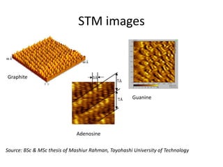
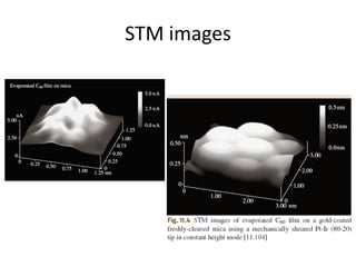
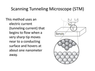
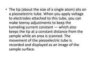
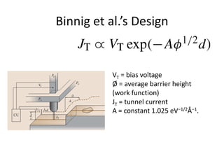
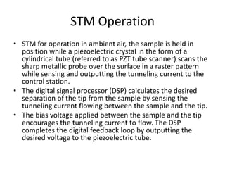
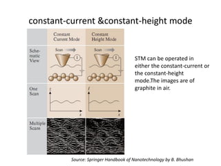
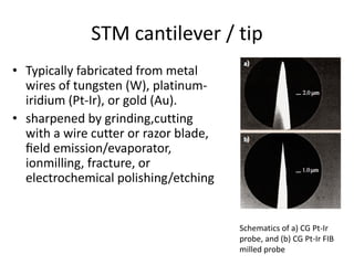
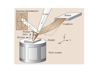
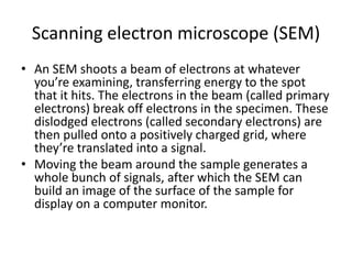
ETE444/544 :: Lecture 3

    Dr. Mashiur Rahman
AFM molecular recognition
        studies
Chemical Force Microscopy:
             General Methodology


Springer Handbook of Nanotechnology page 619
Adhesion at the Single-Bond Level


Springer Handbook of Nanotechnology page 622
Lecture 3

ETE444/544 Dr. Mashiur Rahman
Scanning Tunneling Microscope


-Springer Handbook of Nanotechnology Page 327 -
History
• The principle of electron tunneling was proposed by
  Giaever
   – I. Giaever: Energy gap in superconductors measured by
     electron tunneling, Phys. Rev. Lett. 5 (1960) 147–148
• He envisioned that if a potential difference is applied to
  two metals separated by a thin insulating film, a
  current will flow because of the ability of electrons to
  penetrate a potential barrier.
• To be able to measure a tunneling current, the two
  metals must be spaced no more than 10 nm apart.
Principle of STM
The principle of the STM is straightforward. A
  sharp metal tip (one electrode of the tunnel
  junction) is brought close enough (0.3–1 nm)
  to the surface to be investigated (the second
  electrode) that, at a convenient operating
  voltage (10 mV–1 V), the tunneling current
  varies from 0.2 to 10 nA which is measurable.
  The tip is scanned over a surface at a distance
  of 0.3–1 nm, while the tunneling current
  between it and the surface is measured.
Compact STM for use in controlled environments


2000, Toyohashi University of Technology, Japan
STM images


Graphite


                                                     Guanine


                              Adenosine

Source: BSc & MSc thesis of Mashiur Rahman, Toyohashi University of Technology
STM images
Scanning Tunneling Microscope (STM)

This method uses an
  electric current
  (tunneling current) that
  begins to flow when a
  very sharp tip moves
  near to a conducting
  surface and hovers at
  about one nanometer
  away.
• The tip (about the size of a single atom) sits on
  a piezoelectric tube. When you apply voltage
  to electrodes attached to this tube, you can
  make teensy adjustments to keep the
  tunneling current constant — which also
  keeps the tip at a constant distance from the
  sample while an area is scanned. The
  movement of the piezoelectric tube is
  recorded and displayed as an image of the
  sample surface.
Binnig et al.’s Design


           VT = bias voltage
           Ø = average barrier height
           (work function)
           JT = tunnel current
           A = constant 1.025 eV−1/2Å−1.
STM Operation
• STM for operation in ambient air, the sample is held in
  position while a piezoelectric crystal in the form of a
  cylindrical tube (referred to as PZT tube scanner) scans the
  sharp metallic probe over the surface in a raster pattern
  while sensing and outputting the tunneling current to the
  control station.
• The digital signal processor (DSP) calculates the desired
  separation of the tip from the sample by sensing the
  tunneling current flowing between the sample and the tip.
• The bias voltage applied between the sample and the tip
  encourages the tunneling current to flow. The DSP
  completes the digital feedback loop by outputting the
  desired voltage to the piezoelectric tube.
constant-current &constant-height mode


                                      STM can be operated in
                                      either the constant-current or
                                      the constant-height
                                      mode.The images are of
                                      graphite in air.


         Source: Springer Handbook of Nanotechnology by B. Bhushan
STM cantilever / tip
• Typically fabricated from metal
  wires of tungsten (W), platinum-
  iridium (Pt-Ir), or gold (Au).
• sharpened by grinding,cutting
  with a wire cutter or razor blade,
  field emission/evaporator,
  ionmilling, fracture, or
  electrochemical polishing/etching


                                       Schematics of a) CG Pt-Ir
                                       probe, and (b) CG Pt-Ir FIB
                                       milled probe
STM Tips
• The two most commonly used tips are
  – Pt-Ir (80/20) Iridium: tips are generally
    mechanically formed and are readily available.
    provide better atomic resolution than tungsten
    tips.
  – Tungsten wire: are etched from tungsten wire with
    an electrochemical process. Tungsten tips are
    more uniformly shaped and may perform better
    on samples with steeply sloped features.
Mechanically cut and electrochemically
                 etched STM tips


A mechanically cut STM tip (left) and an electrochemically etched STM tip (right),


p.383 Springer Handbook of Nanotechnology
Sample should be conductive
• Samples to be imaged with the STM must be
  conductive enough to allow a few
  nanoamperes of current to flow from the bias
  voltage source to the area to be scanned.
• In many cases, nonconductive samples can be
  coated with a thin layer of a conductive
  material to facilitate imaging.
• The bias voltage and the tunneling current
  depend on the sample.
piezoelectric tube
• If you put electrodes on the opposite sides of
  some crystals — quartz or topaz, for example —
  and apply a voltage across the crystal, it will
  expand or contract. Any movement of the crystal
  in response to a voltage is called the piezoelectric
  effect.
• The piezoelectric tube used in the scanning
  tunneling microscope is simply a crystal that
  expands or contracts depending upon the voltage
  you apply to it.
Scanning electron microscope (SEM)
• An SEM shoots a beam of electrons at whatever
  you’re examining, transferring energy to the spot
  that it hits. The electrons in the beam (called primary
  electrons) break off electrons in the specimen. These
  dislodged electrons (called secondary electrons) are
  then pulled onto a positively charged grid, where
  they’re translated into a signal.
• Moving the beam around the sample generates a
  whole bunch of signals, after which the SEM can
  build an image of the surface of the sample for
  display on a computer monitor.
Using SEM
SEMs can ferret out quite a bit of information about the
  sample:
• Topography: surface features such as texture
• Morphology: shape, size, and arrangements of the
  particles that compose the object’s surface
• Composition: elements that make up the sample
  (This can be determined by measuring the X-rays
  produced when the electron beam hits the sample.)
Transmission electron microscope (TEM)

• It’s a kind of nano-scale slide projector: Instead of shining a
  light through a photographic image the TEM sends a beam of
  electrons through a sample.
• The electrons that get through then strike a phosphor screen,
  producing a projected image: Darker areas indicate that fewer
  electrons got through; lighter areas are where more electrons
  got through
• A TEM can achieve a resolution of approximately 0.2
  nanometers, roughly the size of many atoms.
• A TEM can produce images that show you just how the atoms
  are arranged in a material.

ETE444-lec3.pdf

  • 1.
    ETE444/544 :: Lecture3 Dr. Mashiur Rahman
  • 2.
  • 3.
    Chemical Force Microscopy: General Methodology Springer Handbook of Nanotechnology page 619
  • 5.
    Adhesion at theSingle-Bond Level Springer Handbook of Nanotechnology page 622
  • 9.
  • 10.
    Scanning Tunneling Microscope -SpringerHandbook of Nanotechnology Page 327 -
  • 11.
    History • The principleof electron tunneling was proposed by Giaever – I. Giaever: Energy gap in superconductors measured by electron tunneling, Phys. Rev. Lett. 5 (1960) 147–148 • He envisioned that if a potential difference is applied to two metals separated by a thin insulating film, a current will flow because of the ability of electrons to penetrate a potential barrier. • To be able to measure a tunneling current, the two metals must be spaced no more than 10 nm apart.
  • 12.
    Principle of STM Theprinciple of the STM is straightforward. A sharp metal tip (one electrode of the tunnel junction) is brought close enough (0.3–1 nm) to the surface to be investigated (the second electrode) that, at a convenient operating voltage (10 mV–1 V), the tunneling current varies from 0.2 to 10 nA which is measurable. The tip is scanned over a surface at a distance of 0.3–1 nm, while the tunneling current between it and the surface is measured.
  • 13.
    Compact STM foruse in controlled environments 2000, Toyohashi University of Technology, Japan
  • 14.
    STM images Graphite Guanine Adenosine Source: BSc & MSc thesis of Mashiur Rahman, Toyohashi University of Technology
  • 15.
  • 16.
    Scanning Tunneling Microscope(STM) This method uses an electric current (tunneling current) that begins to flow when a very sharp tip moves near to a conducting surface and hovers at about one nanometer away.
  • 17.
    • The tip(about the size of a single atom) sits on a piezoelectric tube. When you apply voltage to electrodes attached to this tube, you can make teensy adjustments to keep the tunneling current constant — which also keeps the tip at a constant distance from the sample while an area is scanned. The movement of the piezoelectric tube is recorded and displayed as an image of the sample surface.
  • 18.
    Binnig et al.’sDesign VT = bias voltage Ø = average barrier height (work function) JT = tunnel current A = constant 1.025 eV−1/2Å−1.
  • 19.
    STM Operation • STMfor operation in ambient air, the sample is held in position while a piezoelectric crystal in the form of a cylindrical tube (referred to as PZT tube scanner) scans the sharp metallic probe over the surface in a raster pattern while sensing and outputting the tunneling current to the control station. • The digital signal processor (DSP) calculates the desired separation of the tip from the sample by sensing the tunneling current flowing between the sample and the tip. • The bias voltage applied between the sample and the tip encourages the tunneling current to flow. The DSP completes the digital feedback loop by outputting the desired voltage to the piezoelectric tube.
  • 20.
    constant-current &constant-height mode STM can be operated in either the constant-current or the constant-height mode.The images are of graphite in air. Source: Springer Handbook of Nanotechnology by B. Bhushan
  • 21.
    STM cantilever /tip • Typically fabricated from metal wires of tungsten (W), platinum- iridium (Pt-Ir), or gold (Au). • sharpened by grinding,cutting with a wire cutter or razor blade, field emission/evaporator, ionmilling, fracture, or electrochemical polishing/etching Schematics of a) CG Pt-Ir probe, and (b) CG Pt-Ir FIB milled probe
  • 22.
    STM Tips • Thetwo most commonly used tips are – Pt-Ir (80/20) Iridium: tips are generally mechanically formed and are readily available. provide better atomic resolution than tungsten tips. – Tungsten wire: are etched from tungsten wire with an electrochemical process. Tungsten tips are more uniformly shaped and may perform better on samples with steeply sloped features.
  • 23.
    Mechanically cut andelectrochemically etched STM tips A mechanically cut STM tip (left) and an electrochemically etched STM tip (right), p.383 Springer Handbook of Nanotechnology
  • 24.
    Sample should beconductive • Samples to be imaged with the STM must be conductive enough to allow a few nanoamperes of current to flow from the bias voltage source to the area to be scanned. • In many cases, nonconductive samples can be coated with a thin layer of a conductive material to facilitate imaging. • The bias voltage and the tunneling current depend on the sample.
  • 25.
    piezoelectric tube • Ifyou put electrodes on the opposite sides of some crystals — quartz or topaz, for example — and apply a voltage across the crystal, it will expand or contract. Any movement of the crystal in response to a voltage is called the piezoelectric effect. • The piezoelectric tube used in the scanning tunneling microscope is simply a crystal that expands or contracts depending upon the voltage you apply to it.
  • 27.
    Scanning electron microscope(SEM) • An SEM shoots a beam of electrons at whatever you’re examining, transferring energy to the spot that it hits. The electrons in the beam (called primary electrons) break off electrons in the specimen. These dislodged electrons (called secondary electrons) are then pulled onto a positively charged grid, where they’re translated into a signal. • Moving the beam around the sample generates a whole bunch of signals, after which the SEM can build an image of the surface of the sample for display on a computer monitor.
  • 28.
    Using SEM SEMs canferret out quite a bit of information about the sample: • Topography: surface features such as texture • Morphology: shape, size, and arrangements of the particles that compose the object’s surface • Composition: elements that make up the sample (This can be determined by measuring the X-rays produced when the electron beam hits the sample.)
  • 29.
    Transmission electron microscope(TEM) • It’s a kind of nano-scale slide projector: Instead of shining a light through a photographic image the TEM sends a beam of electrons through a sample. • The electrons that get through then strike a phosphor screen, producing a projected image: Darker areas indicate that fewer electrons got through; lighter areas are where more electrons got through • A TEM can achieve a resolution of approximately 0.2 nanometers, roughly the size of many atoms. • A TEM can produce images that show you just how the atoms are arranged in a material.