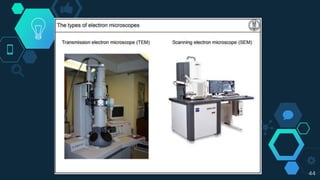
The document provides an overview of scanning electron microscopes (SEMs), including their history, key parts, working principle, applications, and sample preparation process. Some key points:
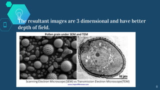
- SEMs use a beam of electrons to produce high-resolution images of sample surfaces, allowing examination of microscopic structural features. They have greater depth of field than light microscopes.
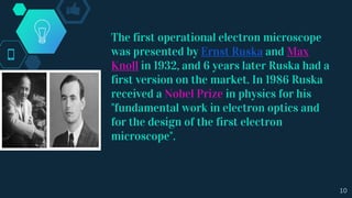
- Early development began in the 1930s. Commercial instruments became available in the 1960s. Continued improvements have increased resolution to the atomic scale.
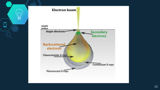
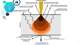
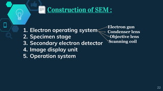
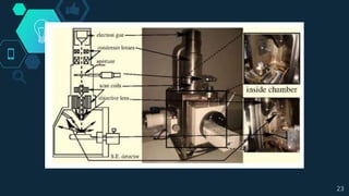
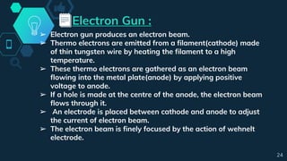
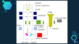
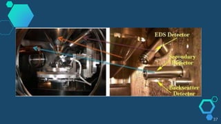
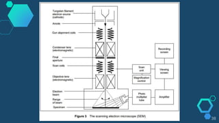
- Key components include an electron gun, electromagnetic lenses, vacuum system, specimen stage, and detectors. Secondary electrons emitted from the sample are used to form images.
- Applications span biology, materials
Today, scanning electron microscopy (SEM) is a versatile technique used in many
industrial labs, as well as for research and development. Due to its high lateral resolution, its great depth of focus and its facility for X-ray microanalysis, SEM is ofen
used in materials science – including polymer science – to elucidate the microscopic
structure or to differentiate several phases from each other.
Beam of electrons is transmitted through an ultra thin specimen,
An image is formed from the interaction of the electrons transmitted through the specimen,
The image is magnified and focused onto an imaging device, such as a fluorescent screen, on a layer of photographic film, or to be detected by a sensor such as a CCD camera
The transmission electron microscope is a very powerful tool for material science. A high energy beam of electrons is shone through a very thin sample, and the interactions between the electrons and the atoms can be used to observe features such as the crystal structure and features in the structure like dislocations and grain boundaries. Chemical analysis can also be performed. TEM can be used to study the growth of layers, their composition and defects in semiconductors. High resolution can be used to analyze the quality, shape, size and density of quantum wells, wires and dots.
Transmission electron microscopy (TEM) is a microscopy technique in which a beam of electrons is guided through an ultra thin specimen, interacting with the specimen as it passes through.An image is formed from the fundamental interaction of the electrons transmitted through the specimen; the image is magnified and focused onto an imaging device, such as a fluorescent screen, on a layer of photographic film, or to be observed by a sensor such as a CCD camera.
Electron microscope, principle and applicationKAUSHAL SAHU
Introduction
History
Resolution &Magnification of
Electron microscope
Types of electron microscope
1) Transmission electron microscope (TEM)
- Structural parts of TEM
- Principle & Working of TEM
- Sample preparation for TEM
- Advantages & disadvantages of TEM
Scanning electron microscope (SEM)
- Structural parts of SEM
- Principle & Working of SEM
- Sample preparation for SEM
- Advantages & disadvantages of SEM
3) Scanning transmission electron microscope (STEM)
Applications of electron microscope
Conclusion
References
Electron Microscopy - Scanning electron microscope, Transmission Electron Mic...Sumer Pankaj
An electron microscope is a microscope that uses a beam of accelerated electrons as a source of illumination. As the wavelength of an electron can be up to 100,000 times shorter than that of visible light photons, electron microscopes have a higher resolving power than light microscopes and can reveal the structure of smaller objects. A transmission electron microscope can achieve better than 50 pm resolution and magnifications of up to about 10,000,000x whereas most light microscopes are limited by diffraction to about 200 nm resolution and useful magnifications below 2000x.
Electron microscopes are used to investigate the ultrastructure of a wide range of biological and inorganic specimens including microorganisms, cells, large molecules, biopsy samples, metals, and crystals. Industrially, electron microscopes are often used for quality control and failure analysis. Modern electron microscopes produce electron micrographs using specialized digital cameras and frame grabbers to capture the image.
A scanning electron microscope (SEM) is a type of electron microscope that produces images of a sample by scanning the surface with a focused beam of electrons.
5. Microsocope ELECTRON MICROSCOPE (TEM & SEM ) - BasicsNethravathi Siri
Basics only
Electron beam is the source of illumination.
Image is produced by magnetic field.
Contrasting features between light microscope and electron microscope are
construction, working principle, specimen preparation, cost-expenses and designed
room (vacuum chamber).
Scanning electron micronscope - Its applicability in the field of ayurveda (Rassashastra) to find find out the size of the bhasma particle its distribution and view 3D crystalline structure view of bhasmas. The resoluton in scanning electron microscope is greater hence views better images of bhasmas. SEM is most commonly used in the field of rasashastra. SEM analysis very much useful in nanomedicine for viewing the particle sizes in greater resolutions. SEM analysis is a step in standisation of ayurvedic bhasmas. Apart ffrom bhasma pariksha vidhis in ayurveda this novel instrument applicability on in the field of rasashastra helps to find the exact size of the particle.
Unit 8 - Information and Communication Technology (Paper I).pdfThiyagu K
This slides describes the basic concepts of ICT, basics of Email, Emerging Technology and Digital Initiatives in Education. This presentations aligns with the UGC Paper I syllabus.
Honest Reviews of Tim Han LMA Course Program.pptxtimhan337
Personal development courses are widely available today, with each one promising life-changing outcomes. Tim Han’s Life Mastery Achievers (LMA) Course has drawn a lot of interest. In addition to offering my frank assessment of Success Insider’s LMA Course, this piece examines the course’s effects via a variety of Tim Han LMA course reviews and Success Insider comments.
Palestine last event orientationfvgnh .pptxRaedMohamed3
An EFL lesson about the current events in Palestine. It is intended to be for intermediate students who wish to increase their listening skills through a short lesson in power point.
Francesca Gottschalk - How can education support child empowerment.pptxEduSkills OECD
Francesca Gottschalk from the OECD’s Centre for Educational Research and Innovation presents at the Ask an Expert Webinar: How can education support child empowerment?
Biological screening of herbal drugs: Introduction and Need for
Phyto-Pharmacological Screening, New Strategies for evaluating
Natural Products, In vitro evaluation techniques for Antioxidants, Antimicrobial and Anticancer drugs. In vivo evaluation techniques
for Anti-inflammatory, Antiulcer, Anticancer, Wound healing, Antidiabetic, Hepatoprotective, Cardio protective, Diuretics and
Antifertility, Toxicity studies as per OECD guidelines
June 3, 2024 Anti-Semitism Letter Sent to MIT President Kornbluth and MIT Cor...Levi Shapiro
Letter from the Congress of the United States regarding Anti-Semitism sent June 3rd to MIT President Sally Kornbluth, MIT Corp Chair, Mark Gorenberg
Dear Dr. Kornbluth and Mr. Gorenberg,
The US House of Representatives is deeply concerned by ongoing and pervasive acts of antisemitic
harassment and intimidation at the Massachusetts Institute of Technology (MIT). Failing to act decisively to ensure a safe learning environment for all students would be a grave dereliction of your responsibilities as President of MIT and Chair of the MIT Corporation.
This Congress will not stand idly by and allow an environment hostile to Jewish students to persist. The House believes that your institution is in violation of Title VI of the Civil Rights Act, and the inability or
unwillingness to rectify this violation through action requires accountability.
Postsecondary education is a unique opportunity for students to learn and have their ideas and beliefs challenged. However, universities receiving hundreds of millions of federal funds annually have denied
students that opportunity and have been hijacked to become venues for the promotion of terrorism, antisemitic harassment and intimidation, unlawful encampments, and in some cases, assaults and riots.
The House of Representatives will not countenance the use of federal funds to indoctrinate students into hateful, antisemitic, anti-American supporters of terrorism. Investigations into campus antisemitism by the Committee on Education and the Workforce and the Committee on Ways and Means have been expanded into a Congress-wide probe across all relevant jurisdictions to address this national crisis. The undersigned Committees will conduct oversight into the use of federal funds at MIT and its learning environment under authorities granted to each Committee.
• The Committee on Education and the Workforce has been investigating your institution since December 7, 2023. The Committee has broad jurisdiction over postsecondary education, including its compliance with Title VI of the Civil Rights Act, campus safety concerns over disruptions to the learning environment, and the awarding of federal student aid under the Higher Education Act.
• The Committee on Oversight and Accountability is investigating the sources of funding and other support flowing to groups espousing pro-Hamas propaganda and engaged in antisemitic harassment and intimidation of students. The Committee on Oversight and Accountability is the principal oversight committee of the US House of Representatives and has broad authority to investigate “any matter” at “any time” under House Rule X.
• The Committee on Ways and Means has been investigating several universities since November 15, 2023, when the Committee held a hearing entitled From Ivory Towers to Dark Corners: Investigating the Nexus Between Antisemitism, Tax-Exempt Universities, and Terror Financing. The Committee followed the hearing with letters to those institutions on January 10, 202
Welcome to TechSoup New Member Orientation and Q&A (May 2024).pdfTechSoup
In this webinar you will learn how your organization can access TechSoup's wide variety of product discount and donation programs. From hardware to software, we'll give you a tour of the tools available to help your nonprofit with productivity, collaboration, financial management, donor tracking, security, and more.
How to Make a Field invisible in Odoo 17Celine George
It is possible to hide or invisible some fields in odoo. Commonly using “invisible” attribute in the field definition to invisible the fields. This slide will show how to make a field invisible in odoo 17.
The Roman Empire A Historical Colossus.pdfkaushalkr1407
The Roman Empire, a vast and enduring power, stands as one of history's most remarkable civilizations, leaving an indelible imprint on the world. It emerged from the Roman Republic, transitioning into an imperial powerhouse under the leadership of Augustus Caesar in 27 BCE. This transformation marked the beginning of an era defined by unprecedented territorial expansion, architectural marvels, and profound cultural influence.
The empire's roots lie in the city of Rome, founded, according to legend, by Romulus in 753 BCE. Over centuries, Rome evolved from a small settlement to a formidable republic, characterized by a complex political system with elected officials and checks on power. However, internal strife, class conflicts, and military ambitions paved the way for the end of the Republic. Julius Caesar’s dictatorship and subsequent assassination in 44 BCE created a power vacuum, leading to a civil war. Octavian, later Augustus, emerged victorious, heralding the Roman Empire’s birth.
Under Augustus, the empire experienced the Pax Romana, a 200-year period of relative peace and stability. Augustus reformed the military, established efficient administrative systems, and initiated grand construction projects. The empire's borders expanded, encompassing territories from Britain to Egypt and from Spain to the Euphrates. Roman legions, renowned for their discipline and engineering prowess, secured and maintained these vast territories, building roads, fortifications, and cities that facilitated control and integration.
The Roman Empire’s society was hierarchical, with a rigid class system. At the top were the patricians, wealthy elites who held significant political power. Below them were the plebeians, free citizens with limited political influence, and the vast numbers of slaves who formed the backbone of the economy. The family unit was central, governed by the paterfamilias, the male head who held absolute authority.
Culturally, the Romans were eclectic, absorbing and adapting elements from the civilizations they encountered, particularly the Greeks. Roman art, literature, and philosophy reflected this synthesis, creating a rich cultural tapestry. Latin, the Roman language, became the lingua franca of the Western world, influencing numerous modern languages.
Roman architecture and engineering achievements were monumental. They perfected the arch, vault, and dome, constructing enduring structures like the Colosseum, Pantheon, and aqueducts. These engineering marvels not only showcased Roman ingenuity but also served practical purposes, from public entertainment to water supply.
Macroeconomics- Movie Location
This will be used as part of your Personal Professional Portfolio once graded.
Objective:
Prepare a presentation or a paper using research, basic comparative analysis, data organization and application of economic information. You will make an informed assessment of an economic climate outside of the United States to accomplish an entertainment industry objective.
4. Introduction :
The scanning electron microscope is one of the most
versatile instruments available for examination and analysis
of the microstructural characteristics of solid objects.
The primary reason for the SEMs usefulness is the high
resolution which can be obtained when bulk objects are
examined.
Another important feature of SEM images is the three
dimensional appearance of specimen, which is a result of
large depth of focus. 4
5. ➔ SEM can provide useful information about the
composition at the specimen surface.
➔ The user can obtain high magnification images, with
a good depth of field, and can also analyse individual
crystals or other features.
➔ A high-resolution SEM image can show detail down
to 25 Angstroms, or better.
➔ When used in conjunction with the closely-related
technique of energy-dispersive X-ray microanalysis
(EDX, EDS, EDAX), the composition of individual
crystals or features can be determined.
5
7. ➔ The area to be examined is irradiated with a finely
focused beam of electrons which may be static or
swept in a raster across the surface of the specimen.
➔ They are obtained from specific emission volumes
within the sample and are used to measure many
characteristics of the sample (composition, surface
topography , crystallography,)
7
10. The first operational electron microscope
was presented by Ernst Ruska and Max
Knoll in 1932, and 6 years later Ruska had a
first version on the market. In 1986 Ruska
received a Nobel Prize in physics for his
"fundamental work in electron optics and
for the design of the first electron
microscope".
10
11. The invention of the electron microscope by Max
Knoll and Ernst Ruska at the Berlin Technische
Hochschule in 1931 finally overcame the barrier to
higher resolution that had been imposed by the
limitations of visible light. Since then resolution
has defined the progress of the technology. The
ultimate goal was atomic resolution - the ability to
see atoms. To avoid the effects of objective lens
chromatic aberration with thick samples in TEM
, SEM was invented.
11
12. It was Manfred von Ardenne in 1937 invented
SEM. Further work was reported by Zworykin's
group, followed by the Cambridge groups in the
1950s and early 1960s headed by Charles Oatley,
all of which finally led to the marketing of the
first commercial instrument by Cambridge
Scientific Instrument Company as the
"Stereoscan" in 1965, which was delivered to
DuPont.
12
13. Applications of SEM:
Scanning Electron Microscopy - SEM - is a
powerful technique in the examination of
materials. It is used widely in metallurgy,
geology, biology and medicine, to name just a few.
13
15. BIOMEDICAL ENGINEERING
SEMs combine the latest concepts from medicine,
biotechnology and engineering for designing a
variety of technologies such as support matrices for
cell growth, artificial tissue and implantable
biomedical device.
Growth of osteoblasts on
zirconia ceramics
15
16. CELL & TISSUE MORPHOLOGY
SEMs are the ideal instruments for investigating cellular and
tissue structure with high resolution. Typical applications involve
observing shape changes of grooves, pores, blebs or microvilli on
the cellular in response to the changes in the extracellular
environment.
Detail of a fibroblast cell
16
17. MICROBIOLOGY
High resolution imaging of the microbial surface using SEM
helps to have a better understanding of the morphology of
microbial populations, bacteria communication and biofilm
formation. SEMs help researchers visualize microbial
populations with great focal depth and high resolution.
S.mutans on dental
filling
17
18. SUBCELLULAR ANALYSIS
The SEM technology is becoming more popular in this field, due to
emerging techniques which are available to scanning electron
microscopy. SEM offers several solutions for scientists interested in
the subcellular investigations of biological samples.
Osteoblast layer in a
mouse tooth.
18
19. Principle
In a scanning electron microscope, the specimen
is exposed to a narrow electron beam from an electron
gun, which rapidly moves over or scans the surface of the
specimen.
This causes the release of a shower of secondary electrons
and other types of radiations from the specimen surface.
The intensity of these secondary electrons depends upon
the shape and the chemical composition of the irradiated
object. These electrons are collected by a detector, which
generates electronic signals.
19
22. Construction of SEM :
1. Electron operating system
2. Specimen stage
3. Secondary electron detector
4. Image display unit
5. Operation system
Electron gun
Condenser lens
Objective lens
Scanning coil
22
24. Electron Gun :
➢ Electron gun produces an electron beam.
➢ Thermo electrons are emitted from a filament(cathode) made
of thin tungsten wire by heating the filament to a high
temperature.
➢ These thermo electrons are gathered as an electron beam
flowing into the metal plate(anode) by applying positive
voltage to anode.
➢ If a hole is made at the centre of the anode, the electron beam
flows through it.
➢ An electrode is placed between cathode and anode to adjust
the current of electron beam.
➢ The electron beam is finely focused by the action of wehnelt
electrode.
24
26. Construction of lens :
➢ A direct electric current is passed through
a coil wound electric wire a rotationally
symmetric magnetic field is formed and a lens
action is produced on electron beam.
➢ The surrounding of the coil is enclosed by
yoke so that part of magnetic field leaks out
from a narrow gap.
➢ A portion with narrow gap is called pole
piece.
➢ When the current passing through the coil changes, the strength
of coil is also changed which is not possible in light microscope.
26
28. Condenser lens and objective lens
● Two stage lenses which combine the condenser and objective
lenses are located below the electron gun.
● The electron beam from the electron gun is focused by the 2 stage
lenses and a small electron probe is produced.
● Placing a lens below the electron gun enables you to adjust the
diameter of electron beam.
● A fine electron beam is required for SEM.
● The aperture is placed between condenser and objective lens.
● The aperture is made of thin metal plate and has a small hole.
28
30. ● The electron beam, which passed through the
condenser lens illuminates this aperture plate.
● The aperture allows a part of electron beam to
reach the objective lens.
● The objective lens is used for focusing.
● It determines the final diameter of electron
probe.
● If the objective lens is not good, an optimally
fine electron probe cannot be produced .
30
31. Specimen stage
➔ In general, the specimen is observed at higher
magnification in an electron microscope.
➔ Thus a specimen stage which stably supports the
specimen and moves smoothly is required.
➔ The specimen stage in SEM can perform following
movements:
- Horizontal movement
- Vertical movement
- Specimen tilting
- Rotation
Change of image resolution
Selection of field of view
31
33. ● Most SEMs use eucentric specimen
stage.
● By the use of this stage the specimen
does not change after shifting the
field of view when the specimen is
tilted.
● In addition to manual drive stage, the
use of motor driven stage has
increased.
● In computer controlled specimen
stage, the stage can be moved to
selected point by simply clicking
mouse and restore the stage to
desired observed point.
33
34. Secondary electron detector
➔ The secondary electron detector detects secondary electrons emitted
from specimen invented by Everhart and Thornley. Also called E-T
detector.
➔ A scintillator (fluorescent) substance is coated on the tip of the
detector and a high voltage of 10kv is applied to it.
➔ The secondary electrons from the specimen are attracted to this high
voltage and then generate light when they hit the scintillator.
➔ This light is directed to a photomultiplier tube (PMT) through a light
guide.
➔ Then the light is converted to electrons and these electrons are
amplified as an electric signal.
➔ This is present in sample chamber nearer to objective lens.
34
39. Preparation of sample
➔ Treatment of biological specimens involves
following procedure:
- Removing and cleaning of tissues
- Fixation
- Dehydration
- Drying
- Mounting and coating
Coating is same as for other non conductive
specimens. It is coated with a thin metal film so that
surface has conductivity.
39
40. 40
Coating
➔ The dried specimen is mounted on an aluminium stub.
➔ A simple adhesive like durofix may be used.
➔ The specimen is placed in the chamber of a sputter
coating unit and air is evacuated by purging the
chamber with argon for 2 mins.
➔ When vacuum of 0.1torr is attained gold is discharged
from a target situated above the specimen and
deposited on the surface of sample.
➔ The thickness of the layer of gold is determined by the
distance of the specimen from the target, period of time
taken to sputter and strength of current applied to
target.
41. 41
Cryopreservation:
➔ Eliminates the artefacts associated with fixation,
dehydration and embedding.
➔ There are now cryosystems which interface directly to
SEM which allow fresh tissue to be frozen rapidly with
liquid nitrogen, sputtered with gold and then examined in
SEM while it is still frozen.
➔ These cryosystems consists of
- Slushing chamber to freeze specimen
- Low temperature preparation chamber in which
specimens may be fractured have the ice sublimed from
their surface and be coated. This preparation chamber
can be fitted directly to SEM or may be a separate unit.
42. Differences between TEM and SEM
SEM TEM
Scattered electrons Transmitted electrons
Larger samples can be examined. Sample has to be cut into thinner
sections.
Large amount of sample can be
examined at a time.
Only small amount of sample can
be examined at a time.
Comparatively lesser resolution. Resolution is greater than SEM.
Effective Instrument Resolution -
1nm
Effective Instrument Resolution -
0.5nm 42
53. 53
References :
● Cullings handbook of histopathological and histochemical techniques - 3rd
edition.
● Bancroft book of histopathology - 7th edition.
● Various internet sources