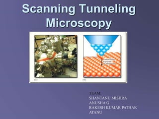
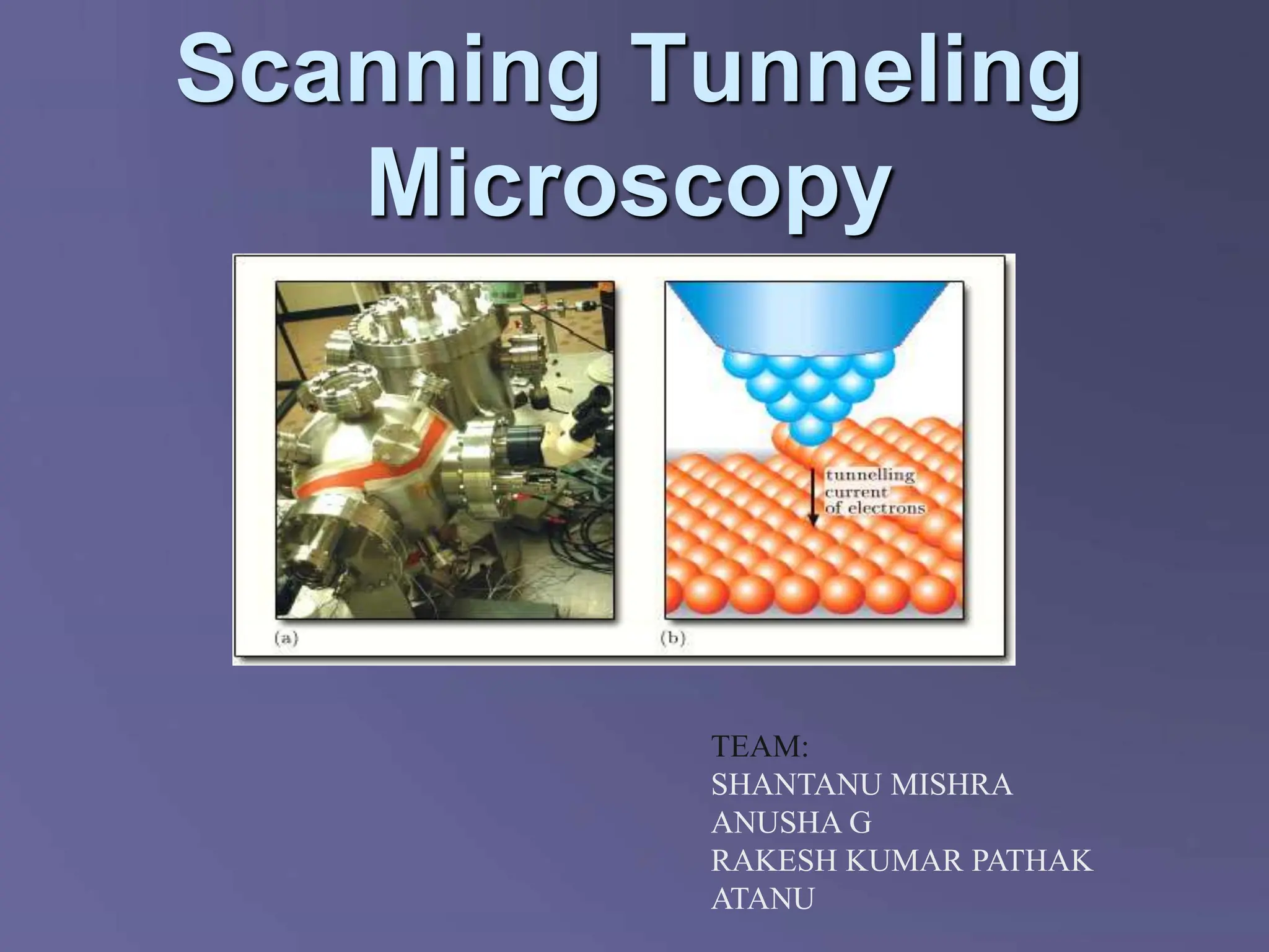
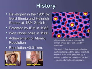
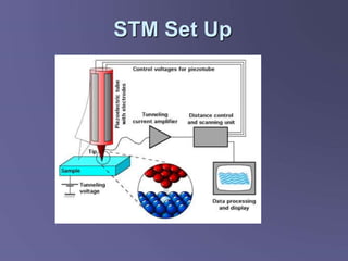
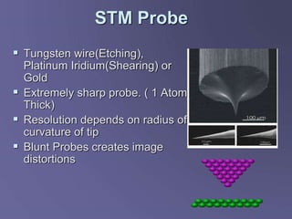
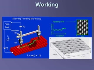
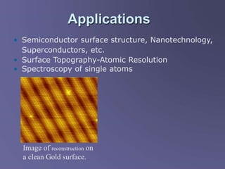
Scanning Tunneling
Microscopy
TEAM:
SHANTANU MISHRA
ANUSHA G
RAKESH KUMAR PATHAK
ATANU
Contents
 History
 Introduction
 Some Definitions
 Basic Principle
 Set-Up
 Applications
History
 Developed in the 1981 by
Gerd Binnig and Heinrich
Rohrer at IBM Zürich .
 Patented by IBM in 1982.
 Won Nobel prize in 1986.
 Achievement of Atomic
Resolution
 Resolution:~0.01 nm.
silicon surface atoms enlarged 20
million times, color-enhanced by
computer.
The world's first images of individual
surface atoms and the bonds that hold
them in place were produced by a
research technique developed by IBM -
- scanning tunneling microscopy.
Introduction
 Scanning tunneling microscope (STM) is a powerful technique for viewing
surfaces at the atomic level.
 STM probes the density of states of a material using tunneling current.
 The STM is based on the concept of Quantum Tunneling.
General Overview
1. An extremely fine conducting probe is held
about an atom’s diameter from the sample.
2. Electrons tunnel between the surface and the tip,
producing an electrical signal.
3. While it slowly scans across the surface,
the tip is raised and lowered in order to keep
the signal constant and maintain the distance.
This enables it to follow even the smallest
details of the surface it is scanning.
Note
A STM does not measure nuclear position
directly. Rather it measures the electron
density clouds on the surface of the sample.
In some cases, the electron clouds represent
the atom locations pretty well, but not
always.
Quantum Tunneling
Classically, when an object hits a potential that
it doesn’t have enough energy to pass, it will
never go though that potential wall, it always
bounces back.
In English, if you throw a ball at a wall, it will
bounce back at you.
Classical
Wave Function
For Finite Square
Well Potential
Where E<V
Quantum Tunneling
In quantum mechanics when a particle hits a
potential that it doesn’t have enough energy
to pass, when inside the square well, the wave
function dies off exponentially.
If the well is short enough, there will be a noticeable
probability of finding the particle on the other side.
Quantum
Wave Function
For Finite Square
Well Potential
Where E<V
Quantum Tunneling
The finite square well potential is a good
approximation for looking at electrons on conducting
slabs with a gap between them.
So what is this tunneling in STM?
 When a conducting tip is brought very near to a metallic
or semi- conducting surface, a bias between the two can
allow electrons to tunnel through the vacuum between
them.
 In order to understand this tunneling effect, next we have
to talk about "density of states".
Density of States
The electrons fill up the energy valley in the sample until there are no more
electrons. The top energy level at which electrons sit is called the Fermi level,
eF. For every energy e, the density of states is the number of electrons sitting
within De of e, divided by De.
Electrons in an isolated atom live at specific discrete energy levels. In case of
metal the levels are so close together that instead to list the energy levels of all
the electrons we say energy interval De around energy e.
Vaccum Barrier
 The electrons in the tip and the sample are sitting in two separate valleys,
separated by a hill which is the vacuum barrier.
Tunneling of Electron
By applying a bias voltage to the sample with respect to
the tip, we effectively raise the Fermi level of the
sample with respect to the tip. Now we have empty
states available for tunneling into.
Quantum Tunneling
More graphs of tunneling:
An electron tunneling from atom to atom:
n(r) is the
probability of
finding an electron
V(r) is the potential
Quantum Tunneling
Now looking more in depth at the case of tunneling
from one metal to another. EF represents the Fermi
energy. Creating a voltage drop between the two
metals allows current.
Tip
Sample
Quantum Tunneling
Through a barrier, quantum mechanics predicts that the
wave function dies off exponentially:
So the probability of finding an electron after a barrier of
width d is:
And:
Where f(V) is the Fermi function, which contains a weighted
joint local density of states. This a material property obtained
by measurements.
Quantum Tunneling
Plugging in typical values for m, d, and phi (where
phi is the average work function of the tip and the
sample), when d changes by 1 Å, the current
changes by a factor of about 10!
Where:
Quantum Tunneling
So if you bring the tip close enough to the surface,
you can create a tunneling current,
even though there is a break in the circuit.
The size of the gap in practice is on the order
of a couple of Angstroms (10-10 m)!
As you can see, the current is VERY sensitive to the
gap distance.
Basics of STM
 Tunnelling current as a measure of surface characteristics
 Sharp probe & prepared surface of sample
 Bringing them close(4-7 A°) & Bias Voltage(1V) results in
Tunnelling (I=O(nA))
 Used in UHV
 Current is very sensitive to the gap between the tip and
the surface
d ~ 6
Å
Bias voltage:
mV – V range
Why such a fine tip is required?
The second tip shown above is recessed by about two atoms
and thus carries about a million times less current. That is
why we want such a fine tip. If we can get a single atom at
the tip, the vast majority of the current will run through it
and thus give us atomic resolution.
STM Set Up
Instrumentation
 Piezoelectric Transducer used for controlled
movement in XYZ (+/- .05A°)
 Coarse positioner
 Mechanism for vibration isolation (Coil springs
& Magnetic Damper)
 Noise Cancellation Final image enhanced
through image processing
 Feedback control used for height adjustment
STM Probe
 Tungsten wire(Etching),
Platinum Iridium(Shearing) or
Gold
 Extremely sharp probe. ( 1 Atom
Thick)
 Resolution depends on radius of
curvature of tip
 Blunt Probes creates image
distortions
STM tip: atomically sharp needle and terminates in a single atom
Pure metals (W, Au)
Alloys (Pt-Rh, Pt-Ir)
Chemically modified conductor (W/S, Pt-Rh/S, W/C…)
Preparation of tips: Cut by a wire cutter and used as is cut
followed by electrochemical etching
Small Movements
To get the distance between the tip and the
sample down to a couple of Angstroms
where the tunneling current is at a measurable
level, STMs use feedback servo loops and converse
piezoelectricity.
Servos
Servos are small devices with a shaft that
can be precisely controlled with electrical
signals.
Servos are used all the time in radio
controlled cars, puppets, and robots.
Converse Piezoelectricity
Piezoelectricity is the ability of certain crystals to
produce a voltage when subjected to mechanical
stress.
When you apply an electric field to a piezoelectric
crystal, the crystal distorts. This is known as
converse piezoelectricity. The distortions of a
piezo is usually on the order of micrometers,
which is in the scale needed to keep the tip of the
STM a couple Angstroms from the surface.
The tip
Pizos
Electric Field
Vibration-Isolation
The original STM design had the tunnel unit with
permanent magnets levitated on a superconducting lead
bowl. They used 20 L of liquid helium per hour.
Vibration-Isolation
The simple and presently widely used vibration protection
with a stack of metal plates separated by viton - an ultra
high vacuum compatible rubber spacer.
Problems and Solutions
• Bringing the tip close to the surface and scanning the surface
• Feedback Servo Loops
• Keeping the tip close to the surface
• Converse Piezoelectricity
• Creating a very fine tip
• Electro-chemical etching
• Forces between tip and sample
• Negligible in most cases
• Mechanical vibrations and acoustic noise
• Soft suspension of the microscope within an ultra high
vacuum chamber (10-11 Torr)
• Thermal length fluctuations of the sample and especially the tip
• Very low temperatures
• The sample has to be able to
conduct electricity
Working
Modes of Operation
Constant Height
• Variation of Current with lateral
distance
• Surface of density of state
• Faster Scanning Rate
Constant Current
• Feedback adjusts the height to
make current const
• Surfaces of const density of state
Image Interpretation
 Gives the density of state of
surfaces
 DOS- Number of electronic states
per unit volume per unit energy.
 For a large scale image –
Topography
Hydrogen on Gadolinium
Advantages
 Need for Vacuum & Vibration isolation
 Samples limited to conductors and semiconductors
 High Equipment cost
 Surface Preparation
 Maintaining the tool sharpness
Disadvantages
• High Resolution Images (Atomic scale).
• Low power application.
• No damage to the sample.
Applications
• Semiconductor surface structure, Nanotechnology,
Superconductors, etc.
• Surface Topography-Atomic Resolution
• Spectroscopy of single atoms
Image of reconstruction on
a clean Gold surface.
Typical Applications of STM
 Powerful imaging tool, directly visualize electrochemical
processes in-situ and in real space at molecular or
atomic levels.
 Such interfacial electrochemical studies have been
dramatically expanded over the past decade, covering
areas in electrode surfaces, metal deposition, charge
transfer, potential-dependent surface morphology,
corrosion, batteries, semiconductors, and
nanofabrication.
 Events in the EC data correlate with changes in the
topography of the sample surface.
Electrochemical STM (ECSTM)
Metal deposition
When applying an potential negative of the equilibrium potential Er to
cathode, bulk deposition of metal takes place.
As a nucleation-and-growth process, deposition of metal preferentially
occurs at the surface defects, such as steps or screw dislocations.
STM images of Au(111) surface in 5 mM H2SO4
+ 0.05 mM CuSO4 before (panel a) and
during (panel b) copper deposition.
The bare gold surface has atomically flat
terraces separated by three monoatomic
high steps.
After a potential step to negative values,
deposition of bulk Cu occurs almost
preferentially at the monoatomic high
steps, namely, the growing Cu clusters are
decorating the gold surface defects.
STM-based electrochemical nanotechnology
• STM tip: a tool for manipulating individual atoms or molecules on substrate
surface and directing them continuously to predetermined positions
• ECSTM tip-generated entities are clearly larger than single atoms due to their low
stability to survive electrochemical environment at room temperature.
• Tip crash method: (surface damaged ) use the tip to create surface defects, which
then acted as nucleation centers for the metal deposition at pre-selected positions.
• Jump-to-contact method: (surface undamaged ) metal is first deposited onto the tip
from electrolyte, then the metal-loaded tip approaches the surface to form a
connective neck between tip and substrate. Upon retreat of the tip and applying a
pulsed voltage, the neck breaks, leaving a metal cluster on the substrate. Continued
metal deposition onto the tip supplies enough material for the next cluster
generation.
Thank You
Question:
 At low voltages and temperature the tunneling current is given by:
 where d is the distance between the tip and sample, K is the decay
constant, m is the mass of an electron,  is the barrier height and
ħ is planks constant. Assume the local barrier height is about 4eV.
Show the current sensitivity to distance between the tip and
sample if the current is kept within 2%.





m
K
Kd
I
2
)
2
exp(
Answer
For
where
if current is kept to 2%,  = 4eV, then
Very sensitive technique!
 Another relevant question is, why do the electrons all sit
on top of each other, filling up the valley to energy eF?
Why wouldn't they all just clump together at the lowest
point at the bottom of the valley?
 The answer is that electrons are rather unfriendly characters called
fermions. No two fermions are allowed to occupy the same energy
state; this is known as the Pauli exclusion principle. So the
electrons must pile on top of each other instead.
References
G. Binnig and H. Rohrer. "Scanning Tunneling Microscopy", IBM J Res.
Develop., 30:355, 1986.
G. Binnig, H. Rohrer, “Scanning Tunneling Microscopy - From Birth to
Adolescence”, Nobel lecture, December 8, 1986.
Tit-Wah Hui, “Scanning Tunneling Microscopy - A Tutorial”,
http://www.chembio.uoguelph.ca/educmat/chm729/STMpage/stmtutor.htm
Wikipedia, “Scanning Tunneling Microscope”,
http://en.wikipedia.org/wiki/Scanning_tunneling_microscope
Nobel e-Museum, “The Scanning Tunneling Microscope”,
http://www.nobel.se/physics/educational/microscopes/scanning/index.html
Pictures from http://www.almaden.ibm.com/vis/stm/blue.html

STM finalfor scanningtunnelingmicroscope experiments.ppt

  • 1.
  • 2.
    Contents  History  Introduction Some Definitions  Basic Principle  Set-Up  Applications
  • 3.
    History  Developed inthe 1981 by Gerd Binnig and Heinrich Rohrer at IBM Zürich .  Patented by IBM in 1982.  Won Nobel prize in 1986.  Achievement of Atomic Resolution  Resolution:~0.01 nm. silicon surface atoms enlarged 20 million times, color-enhanced by computer. The world's first images of individual surface atoms and the bonds that hold them in place were produced by a research technique developed by IBM - - scanning tunneling microscopy.
  • 4.
    Introduction  Scanning tunnelingmicroscope (STM) is a powerful technique for viewing surfaces at the atomic level.  STM probes the density of states of a material using tunneling current.  The STM is based on the concept of Quantum Tunneling.
  • 5.
    General Overview 1. Anextremely fine conducting probe is held about an atom’s diameter from the sample. 2. Electrons tunnel between the surface and the tip, producing an electrical signal. 3. While it slowly scans across the surface, the tip is raised and lowered in order to keep the signal constant and maintain the distance. This enables it to follow even the smallest details of the surface it is scanning.
  • 6.
    Note A STM doesnot measure nuclear position directly. Rather it measures the electron density clouds on the surface of the sample. In some cases, the electron clouds represent the atom locations pretty well, but not always.
  • 7.
    Quantum Tunneling Classically, whenan object hits a potential that it doesn’t have enough energy to pass, it will never go though that potential wall, it always bounces back. In English, if you throw a ball at a wall, it will bounce back at you. Classical Wave Function For Finite Square Well Potential Where E<V
  • 8.
    Quantum Tunneling In quantummechanics when a particle hits a potential that it doesn’t have enough energy to pass, when inside the square well, the wave function dies off exponentially. If the well is short enough, there will be a noticeable probability of finding the particle on the other side. Quantum Wave Function For Finite Square Well Potential Where E<V
  • 9.
    Quantum Tunneling The finitesquare well potential is a good approximation for looking at electrons on conducting slabs with a gap between them.
  • 10.
    So what isthis tunneling in STM?  When a conducting tip is brought very near to a metallic or semi- conducting surface, a bias between the two can allow electrons to tunnel through the vacuum between them.  In order to understand this tunneling effect, next we have to talk about "density of states".
  • 11.
    Density of States Theelectrons fill up the energy valley in the sample until there are no more electrons. The top energy level at which electrons sit is called the Fermi level, eF. For every energy e, the density of states is the number of electrons sitting within De of e, divided by De. Electrons in an isolated atom live at specific discrete energy levels. In case of metal the levels are so close together that instead to list the energy levels of all the electrons we say energy interval De around energy e.
  • 12.
    Vaccum Barrier  Theelectrons in the tip and the sample are sitting in two separate valleys, separated by a hill which is the vacuum barrier.
  • 13.
    Tunneling of Electron Byapplying a bias voltage to the sample with respect to the tip, we effectively raise the Fermi level of the sample with respect to the tip. Now we have empty states available for tunneling into.
  • 14.
    Quantum Tunneling More graphsof tunneling: An electron tunneling from atom to atom: n(r) is the probability of finding an electron V(r) is the potential
  • 15.
    Quantum Tunneling Now lookingmore in depth at the case of tunneling from one metal to another. EF represents the Fermi energy. Creating a voltage drop between the two metals allows current. Tip Sample
  • 16.
    Quantum Tunneling Through abarrier, quantum mechanics predicts that the wave function dies off exponentially: So the probability of finding an electron after a barrier of width d is: And: Where f(V) is the Fermi function, which contains a weighted joint local density of states. This a material property obtained by measurements.
  • 17.
    Quantum Tunneling Plugging intypical values for m, d, and phi (where phi is the average work function of the tip and the sample), when d changes by 1 Å, the current changes by a factor of about 10! Where:
  • 18.
    Quantum Tunneling So ifyou bring the tip close enough to the surface, you can create a tunneling current, even though there is a break in the circuit. The size of the gap in practice is on the order of a couple of Angstroms (10-10 m)! As you can see, the current is VERY sensitive to the gap distance.
  • 19.
    Basics of STM Tunnelling current as a measure of surface characteristics  Sharp probe & prepared surface of sample  Bringing them close(4-7 A°) & Bias Voltage(1V) results in Tunnelling (I=O(nA))  Used in UHV  Current is very sensitive to the gap between the tip and the surface d ~ 6 Å Bias voltage: mV – V range
  • 20.
    Why such afine tip is required? The second tip shown above is recessed by about two atoms and thus carries about a million times less current. That is why we want such a fine tip. If we can get a single atom at the tip, the vast majority of the current will run through it and thus give us atomic resolution.
  • 21.
  • 22.
    Instrumentation  Piezoelectric Transducerused for controlled movement in XYZ (+/- .05A°)  Coarse positioner  Mechanism for vibration isolation (Coil springs & Magnetic Damper)  Noise Cancellation Final image enhanced through image processing  Feedback control used for height adjustment
  • 23.
    STM Probe  Tungstenwire(Etching), Platinum Iridium(Shearing) or Gold  Extremely sharp probe. ( 1 Atom Thick)  Resolution depends on radius of curvature of tip  Blunt Probes creates image distortions
  • 24.
    STM tip: atomicallysharp needle and terminates in a single atom Pure metals (W, Au) Alloys (Pt-Rh, Pt-Ir) Chemically modified conductor (W/S, Pt-Rh/S, W/C…) Preparation of tips: Cut by a wire cutter and used as is cut followed by electrochemical etching
  • 25.
    Small Movements To getthe distance between the tip and the sample down to a couple of Angstroms where the tunneling current is at a measurable level, STMs use feedback servo loops and converse piezoelectricity. Servos Servos are small devices with a shaft that can be precisely controlled with electrical signals. Servos are used all the time in radio controlled cars, puppets, and robots.
  • 26.
    Converse Piezoelectricity Piezoelectricity isthe ability of certain crystals to produce a voltage when subjected to mechanical stress. When you apply an electric field to a piezoelectric crystal, the crystal distorts. This is known as converse piezoelectricity. The distortions of a piezo is usually on the order of micrometers, which is in the scale needed to keep the tip of the STM a couple Angstroms from the surface. The tip Pizos Electric Field
  • 27.
    Vibration-Isolation The original STMdesign had the tunnel unit with permanent magnets levitated on a superconducting lead bowl. They used 20 L of liquid helium per hour.
  • 28.
    Vibration-Isolation The simple andpresently widely used vibration protection with a stack of metal plates separated by viton - an ultra high vacuum compatible rubber spacer.
  • 29.
    Problems and Solutions •Bringing the tip close to the surface and scanning the surface • Feedback Servo Loops • Keeping the tip close to the surface • Converse Piezoelectricity • Creating a very fine tip • Electro-chemical etching • Forces between tip and sample • Negligible in most cases • Mechanical vibrations and acoustic noise • Soft suspension of the microscope within an ultra high vacuum chamber (10-11 Torr) • Thermal length fluctuations of the sample and especially the tip • Very low temperatures • The sample has to be able to conduct electricity
  • 30.
  • 31.
    Modes of Operation ConstantHeight • Variation of Current with lateral distance • Surface of density of state • Faster Scanning Rate Constant Current • Feedback adjusts the height to make current const • Surfaces of const density of state
  • 32.
    Image Interpretation  Givesthe density of state of surfaces  DOS- Number of electronic states per unit volume per unit energy.  For a large scale image – Topography Hydrogen on Gadolinium
  • 33.
    Advantages  Need forVacuum & Vibration isolation  Samples limited to conductors and semiconductors  High Equipment cost  Surface Preparation  Maintaining the tool sharpness Disadvantages • High Resolution Images (Atomic scale). • Low power application. • No damage to the sample.
  • 34.
    Applications • Semiconductor surfacestructure, Nanotechnology, Superconductors, etc. • Surface Topography-Atomic Resolution • Spectroscopy of single atoms Image of reconstruction on a clean Gold surface.
  • 35.
    Typical Applications ofSTM  Powerful imaging tool, directly visualize electrochemical processes in-situ and in real space at molecular or atomic levels.  Such interfacial electrochemical studies have been dramatically expanded over the past decade, covering areas in electrode surfaces, metal deposition, charge transfer, potential-dependent surface morphology, corrosion, batteries, semiconductors, and nanofabrication.  Events in the EC data correlate with changes in the topography of the sample surface. Electrochemical STM (ECSTM)
  • 36.
    Metal deposition When applyingan potential negative of the equilibrium potential Er to cathode, bulk deposition of metal takes place. As a nucleation-and-growth process, deposition of metal preferentially occurs at the surface defects, such as steps or screw dislocations. STM images of Au(111) surface in 5 mM H2SO4 + 0.05 mM CuSO4 before (panel a) and during (panel b) copper deposition. The bare gold surface has atomically flat terraces separated by three monoatomic high steps. After a potential step to negative values, deposition of bulk Cu occurs almost preferentially at the monoatomic high steps, namely, the growing Cu clusters are decorating the gold surface defects.
  • 37.
    STM-based electrochemical nanotechnology •STM tip: a tool for manipulating individual atoms or molecules on substrate surface and directing them continuously to predetermined positions • ECSTM tip-generated entities are clearly larger than single atoms due to their low stability to survive electrochemical environment at room temperature. • Tip crash method: (surface damaged ) use the tip to create surface defects, which then acted as nucleation centers for the metal deposition at pre-selected positions. • Jump-to-contact method: (surface undamaged ) metal is first deposited onto the tip from electrolyte, then the metal-loaded tip approaches the surface to form a connective neck between tip and substrate. Upon retreat of the tip and applying a pulsed voltage, the neck breaks, leaving a metal cluster on the substrate. Continued metal deposition onto the tip supplies enough material for the next cluster generation.
  • 38.
  • 39.
    Question:  At lowvoltages and temperature the tunneling current is given by:  where d is the distance between the tip and sample, K is the decay constant, m is the mass of an electron,  is the barrier height and ħ is planks constant. Assume the local barrier height is about 4eV. Show the current sensitivity to distance between the tip and sample if the current is kept within 2%.      m K Kd I 2 ) 2 exp(
  • 40.
    Answer For where if current iskept to 2%,  = 4eV, then Very sensitive technique!
  • 41.
     Another relevantquestion is, why do the electrons all sit on top of each other, filling up the valley to energy eF? Why wouldn't they all just clump together at the lowest point at the bottom of the valley?  The answer is that electrons are rather unfriendly characters called fermions. No two fermions are allowed to occupy the same energy state; this is known as the Pauli exclusion principle. So the electrons must pile on top of each other instead.
  • 42.
    References G. Binnig andH. Rohrer. "Scanning Tunneling Microscopy", IBM J Res. Develop., 30:355, 1986. G. Binnig, H. Rohrer, “Scanning Tunneling Microscopy - From Birth to Adolescence”, Nobel lecture, December 8, 1986. Tit-Wah Hui, “Scanning Tunneling Microscopy - A Tutorial”, http://www.chembio.uoguelph.ca/educmat/chm729/STMpage/stmtutor.htm Wikipedia, “Scanning Tunneling Microscope”, http://en.wikipedia.org/wiki/Scanning_tunneling_microscope Nobel e-Museum, “The Scanning Tunneling Microscope”, http://www.nobel.se/physics/educational/microscopes/scanning/index.html Pictures from http://www.almaden.ibm.com/vis/stm/blue.html