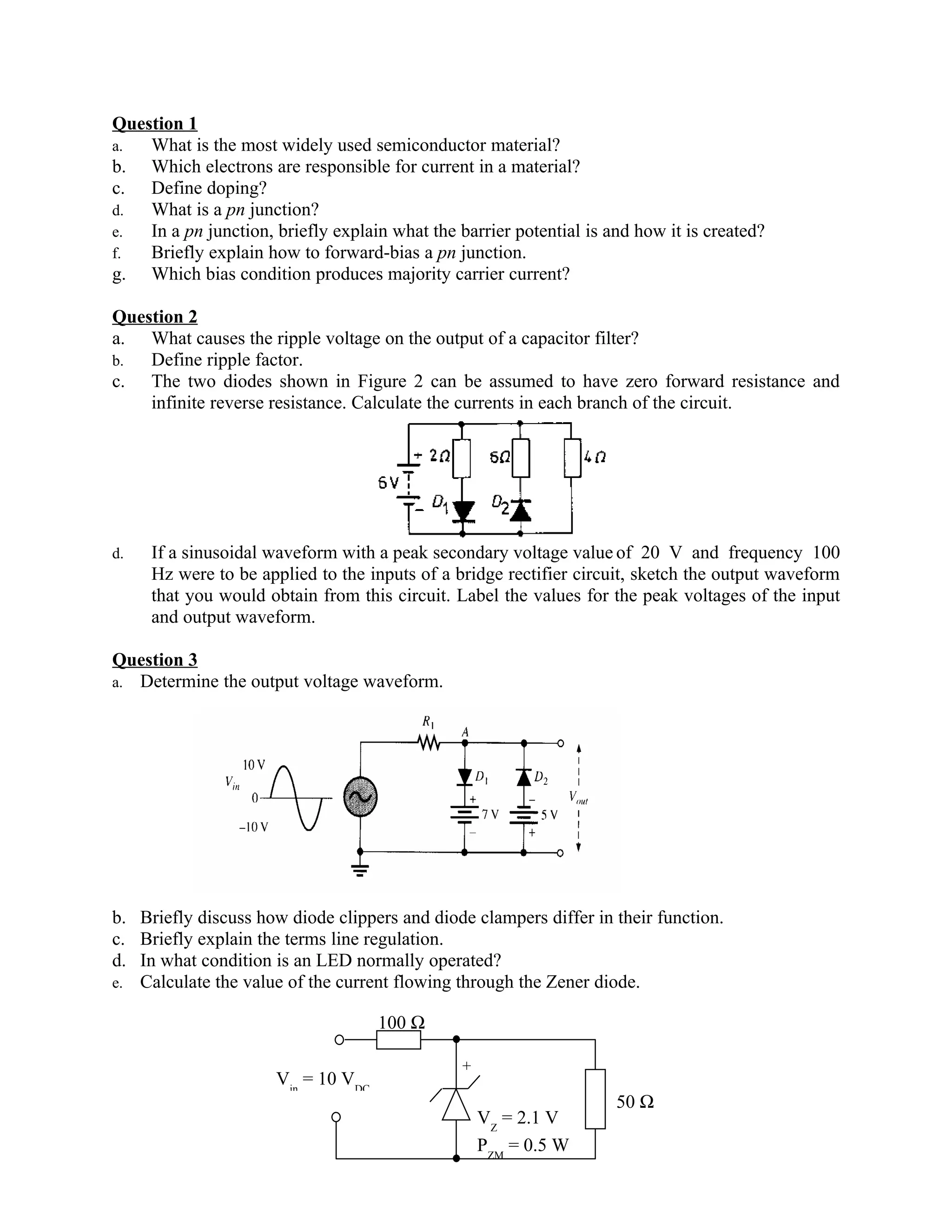
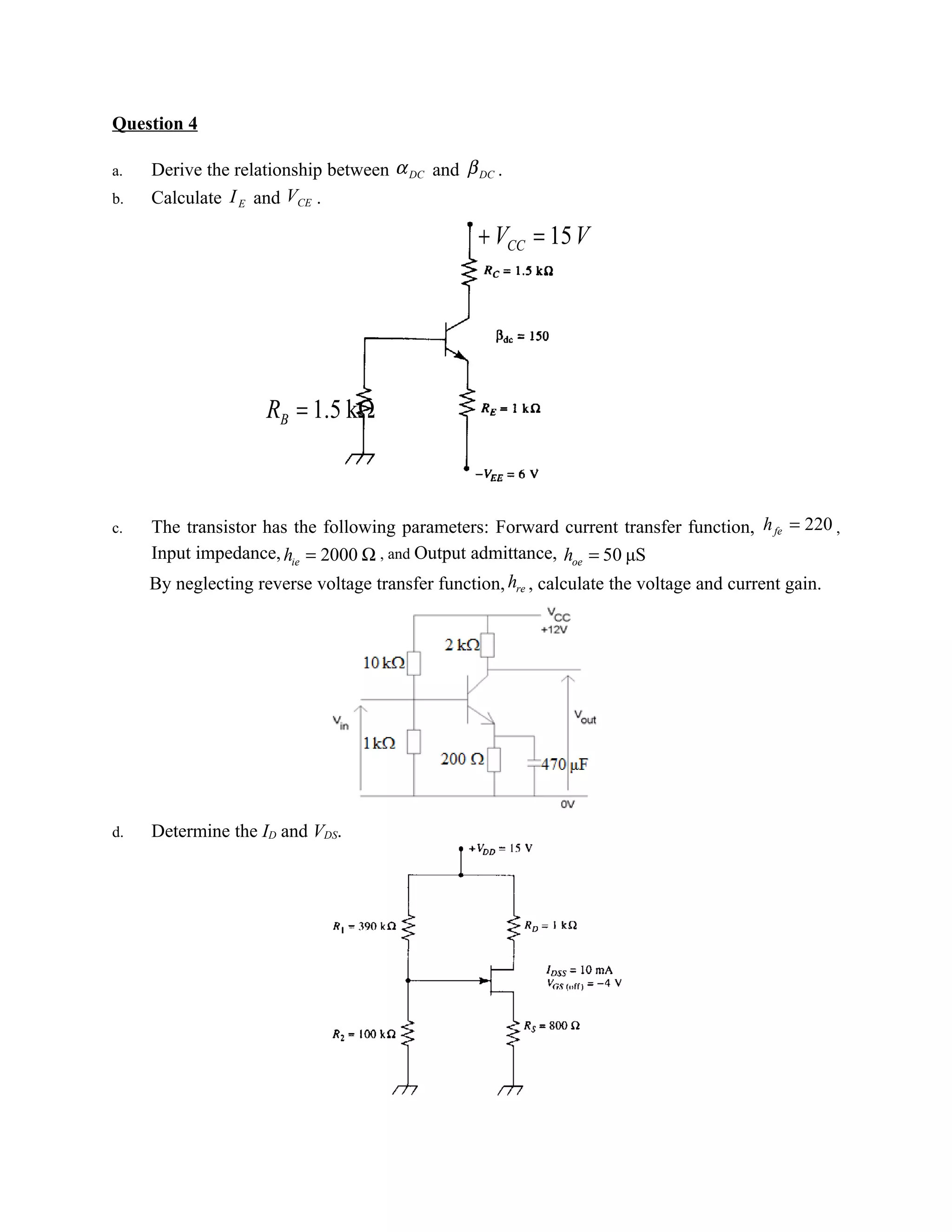
Question 1
a.  What is the most widely used semiconductor material?
b. Which electrons are responsible for current in a material?
c. Define doping?
d.  What is a pn junction?
e.  In a pn junction, briefly explain what the barrier potential is and how it is created?
f.  Briefly explain how to forward-bias a pn junction.
g. Which bias condition produces majority carrier current?

Question 2
a. What causes the ripple voltage on the output of a capacitor filter?
b.  Define ripple factor.
c. The two diodes shown in Figure 2 can be assumed to have zero forward resistance and
    infinite reverse resistance. Calculate the currents in each branch of the circuit.


d.   If a sinusoidal waveform with a peak secondary voltage value of 20 V and frequency 100
     Hz were to be applied to the inputs of a bridge rectifier circuit, sketch the output waveform
     that you would obtain from this circuit. Label the values for the peak voltages of the input
     and output waveform.

Question 3
a. Determine the output voltage waveform.


b. Briefly discuss how diode clippers and diode clampers differ in their function.
c. Briefly explain the terms line regulation.
d. In what condition is an LED normally operated?
e. Calculate the value of the current flowing through the Zener diode.

                                     100 Ω

                                                +
                      Vin = 10 VDC
                                                                     50 Ω
                                                    VZ = 2.1 V
                                                    PZM = 0.5 W
Question 4

a.   Derive the relationship between α DC and β DC .
b.   Calculate I E and VCE .

                                                   + VCC = 15 V


                     RB = 1.5 kΩ


c.   The transistor has the following parameters: Forward current transfer function, h fe = 220 ,
     Input impedance, hie = 2000 Ω , and Output admittance, hoe = 50 μS
     By neglecting reverse voltage transfer function, hre , calculate the voltage and current gain.


d.   Determine the ID and VDS.

Et1 practical final examination

  • 1.
    Question 1 a. What is the most widely used semiconductor material? b. Which electrons are responsible for current in a material? c. Define doping? d. What is a pn junction? e. In a pn junction, briefly explain what the barrier potential is and how it is created? f. Briefly explain how to forward-bias a pn junction. g. Which bias condition produces majority carrier current? Question 2 a. What causes the ripple voltage on the output of a capacitor filter? b. Define ripple factor. c. The two diodes shown in Figure 2 can be assumed to have zero forward resistance and infinite reverse resistance. Calculate the currents in each branch of the circuit. d. If a sinusoidal waveform with a peak secondary voltage value of 20 V and frequency 100 Hz were to be applied to the inputs of a bridge rectifier circuit, sketch the output waveform that you would obtain from this circuit. Label the values for the peak voltages of the input and output waveform. Question 3 a. Determine the output voltage waveform. b. Briefly discuss how diode clippers and diode clampers differ in their function. c. Briefly explain the terms line regulation. d. In what condition is an LED normally operated? e. Calculate the value of the current flowing through the Zener diode. 100 Ω + Vin = 10 VDC 50 Ω VZ = 2.1 V PZM = 0.5 W
  • 2.
    Question 4 a. Derive the relationship between α DC and β DC . b. Calculate I E and VCE . + VCC = 15 V RB = 1.5 kΩ c. The transistor has the following parameters: Forward current transfer function, h fe = 220 , Input impedance, hie = 2000 Ω , and Output admittance, hoe = 50 μS By neglecting reverse voltage transfer function, hre , calculate the voltage and current gain. d. Determine the ID and VDS.