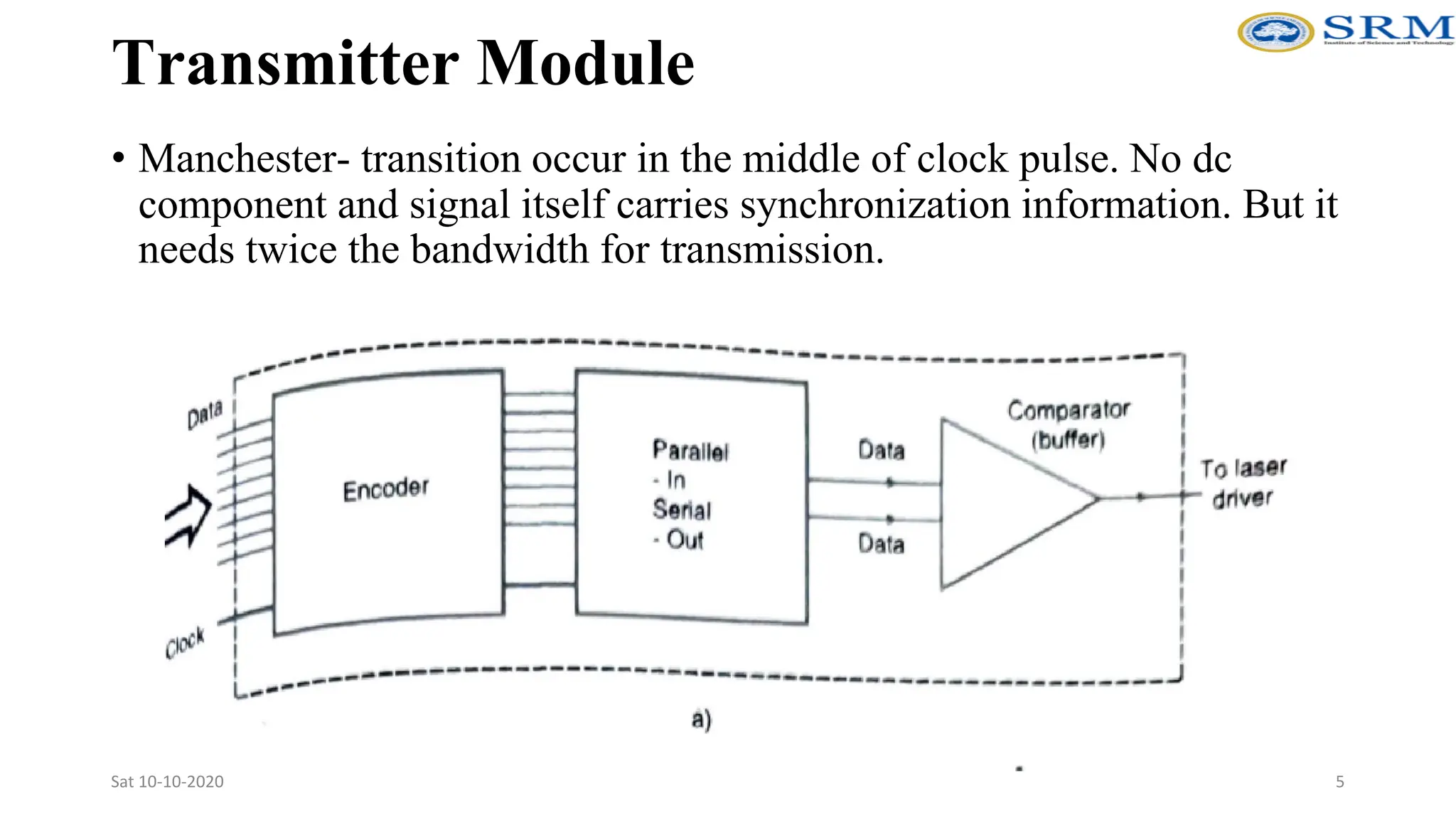
Unit-IV: Optical :-Transmitter &
Receiver
Transmitter Module
• Transmitter is the unit responsible for converting an electrical
information signal into an optical one
• It includes
• Light source
• Coupling optics
• Signalling circuit
• Power control circuit
• Data from outside electronic circuits enter this module along with a
clock signal
• A special unit converts the data into a format suitable to control a laser
diode.
Sat 10-10-2020 2
Transmitter Module
Sat 10-10-2020 3
Transmitter Module
• Laser driver changes the forward current to modulate the output light
radiated by a laser diode
Data conversion unit
• Performs encoding, parallel to serial conversion and reshaping the
electric format of the data
• Encoding means representing data in a physical format (pulses)
• Different line codes used are NRZ, Manchester code, Return to zero
etc.
• NRZ- convenient but has poor transmission capability. Transmitter
and receiver consumes more electric power because of dc power
component
Sat 10-10-2020 4
Transmitter Module
• Manchester- transition occur in the middle of clock pulse. No dc
component and signal itself carries synchronization information. But it
needs twice the bandwidth for transmission.
Sat 10-10-2020 5
Transmitter Module
Sat 10-10-2020 6
Clock Signal
NRZ
Manchester
RZ
Transmitter Module
• Data enters the optical fiber in any one of the codes, but the output of
the transmitter represents logic 1 as a flash of light and 0 as a period of
darkness.
• In parallel to serial conversion, a multiplexer (parallel in serial out) is
used to convert data into serial format.
• For reshaping the electric format, a comparator or buffer can be used
• Comparator compares two signals- data and complementary signal
• If the complementary is higher, output becomes zero
• If data is higher, output becomes equal to Vcc
Sat 10-10-2020 7
Transmitter Module
• Comparator produces high or low voltage in response to input logic 1
or 0
• This circuit has high input impedance which makes it compatible with
the multiplexer
• Buffer is a device that isolates the input from the output and amplifies
the current while transferring the logic signal from the input to the
output unchanged
• Fiber optic transmitter usually utilize emitter coupled logic (ECL)
• ECL include high speed, low noise and the ability to drive low
impendence circuits
• Other logic used- TTL, CMOS
Sat 10-10-2020 8
Transmitter Module
Laser Driver
• Laser driver convert outside voltage in to
current needed to drive the laser
• Driving current has to bias a laser diode to
provide a bias current
• Bias current has to be very stable with
threshold current else error occurs
• Main factor changing threshold current is
temperature
• The feedback signal from the temperature
sensor that reaches the laser driver
through bias control circuit closes the
control loop
Sat 10-10-2020 9
Transmitter Module
• In the figure, current flowing through the resistor (R) depends only on
the input voltage and does not depend on load resistance
• When temperature varies, the feedback signal obtained from a
photodiode helps to stabilize the average output power by changing
the bias current
Modulation Circuit
• Modulation is controlled by changing the driving current from the bias
level to maximum
• When data are represented by a voltage greater than VBB, Q1 conducts
the current and hence laser diode is off
• When data are represented by a voltage less than VBB, Q2 conducts the
current and hence laser diode is on
Sat 10-10-2020 10
Transmitter Module
• VBB at ±400mV and proper design of Q3
keep transistor Q1 and Q2 from saturation
• Signal as small as 800mV switches the gate
from logic 1 to 0
• Switching between transistors Q1 and Q2 occurs
very fast
• Q3 can be controlled by Vdrive
• This is necessary because stabilizing the bias
current is not enough, as this characteristics
actually represents output power only when
no.of 1’s and 0’s are equal
• This is referred as 50% duty cycle
Sat 10-10-2020 11
Transmitter Module
• Another important concern is control of
extinction or on-off ratio
• It is the ration of max to min light
power representing logic 1 and logic 0
• It is controlled by varying current and
can be done automatically
• Given circuit
• Stabilizes the average power by changing
the bias current to compensate for aging
and temperature induced variations
• Compensates for fluctuations in output
light power caused by variations of the
duty cycle when driving changes
Sat 10-10-2020 12
Transmitter Module
Controlling and Monitoring circuits
• Transmitter disable signal allow the user to shut down the transmitter
while keeping the module in the stand by mode
• This can be done by placing high voltage signal at the base of transistor
Q1
• Voltage across R1 and R2 allow the user to receive the bias and
modulation monitoring signals
• Photocurrent produced by PD shows whether LD is working
• Monitoring signal enables the user to troubleshoot the transmitter
• Signal from temperature sensor helps to monitor entire ambient
temperature
• Output also provide alarm to signal if any monitored parameters deviate
Sat 10-10-2020 13
Receiver Configuration
• The three basic stages of the receiver are a photo-detector,
an amplifier, and an equalizer.
• The photo-detector can be either an APD with a mean gain M
or a PIN for which M=1.
• The photodiode has a quantum efficiency η and a capacitance
Cd.
• The detector bias resistor has a resistance Rb which
generates a thermal noise current ib(t).
Receiver Configuration
Fig. Schematic diagram of a typical optical receiver.
Bandwidth of the front end:
CT: Total Capacitance = Cd+Ca
RT: Total Resistance = Rb // Ra
Receiver Configuration
• The amplifier has an input impedance
represented by the parallel combination of a
resistance Ra and a shunt capacitance Ca.
• The amplifying function is represented by the
voltage-controlled current source which is
characterized by a trans conductance gm.
Receiver Configuration
Amplifier Noise Sources:
• The input noise current source ia(t) arises from the
thermal noise of the amplifier input resistance Ra;
• The noise voltage source ea(t) represents the thermal
noise of the amplifier channel.
• The noise sources are assumed to be Gaussian in statistics,
flat in spectrum (which characterizes white noise), and
uncorrelated (statistically independent).
• The noise sources are completely described by their noise
spectral densities SI and SE
Receiver Configuration
The Linear Equalizer:
•The equalizer is normally a linear frequency-
shaping filter that is used to mitigate the effects
of signal distortion and intersymbol interference.
•The equalizer accepts the combined frequency
response of the transmitter, the fiber, and the
receiver, and transforms it into a signal response
suitable for the following signal-processing
electronics.
Receiver Configuration
Optical Receivers
• Optical receivers convert optical signal (light)
to electrical signal (current/voltage)
•Hence referred ‘O/E Converter’
• Photodetector is the fundamental element of
optical receiver, followed by amplifiers and
signal conditioning circuitry
• There are several photodetector types:
•Photodiodes, Phototransistors, Photon
multipliers, Photo-resistors etc.
Receiver Functional Block Diagram
Receiver Types
Low Impedance
•Low
Sensitivity
•Easily Made
•Wide Band
High Impedance
•Requires Equalizer for high BW
•High Sensitivity
•Low Dynamic Range
•Careful Equalizer Placement
Required
Transimpedance
•High Dynamic
Range
•High Sensitivity
•Stability Problems
•Difficult to
equalize
Equivalent Circuits of an Optical Receiver
High Impedance Design Transimpedance Design
Transimpedance with Automatic Gain Control
Receiver Units:
• A receiver is a unit that converts an optical signal into an appropriately formatted electric output signal.
• Receiver converts a stream of light pulses into a stream of electric pulses.
• In transmitters, the light source is either LED or Laser is the heart of these devices, but the properties
of the transmitter depend also on characteristics of the electronics and packaging.
• The same holds true for receivers.
Optical Front end:
• A photodiode along with preamplifiers linked to it is called the receiver’s optical front end.
• The function of this section is to convert light into electric voltage of the required amplitude
• First, photodiode converts light into photo current
• Secondly, preamplifiers converts the photocurrent into voltage, amplifies the signal and presents into
the quantizer.
• In p-i-n photodiode, the thermal noise is the dominant component.
• Noise is inversely proportional to the RL (load resistance)
• As with thermal noise, photodiode’s sensitivity is inversely proportional to the RL
• Hence to decrease the thermal noise (to increase photodiode sensitivity), need to increase the
RL.
• This can be achieved by connecting a photodiode directly to an amplifier
• It gives input impedance of an electronic amplifier is very high.
High impedance design
• On the other hand, bandwidth of photodiode is inversely proportional to the RL (load
resistance).
• Thus, to increase the bandwidth of a receiver, we need to decrease the RL.
• There is a trade-off between Bandwidth and noise of a receiver.
• Preamplifier not only amplify the signal , but also converts current into voltage.
• The conversion function is performed by an amplifier without negative feedback.
Trans impedance design
• Input impedance of an electronic amplifier with negative feedback is called trans impedance (Rz)
• This is the actual RL for the photodiode.
• The output voltage of this preamplifier is given by
• Vout = IP.RZ
• IP is the photocurrent produced by the photodiode
• RZ is the trans impedance of the preamplifier with negative feedback.
• Photodiode is usually integrated with a transimpedance amplifier called PINAMP.
• Even transimpedance design cannot satisfy a variety of requirements that receivers must meet in
today’s field.
• It is critical in fiber optics network applications is the dynamic range which is between the highest and
the lowest input
• Signals at which a preamplifier can operate.
• To further increase the dynamic range of a transimpedance preamplifier, manufacturers include
automatic gain control
• It keeps the amplifier gain to keep the output voltage
stable.
• This means the transimpedance (RZ) is also varied, so that
it is high at a low input signal and low at a high input signal.
Quantizer:
• It consists of three components:
i. Noise Filter --- Improves the signal to noise ratio
ii. Power amplifier/limiter
iii. Decision circuit
• An amplifier/limiter provides power amplification of a signal obtained from a
preamplifier through the noise filter.
• Amplification is high enough, this circuit clips the signal, thus the name limiter.
• Amplification is necessary to attain a signal with enough power to drive the decision
circuit.
• Decision circuit is the unit that determines the logical meaning of the received signal.
• The comparator is used, when the received signal is above threshold, the comparator output is high
(1).
• When the signal is lower than threshold, the comparator output is low (0).
Buffers:
• A buffer transfer a logical signal from the input to the output unchanged but reshapes the
electrical form of this signal.
Clock Recovery:
• Clock recovery extracts timing information from the data stream and helps the decision circuit to
generate clean and reshaped differential data and non-data outputs
• Synchronous digital circuit work under the control of a clock signal.
• The timing signal must be same at the transmitter and receiver ends to synchronize all operations.
• If a receiver clock has a different time, we will experience a data sampling error.
Decision
circuit
LPF
VCO
Phase
detector
Amplifier /
Limiter
Signal Detect:
• It is an alarm circuit
• It monitors the level of the incoming signal and generates a logic low signal when the SNR is not sufficient.
Measurement Standards
Standard
Class
Key
organizations
Functions
Primary NIST (U.S.)
NPL(UK)
PTB(Germany)
• Characterize physical parameters
• Support and accelerate development of
emerging technologies (NIST)
Component
testing
TIA/EIA
ITU-T
IEC
• Define component evaluation tests
• Establish equipment calibration procedures
System
testing
ANSI
IEEE
ITU-T
• Define physical-layer test methods
• Establish measurement procedures for
links and networks
Primary – measuring and characterizing fundamental physical parameters such as attenuation,
bandwidth, mode-field diameter for single mode fibers, and optical power.
Component Testing - relevant tests for fiber optic component performance, and they establish
equipment calibration procedures.
System standards - refer to measurement methods for links and networks.
Basic Test Equipment
• As optical signals pass through the various parts of an optical link, they need to be measured
and characterized in terms of the three fundamental areas of optical power, polarization,
and spectral content.
• The basic pieces of test equipment for carrying out such measurements on optical fiber
components and systems include optical power meters, attenuators, tunable laser sources,
spectrum analyzers, and time-domain reflectometers.
• These come in a variety of capabilities, with sizes ranging from portable, handheld units for
field use to sophisticated briefcase-size bench-top or rack-mountable instruments for
laboratory and manufacturing applications.
• In general, the field units do not need to have the extremely high precision of laboratory
instruments, but they need to be more rugged to maintain reliable and accurate
measurements under extreme environmental conditions of temperature, humidity, dust, and
mechanical stress.
• However, even the handheld equipment for field use has reached a high degree of
sophistication with automated microprocessor-controlled test features and computer
Test equipment Function
Optical power meter Measures total power over a selected
wavelength band
Optical spectrum analyzer (OSA) Measures optical power as a function of
wavelength
Optical power attenuator Reduces power level to prevent instrument
damage or to avoid overload distortion in the
measurements
OTDR (field instrument) Measures attenuation, length, connector /
splice losses, and reflectance levels; helps
locate fiber breaks
Optical power meters
• The function of an optical power meter is to measure total
power over a selected wavelength band.
• Multi wavelength optical power meters using photodetectors
are the most common instrument for measuring optical signal
power levels.
• Usually the meter outputs are given in dBm (where 0dBm 1
mW) or dBμ (where 0 dBμ 1 μW).
• In this versatile instrument, various photodetector heads
having different performance characteristics are available.
• For example, using a Ge photodetector allows a measuring
range of 18 to 60dBm in the 780- to 1600-nm wavelength
band, whereas an InGaAs photodetector allows a measuring
range of 3 to 73dBm in the 840- to 1650-nm wavelength band.
• An RS-232 interface together with application software
allows a user to download measurements and view, export, or
print them in either tabular or graphic form.
• The permanent memory registers can store 512 readings
manually or 400 readings automatically at a programmable
time interval. A handheld model FOT-90A fiber
optic power meter from EXFO.
Optical power attenuators
• In many laboratory or production tests, the characteristics of a
high optical signal level may need to be measured.
• If the level is very high, such as a strong output from an optical
amplifier, the signal may need to be attenuated precisely before
being measured.
• This is done to prevent instrument damage or to avoid overload
distortion in the measurements.
• An optical attenuator allows a user to reduce an optical signal level
up to, for example, 60 dB (a factor of 106) in precise steps at a
specified wavelength, which is usually 1310 or 1550 nm.
• The capabilities of attenuators range from simple tape-cassette-
size devices for quick field measurements that may only need to be
accurate to 0.5 dB to laboratory instruments that have an
attenuation precision of 0.001 dB.
Optical Spectrum Analyzer
• The widespread implementation of WDM systems calls for making optical
spectrum analyses to characterize the spectral behavior of various
telecommunication network elements.
• One widely used instrument for doing this is an optical spectrum analyzer
(OSA), which measures optical power as a function of wavelength.
• The most common implementation uses a diffraction-grating-based optical
filter, which yields wavelength resolutions to less than 0.1 nm.
• Higher wavelength accuracy (0.001nm) is achieved with wavelength meters
based on Michelson interferometry.
• Light emerging from a fiber is collimated by a lens
and is directed onto a diffraction grating that can
be rotated.
• The exit slit selects or filters the spectrum of the
light from the grating.
• Thus, it determines the spectral resolution of the
OSA.
• The term resolution bandwidth describes the width
of this optical filter.
• Typical OSAs have selectable filters ranging from 10
nm down to 0.1 nm.
The operation of a grating-based optical spectrum analyzer.
• The optical filter characteristics determine the dynamic range, which is the ability of the OSA to
simultaneously view large and small signals in the same sweep.
• The bandwidth of the amplifier is a major factor affecting the sensitivity and sweep time of the OSA.
• The photodiode is usually an InGaAs device.
• The OSA normally sweeps across a spectral band, making measurements at
discretely spaced wavelength points.
• This spacing depends on the bandwidth resolution capability of the
instrument and is known as the trace-point spacing.
Optical Time-Domain Reflectometer
• The long-term workhorse instrument in fiber optic systems is the optical
time domain reflectometer (OTDR).
• In addition to locating faults within an optical link, this instrument measures
parameters such as attenuation, length, connector and splice losses, and
reflectance levels.
• A typical OTDR consists of an optical source and receiver, a data acquisition
module, a central processing unit (CPU), an information storage unit for
retaining data either in the internal memory or on an external disk, and a
display.
• As an example of an OTDR instrument, the portable unit can perform tests
for outside plant installation, maintenance, and troubleshooting.
• An OTDR is fundamentally an
optical radar.
• It operates by periodically
launching narrow laser pulses
into one end of a fiber under
test by using either a
directional coupler or a beam
splitter.
• The properties of the optical
fiber link then are determined
by analyzing the amplitude and
temporal characteristics of
the waveform of the
backscattered light.
OTDR trace
Fig: Representative trace of backscattered optical power as displayed on an OTDR screen and the meanings of
various trace features.
Fig. shows a typical trace as would be seen on the display screen of an OTDR.
⮚ The scale of the vertical axis is logarithmic and measures the returning
(back-reflected) signal in decibels.
⮚ The horizontal axis denotes the distance between the instrument and the
measurement point in the fiber.
The backscattered waveform has four distinct features:
• A large initial pulse resulting from Fresnel reflection at the input end of the
fiber.
• A long decaying tail resulting from Rayleigh scattering in the reverse
direction as the input pulse travels along the fiber. In Fig. the different
slopes of the three curves mean that the three fibers have different
attenuations.
• Abrupt shifts in the curve caused by optical loss at joints, at connectors, or
because of sharp bends in the fiber line.
• Positive spikes arising from Fresnel reflection at the far end of the fiber, at
fiber joints, and at fiber imperfections.
• Fresnel reflection and Rayleigh scattering principally produce the
backscattered light.
• Fresnel reflection occurs when light enters a medium having a different
index of refraction.
• For a glass-air interface, when light of power P0 is incident perpendicular
to the interface, the reflected power Pref is
where nfiber and nair are the refractive indices of the fiber core and air,
respectively.
A perfect fiber end reflects about 4 percent of the power incident on it.
However, since fiber ends generally are not polished perfectly and
perpendicular to the fiber axis, the reflected power tends to be much lower
than the maximum possible value.
Two important performance parameters of an OTDR are dynamic range and
measurement range.
• Dynamic range is defined as the difference between the initial
backscattered power level at the front connector and the noise level after 3
min of measurement time.
• It is expressed in decibels of one-way fiber loss.
• Dynamic range provides information on the maximum fiber loss that can be
measured and denotes the time required to measure a given fiber loss.
• Thus it often is used to rank the capabilities of an OTDR.
• A basic limitation of an OTDR is the tradeoff between dynamic range and
resolution. For high spatial resolution, the pulse width has to be as small as
possible.
• However, this reduces the signal-to-noise ratio and thus lowers the dynamic
range. For example, a 100-ns pulse width allows a 24-dB dynamic range,
whereas a 20-μs pulse width increases the dynamic range to 40 dB.
• Measurement range deals with the capability of
identifying events in the link, such as splice points, connection
points, or fiber breaks.
• It is defined as the maximum allowable attenuation between
an OTDR and an event that still enables the OTDR to
accurately measure the event.
• Normally, for definition purposes, a 0.5-dB splice is selected
as the event to be measured.

2. Transmitter and Reciver microwave optical communication

  • 1.
  • 2.
    Transmitter Module • Transmitteris the unit responsible for converting an electrical information signal into an optical one • It includes • Light source • Coupling optics • Signalling circuit • Power control circuit • Data from outside electronic circuits enter this module along with a clock signal • A special unit converts the data into a format suitable to control a laser diode. Sat 10-10-2020 2
  • 3.
  • 4.
    Transmitter Module • Laserdriver changes the forward current to modulate the output light radiated by a laser diode Data conversion unit • Performs encoding, parallel to serial conversion and reshaping the electric format of the data • Encoding means representing data in a physical format (pulses) • Different line codes used are NRZ, Manchester code, Return to zero etc. • NRZ- convenient but has poor transmission capability. Transmitter and receiver consumes more electric power because of dc power component Sat 10-10-2020 4
  • 5.
    Transmitter Module • Manchester-transition occur in the middle of clock pulse. No dc component and signal itself carries synchronization information. But it needs twice the bandwidth for transmission. Sat 10-10-2020 5
  • 6.
    Transmitter Module Sat 10-10-20206 Clock Signal NRZ Manchester RZ
  • 7.
    Transmitter Module • Dataenters the optical fiber in any one of the codes, but the output of the transmitter represents logic 1 as a flash of light and 0 as a period of darkness. • In parallel to serial conversion, a multiplexer (parallel in serial out) is used to convert data into serial format. • For reshaping the electric format, a comparator or buffer can be used • Comparator compares two signals- data and complementary signal • If the complementary is higher, output becomes zero • If data is higher, output becomes equal to Vcc Sat 10-10-2020 7
  • 8.
    Transmitter Module • Comparatorproduces high or low voltage in response to input logic 1 or 0 • This circuit has high input impedance which makes it compatible with the multiplexer • Buffer is a device that isolates the input from the output and amplifies the current while transferring the logic signal from the input to the output unchanged • Fiber optic transmitter usually utilize emitter coupled logic (ECL) • ECL include high speed, low noise and the ability to drive low impendence circuits • Other logic used- TTL, CMOS Sat 10-10-2020 8
  • 9.
    Transmitter Module Laser Driver •Laser driver convert outside voltage in to current needed to drive the laser • Driving current has to bias a laser diode to provide a bias current • Bias current has to be very stable with threshold current else error occurs • Main factor changing threshold current is temperature • The feedback signal from the temperature sensor that reaches the laser driver through bias control circuit closes the control loop Sat 10-10-2020 9
  • 10.
    Transmitter Module • Inthe figure, current flowing through the resistor (R) depends only on the input voltage and does not depend on load resistance • When temperature varies, the feedback signal obtained from a photodiode helps to stabilize the average output power by changing the bias current Modulation Circuit • Modulation is controlled by changing the driving current from the bias level to maximum • When data are represented by a voltage greater than VBB, Q1 conducts the current and hence laser diode is off • When data are represented by a voltage less than VBB, Q2 conducts the current and hence laser diode is on Sat 10-10-2020 10
  • 11.
    Transmitter Module • VBBat ±400mV and proper design of Q3 keep transistor Q1 and Q2 from saturation • Signal as small as 800mV switches the gate from logic 1 to 0 • Switching between transistors Q1 and Q2 occurs very fast • Q3 can be controlled by Vdrive • This is necessary because stabilizing the bias current is not enough, as this characteristics actually represents output power only when no.of 1’s and 0’s are equal • This is referred as 50% duty cycle Sat 10-10-2020 11
  • 12.
    Transmitter Module • Anotherimportant concern is control of extinction or on-off ratio • It is the ration of max to min light power representing logic 1 and logic 0 • It is controlled by varying current and can be done automatically • Given circuit • Stabilizes the average power by changing the bias current to compensate for aging and temperature induced variations • Compensates for fluctuations in output light power caused by variations of the duty cycle when driving changes Sat 10-10-2020 12
  • 13.
    Transmitter Module Controlling andMonitoring circuits • Transmitter disable signal allow the user to shut down the transmitter while keeping the module in the stand by mode • This can be done by placing high voltage signal at the base of transistor Q1 • Voltage across R1 and R2 allow the user to receive the bias and modulation monitoring signals • Photocurrent produced by PD shows whether LD is working • Monitoring signal enables the user to troubleshoot the transmitter • Signal from temperature sensor helps to monitor entire ambient temperature • Output also provide alarm to signal if any monitored parameters deviate Sat 10-10-2020 13
  • 14.
    Receiver Configuration • Thethree basic stages of the receiver are a photo-detector, an amplifier, and an equalizer. • The photo-detector can be either an APD with a mean gain M or a PIN for which M=1. • The photodiode has a quantum efficiency η and a capacitance Cd. • The detector bias resistor has a resistance Rb which generates a thermal noise current ib(t).
  • 15.
    Receiver Configuration Fig. Schematicdiagram of a typical optical receiver. Bandwidth of the front end: CT: Total Capacitance = Cd+Ca RT: Total Resistance = Rb // Ra
  • 16.
    Receiver Configuration • Theamplifier has an input impedance represented by the parallel combination of a resistance Ra and a shunt capacitance Ca. • The amplifying function is represented by the voltage-controlled current source which is characterized by a trans conductance gm.
  • 17.
    Receiver Configuration Amplifier NoiseSources: • The input noise current source ia(t) arises from the thermal noise of the amplifier input resistance Ra; • The noise voltage source ea(t) represents the thermal noise of the amplifier channel. • The noise sources are assumed to be Gaussian in statistics, flat in spectrum (which characterizes white noise), and uncorrelated (statistically independent). • The noise sources are completely described by their noise spectral densities SI and SE
  • 18.
    Receiver Configuration The LinearEqualizer: •The equalizer is normally a linear frequency- shaping filter that is used to mitigate the effects of signal distortion and intersymbol interference. •The equalizer accepts the combined frequency response of the transmitter, the fiber, and the receiver, and transforms it into a signal response suitable for the following signal-processing electronics.
  • 19.
  • 20.
  • 21.
    Optical Receivers • Opticalreceivers convert optical signal (light) to electrical signal (current/voltage) •Hence referred ‘O/E Converter’ • Photodetector is the fundamental element of optical receiver, followed by amplifiers and signal conditioning circuitry • There are several photodetector types: •Photodiodes, Phototransistors, Photon multipliers, Photo-resistors etc.
  • 22.
  • 23.
    Receiver Types Low Impedance •Low Sensitivity •EasilyMade •Wide Band High Impedance •Requires Equalizer for high BW •High Sensitivity •Low Dynamic Range •Careful Equalizer Placement Required Transimpedance •High Dynamic Range •High Sensitivity •Stability Problems •Difficult to equalize
  • 24.
    Equivalent Circuits ofan Optical Receiver High Impedance Design Transimpedance Design Transimpedance with Automatic Gain Control
  • 25.
    Receiver Units: • Areceiver is a unit that converts an optical signal into an appropriately formatted electric output signal. • Receiver converts a stream of light pulses into a stream of electric pulses. • In transmitters, the light source is either LED or Laser is the heart of these devices, but the properties of the transmitter depend also on characteristics of the electronics and packaging. • The same holds true for receivers. Optical Front end: • A photodiode along with preamplifiers linked to it is called the receiver’s optical front end. • The function of this section is to convert light into electric voltage of the required amplitude • First, photodiode converts light into photo current • Secondly, preamplifiers converts the photocurrent into voltage, amplifies the signal and presents into the quantizer.
  • 26.
    • In p-i-nphotodiode, the thermal noise is the dominant component. • Noise is inversely proportional to the RL (load resistance) • As with thermal noise, photodiode’s sensitivity is inversely proportional to the RL • Hence to decrease the thermal noise (to increase photodiode sensitivity), need to increase the RL. • This can be achieved by connecting a photodiode directly to an amplifier • It gives input impedance of an electronic amplifier is very high. High impedance design
  • 27.
    • On theother hand, bandwidth of photodiode is inversely proportional to the RL (load resistance). • Thus, to increase the bandwidth of a receiver, we need to decrease the RL. • There is a trade-off between Bandwidth and noise of a receiver. • Preamplifier not only amplify the signal , but also converts current into voltage. • The conversion function is performed by an amplifier without negative feedback. Trans impedance design
  • 28.
    • Input impedanceof an electronic amplifier with negative feedback is called trans impedance (Rz) • This is the actual RL for the photodiode. • The output voltage of this preamplifier is given by • Vout = IP.RZ • IP is the photocurrent produced by the photodiode • RZ is the trans impedance of the preamplifier with negative feedback. • Photodiode is usually integrated with a transimpedance amplifier called PINAMP. • Even transimpedance design cannot satisfy a variety of requirements that receivers must meet in today’s field. • It is critical in fiber optics network applications is the dynamic range which is between the highest and the lowest input • Signals at which a preamplifier can operate. • To further increase the dynamic range of a transimpedance preamplifier, manufacturers include automatic gain control
  • 29.
    • It keepsthe amplifier gain to keep the output voltage stable. • This means the transimpedance (RZ) is also varied, so that it is high at a low input signal and low at a high input signal. Quantizer: • It consists of three components: i. Noise Filter --- Improves the signal to noise ratio ii. Power amplifier/limiter iii. Decision circuit • An amplifier/limiter provides power amplification of a signal obtained from a preamplifier through the noise filter. • Amplification is high enough, this circuit clips the signal, thus the name limiter. • Amplification is necessary to attain a signal with enough power to drive the decision circuit.
  • 30.
    • Decision circuitis the unit that determines the logical meaning of the received signal. • The comparator is used, when the received signal is above threshold, the comparator output is high (1). • When the signal is lower than threshold, the comparator output is low (0). Buffers: • A buffer transfer a logical signal from the input to the output unchanged but reshapes the electrical form of this signal. Clock Recovery: • Clock recovery extracts timing information from the data stream and helps the decision circuit to generate clean and reshaped differential data and non-data outputs • Synchronous digital circuit work under the control of a clock signal. • The timing signal must be same at the transmitter and receiver ends to synchronize all operations. • If a receiver clock has a different time, we will experience a data sampling error.
  • 31.
    Decision circuit LPF VCO Phase detector Amplifier / Limiter Signal Detect: •It is an alarm circuit • It monitors the level of the incoming signal and generates a logic low signal when the SNR is not sufficient.
  • 32.
    Measurement Standards Standard Class Key organizations Functions Primary NIST(U.S.) NPL(UK) PTB(Germany) • Characterize physical parameters • Support and accelerate development of emerging technologies (NIST) Component testing TIA/EIA ITU-T IEC • Define component evaluation tests • Establish equipment calibration procedures System testing ANSI IEEE ITU-T • Define physical-layer test methods • Establish measurement procedures for links and networks Primary – measuring and characterizing fundamental physical parameters such as attenuation, bandwidth, mode-field diameter for single mode fibers, and optical power. Component Testing - relevant tests for fiber optic component performance, and they establish equipment calibration procedures. System standards - refer to measurement methods for links and networks.
  • 33.
    Basic Test Equipment •As optical signals pass through the various parts of an optical link, they need to be measured and characterized in terms of the three fundamental areas of optical power, polarization, and spectral content. • The basic pieces of test equipment for carrying out such measurements on optical fiber components and systems include optical power meters, attenuators, tunable laser sources, spectrum analyzers, and time-domain reflectometers. • These come in a variety of capabilities, with sizes ranging from portable, handheld units for field use to sophisticated briefcase-size bench-top or rack-mountable instruments for laboratory and manufacturing applications. • In general, the field units do not need to have the extremely high precision of laboratory instruments, but they need to be more rugged to maintain reliable and accurate measurements under extreme environmental conditions of temperature, humidity, dust, and mechanical stress. • However, even the handheld equipment for field use has reached a high degree of sophistication with automated microprocessor-controlled test features and computer
  • 34.
    Test equipment Function Opticalpower meter Measures total power over a selected wavelength band Optical spectrum analyzer (OSA) Measures optical power as a function of wavelength Optical power attenuator Reduces power level to prevent instrument damage or to avoid overload distortion in the measurements OTDR (field instrument) Measures attenuation, length, connector / splice losses, and reflectance levels; helps locate fiber breaks
  • 35.
    Optical power meters •The function of an optical power meter is to measure total power over a selected wavelength band. • Multi wavelength optical power meters using photodetectors are the most common instrument for measuring optical signal power levels. • Usually the meter outputs are given in dBm (where 0dBm 1 mW) or dBμ (where 0 dBμ 1 μW). • In this versatile instrument, various photodetector heads having different performance characteristics are available. • For example, using a Ge photodetector allows a measuring range of 18 to 60dBm in the 780- to 1600-nm wavelength band, whereas an InGaAs photodetector allows a measuring range of 3 to 73dBm in the 840- to 1650-nm wavelength band. • An RS-232 interface together with application software allows a user to download measurements and view, export, or print them in either tabular or graphic form. • The permanent memory registers can store 512 readings manually or 400 readings automatically at a programmable time interval. A handheld model FOT-90A fiber optic power meter from EXFO.
  • 36.
    Optical power attenuators •In many laboratory or production tests, the characteristics of a high optical signal level may need to be measured. • If the level is very high, such as a strong output from an optical amplifier, the signal may need to be attenuated precisely before being measured. • This is done to prevent instrument damage or to avoid overload distortion in the measurements. • An optical attenuator allows a user to reduce an optical signal level up to, for example, 60 dB (a factor of 106) in precise steps at a specified wavelength, which is usually 1310 or 1550 nm. • The capabilities of attenuators range from simple tape-cassette- size devices for quick field measurements that may only need to be accurate to 0.5 dB to laboratory instruments that have an attenuation precision of 0.001 dB.
  • 37.
    Optical Spectrum Analyzer •The widespread implementation of WDM systems calls for making optical spectrum analyses to characterize the spectral behavior of various telecommunication network elements. • One widely used instrument for doing this is an optical spectrum analyzer (OSA), which measures optical power as a function of wavelength. • The most common implementation uses a diffraction-grating-based optical filter, which yields wavelength resolutions to less than 0.1 nm. • Higher wavelength accuracy (0.001nm) is achieved with wavelength meters based on Michelson interferometry.
  • 38.
    • Light emergingfrom a fiber is collimated by a lens and is directed onto a diffraction grating that can be rotated. • The exit slit selects or filters the spectrum of the light from the grating. • Thus, it determines the spectral resolution of the OSA. • The term resolution bandwidth describes the width of this optical filter. • Typical OSAs have selectable filters ranging from 10 nm down to 0.1 nm. The operation of a grating-based optical spectrum analyzer. • The optical filter characteristics determine the dynamic range, which is the ability of the OSA to simultaneously view large and small signals in the same sweep. • The bandwidth of the amplifier is a major factor affecting the sensitivity and sweep time of the OSA. • The photodiode is usually an InGaAs device.
  • 39.
    • The OSAnormally sweeps across a spectral band, making measurements at discretely spaced wavelength points. • This spacing depends on the bandwidth resolution capability of the instrument and is known as the trace-point spacing.
  • 40.
    Optical Time-Domain Reflectometer •The long-term workhorse instrument in fiber optic systems is the optical time domain reflectometer (OTDR). • In addition to locating faults within an optical link, this instrument measures parameters such as attenuation, length, connector and splice losses, and reflectance levels. • A typical OTDR consists of an optical source and receiver, a data acquisition module, a central processing unit (CPU), an information storage unit for retaining data either in the internal memory or on an external disk, and a display. • As an example of an OTDR instrument, the portable unit can perform tests for outside plant installation, maintenance, and troubleshooting.
  • 41.
    • An OTDRis fundamentally an optical radar. • It operates by periodically launching narrow laser pulses into one end of a fiber under test by using either a directional coupler or a beam splitter. • The properties of the optical fiber link then are determined by analyzing the amplitude and temporal characteristics of the waveform of the backscattered light.
  • 42.
    OTDR trace Fig: Representativetrace of backscattered optical power as displayed on an OTDR screen and the meanings of various trace features.
  • 43.
    Fig. shows atypical trace as would be seen on the display screen of an OTDR. ⮚ The scale of the vertical axis is logarithmic and measures the returning (back-reflected) signal in decibels. ⮚ The horizontal axis denotes the distance between the instrument and the measurement point in the fiber. The backscattered waveform has four distinct features: • A large initial pulse resulting from Fresnel reflection at the input end of the fiber. • A long decaying tail resulting from Rayleigh scattering in the reverse direction as the input pulse travels along the fiber. In Fig. the different slopes of the three curves mean that the three fibers have different attenuations. • Abrupt shifts in the curve caused by optical loss at joints, at connectors, or because of sharp bends in the fiber line. • Positive spikes arising from Fresnel reflection at the far end of the fiber, at fiber joints, and at fiber imperfections.
  • 44.
    • Fresnel reflectionand Rayleigh scattering principally produce the backscattered light. • Fresnel reflection occurs when light enters a medium having a different index of refraction. • For a glass-air interface, when light of power P0 is incident perpendicular to the interface, the reflected power Pref is where nfiber and nair are the refractive indices of the fiber core and air, respectively. A perfect fiber end reflects about 4 percent of the power incident on it. However, since fiber ends generally are not polished perfectly and perpendicular to the fiber axis, the reflected power tends to be much lower than the maximum possible value.
  • 45.
    Two important performanceparameters of an OTDR are dynamic range and measurement range. • Dynamic range is defined as the difference between the initial backscattered power level at the front connector and the noise level after 3 min of measurement time. • It is expressed in decibels of one-way fiber loss. • Dynamic range provides information on the maximum fiber loss that can be measured and denotes the time required to measure a given fiber loss. • Thus it often is used to rank the capabilities of an OTDR. • A basic limitation of an OTDR is the tradeoff between dynamic range and resolution. For high spatial resolution, the pulse width has to be as small as possible. • However, this reduces the signal-to-noise ratio and thus lowers the dynamic range. For example, a 100-ns pulse width allows a 24-dB dynamic range, whereas a 20-μs pulse width increases the dynamic range to 40 dB.
  • 46.
    • Measurement rangedeals with the capability of identifying events in the link, such as splice points, connection points, or fiber breaks. • It is defined as the maximum allowable attenuation between an OTDR and an event that still enables the OTDR to accurately measure the event. • Normally, for definition purposes, a 0.5-dB splice is selected as the event to be measured.