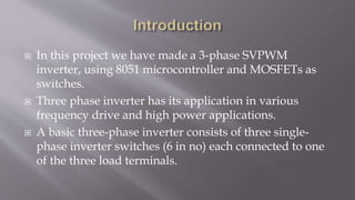
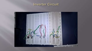
The document summarizes a student project to design and implement a 3-phase inverter using an 8051 microcontroller and MOSFET switches. Key aspects include:
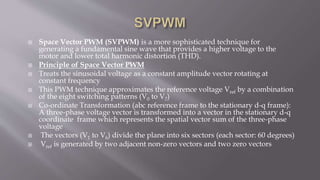
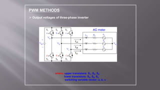
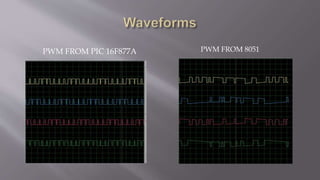
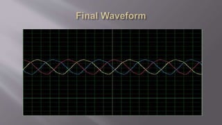
1) The project uses Space Vector PWM (SVPWM) technique to generate sine waves with high voltage and low harmonic distortion for driving AC motors.
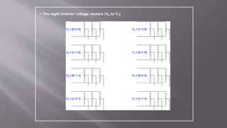
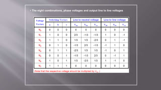
2) SVPWM approximates the reference voltage using combinations of the eight switching vector patterns.
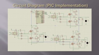
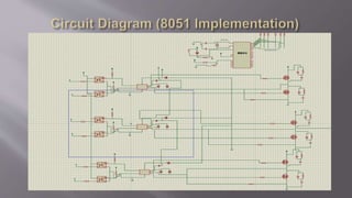
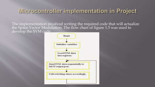
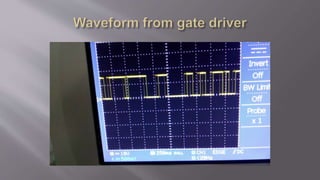
3) An 8051 microcontroller was programmed to implement the SVPWM algorithm and control the MOSFET switches to generate the three-phase output voltages.
4) The students gained experience with electrical simulation tools and building the circuit with components.


![[Deck] What's New in Spark-Iceberg Integration via DSV2.pptx](https://cdn.slidesharecdn.com/ss_thumbnails/deckwhatsnewinspark-icebergintegrationviadsv2-260210005337-25955b12-thumbnail.jpg?width=640&height=640&fit=bounds)