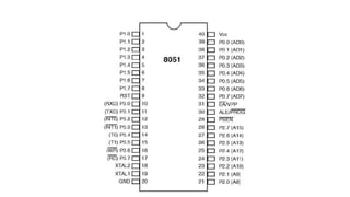
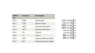
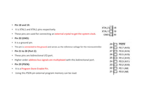
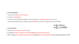
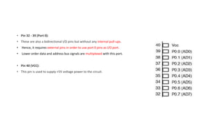
Pin diagram of 8051
Mrs. Hezal Lopes
Assistant Professor
DJSCE,Vile Parle(W)
• Pin configuration of 8051
• The pin diagram of 8051 microcontroller consists of 40 pins as given below:
• Pin 1-8 (Port1):
• These are 8-bit bidirectional I/O port with internal pull-up resisters.
• It does not perform any task; it is just an I/O port
• Pin 9 (RST):
• It is a Reset input pin which is used to reset the microcontroller to its initial position.
• Pin 10 to 17 (Port 3):
• It is also an 8-bit bidirectional I/O port with internal pull-up resisters.
• Additionally, it performs some special functions:
PORT 3
Pin
Function Description
P3.0 RXD Serial Input
P3.1 TXD Serial Output
P3.2 INT0 External Interrupt 0
P3.3 INT1 External Interrupt 1
P3.4 T0 Timer 0
P3.5 T1 Timer 1
P3.6 WR External Memory Write
P3.7 RD External Memory Read
• Pin 18 and 19:
• It is XTAL1 and XTAL1 pins respectively.
• These pins are used for connecting an external crystal to get the system clock.
• Pin 20 (GND):
• It is a ground pin.
• This pin is connected to the ground and serves as the reference voltage for the microcontroller.
• Pin 21 to 28 (Port 2):
• These pins are bidirectional I/O port.
• Higher order address bus signals are multiplexed with this bidirectional port.
• Pin 29 (PSEN):
• It is a Program Store Enable Pin.
• Using this PSEN pin external program memory can be read.
• Pin 30 (ALE/PROG):
• This pin is the Address Latch Enable pin.
• It is input, active-high pin.
• This pin is used to distinguish between memory chips when multiple memory chips are used.
• During flash programming i.e. Programming of EPROM, this pin acts as program pulse input (PROG).
• Pin 31 (EA/VPP):
• Named as external Access Enable Pin (EA).
• It is used to enable or disable the external (ROM)program memory interfacing.
• VPP: It receives 12 V programming enable voltage during flash memory programming for chips that requires 12 V VPP.
• Pin 32 - 39 (Port 0):
• These are also a bidirectional I/O pins but without any internal pull-ups.
• Hence, it requires external pins in order to use port 0 pins as I/O port.
• Lower order data and address bus signals are multiplexed with this port.
• Pin 40 (VCC):
• This pin is used to supply +5V voltage power to the circuit.
Thank You

Pin configuration of 8051 Microcontroller.pdf

  • 1.
    Pin diagram of8051 Mrs. Hezal Lopes Assistant Professor DJSCE,Vile Parle(W)
  • 2.
  • 4.
    • The pindiagram of 8051 microcontroller consists of 40 pins as given below: • Pin 1-8 (Port1): • These are 8-bit bidirectional I/O port with internal pull-up resisters. • It does not perform any task; it is just an I/O port • Pin 9 (RST): • It is a Reset input pin which is used to reset the microcontroller to its initial position. • Pin 10 to 17 (Port 3): • It is also an 8-bit bidirectional I/O port with internal pull-up resisters. • Additionally, it performs some special functions:
  • 5.
    PORT 3 Pin Function Description P3.0RXD Serial Input P3.1 TXD Serial Output P3.2 INT0 External Interrupt 0 P3.3 INT1 External Interrupt 1 P3.4 T0 Timer 0 P3.5 T1 Timer 1 P3.6 WR External Memory Write P3.7 RD External Memory Read
  • 6.
    • Pin 18and 19: • It is XTAL1 and XTAL1 pins respectively. • These pins are used for connecting an external crystal to get the system clock. • Pin 20 (GND): • It is a ground pin. • This pin is connected to the ground and serves as the reference voltage for the microcontroller. • Pin 21 to 28 (Port 2): • These pins are bidirectional I/O port. • Higher order address bus signals are multiplexed with this bidirectional port. • Pin 29 (PSEN): • It is a Program Store Enable Pin. • Using this PSEN pin external program memory can be read.
  • 7.
    • Pin 30(ALE/PROG): • This pin is the Address Latch Enable pin. • It is input, active-high pin. • This pin is used to distinguish between memory chips when multiple memory chips are used. • During flash programming i.e. Programming of EPROM, this pin acts as program pulse input (PROG). • Pin 31 (EA/VPP): • Named as external Access Enable Pin (EA). • It is used to enable or disable the external (ROM)program memory interfacing. • VPP: It receives 12 V programming enable voltage during flash memory programming for chips that requires 12 V VPP.
  • 8.
    • Pin 32- 39 (Port 0): • These are also a bidirectional I/O pins but without any internal pull-ups. • Hence, it requires external pins in order to use port 0 pins as I/O port. • Lower order data and address bus signals are multiplexed with this port. • Pin 40 (VCC): • This pin is used to supply +5V voltage power to the circuit.
  • 9.