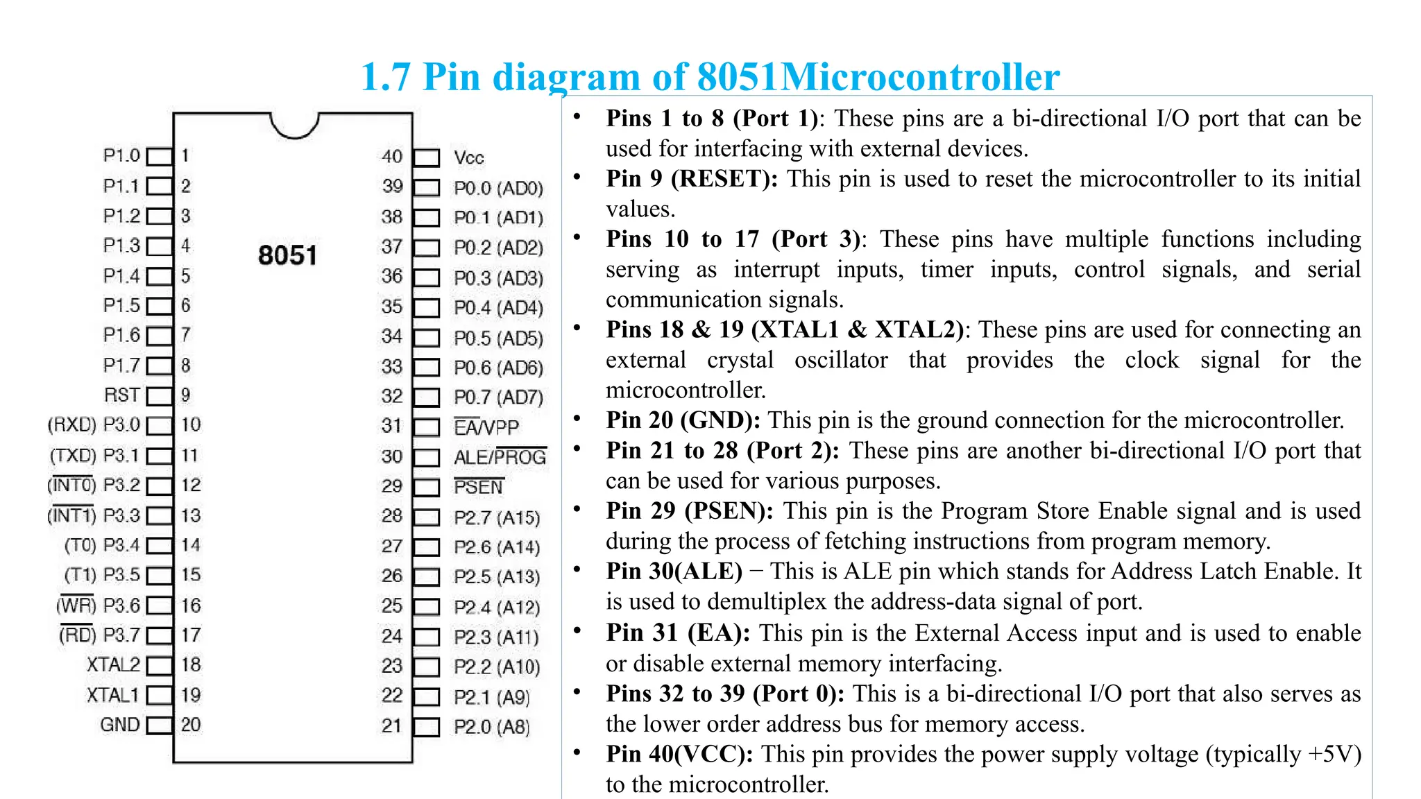
1.7 Pin diagramof 8051Microcontroller
• Pins 1 to 8 (Port 1): These pins are a bi-directional I/O port that can be
used for interfacing with external devices.
• Pin 9 (RESET): This pin is used to reset the microcontroller to its initial
values.
• Pins 10 to 17 (Port 3): These pins have multiple functions including
serving as interrupt inputs, timer inputs, control signals, and serial
communication signals.
• Pins 18 & 19 (XTAL1 & XTAL2): These pins are used for connecting an
external crystal oscillator that provides the clock signal for the
microcontroller.
• Pin 20 (GND): This pin is the ground connection for the microcontroller.
• Pin 21 to 28 (Port 2): These pins are another bi-directional I/O port that
can be used for various purposes.
• Pin 29 (PSEN): This pin is the Program Store Enable signal and is used
during the process of fetching instructions from program memory.
• Pin 30(ALE) − This is ALE pin which stands for Address Latch Enable. It
is used to demultiplex the address-data signal of port.
• Pin 31 (EA): This pin is the External Access input and is used to enable
or disable external memory interfacing.
• Pins 32 to 39 (Port 0): This is a bi-directional I/O port that also serves as
the lower order address bus for memory access.
• Pin 40(VCC): This pin provides the power supply voltage (typically +5V)
to the microcontroller.
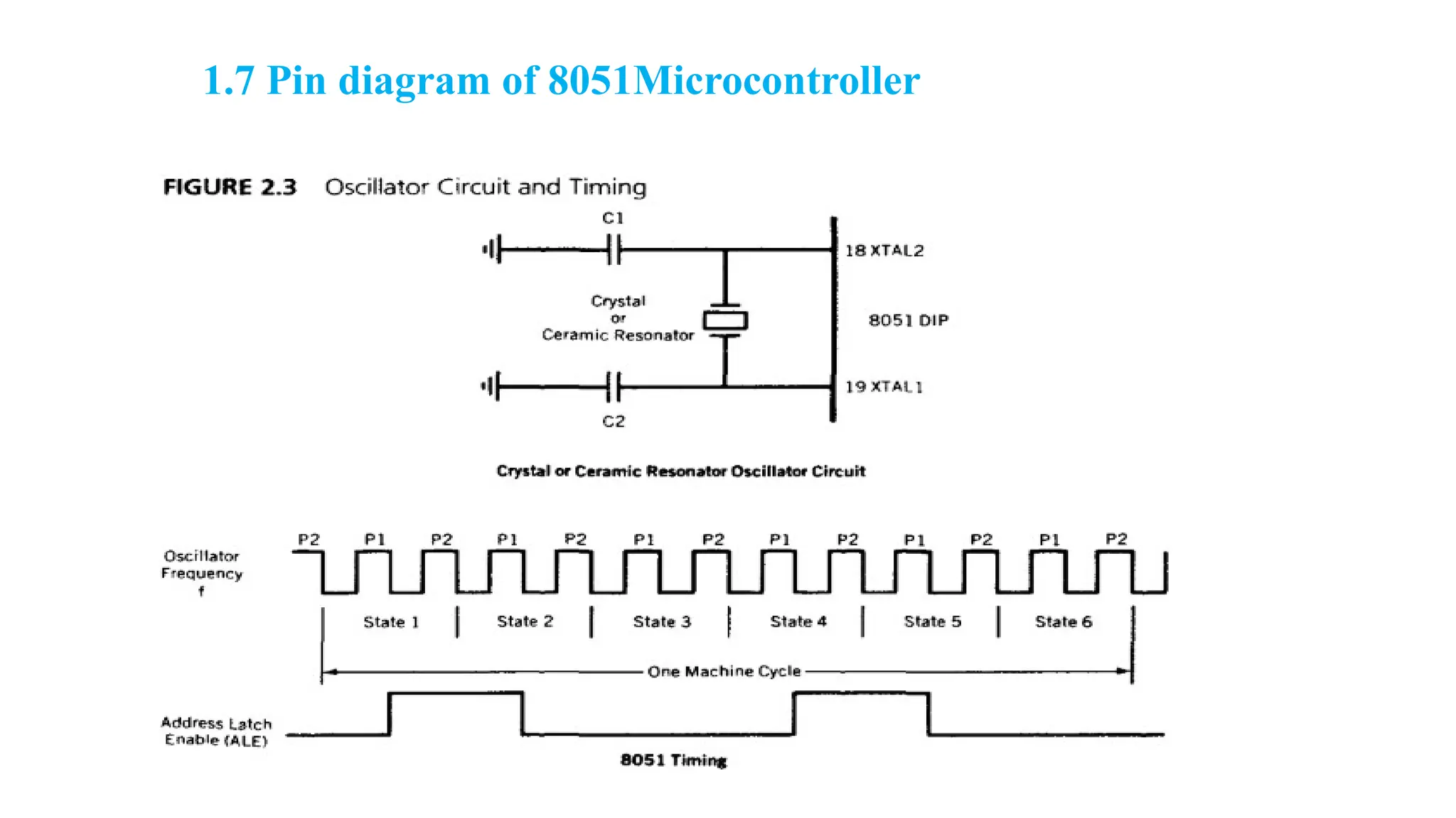
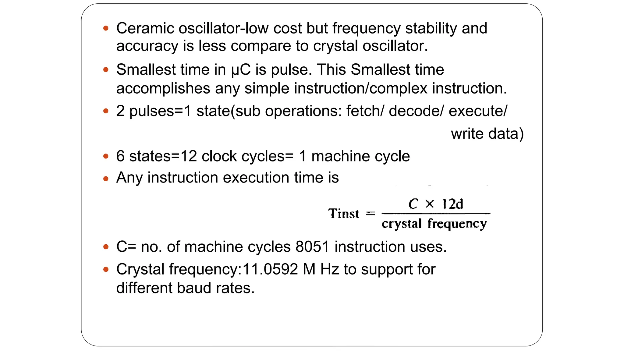
Ceramic oscillator-low costbut frequency stability and
accuracy is less compare to crystal oscillator.
Smallest time in μC is pulse. This Smallest time
accomplishes any simple instruction/complex instruction.
2 pulses=1 state(sub operations: fetch/ decode/ execute/
write data)
6 states=12 clock cycles= 1 machine cycle
Any instruction execution time is
C= no. of machine cycles 8051 instruction uses.
Crystal frequency:11.0592 M Hz to support for
different baud rates.
6.
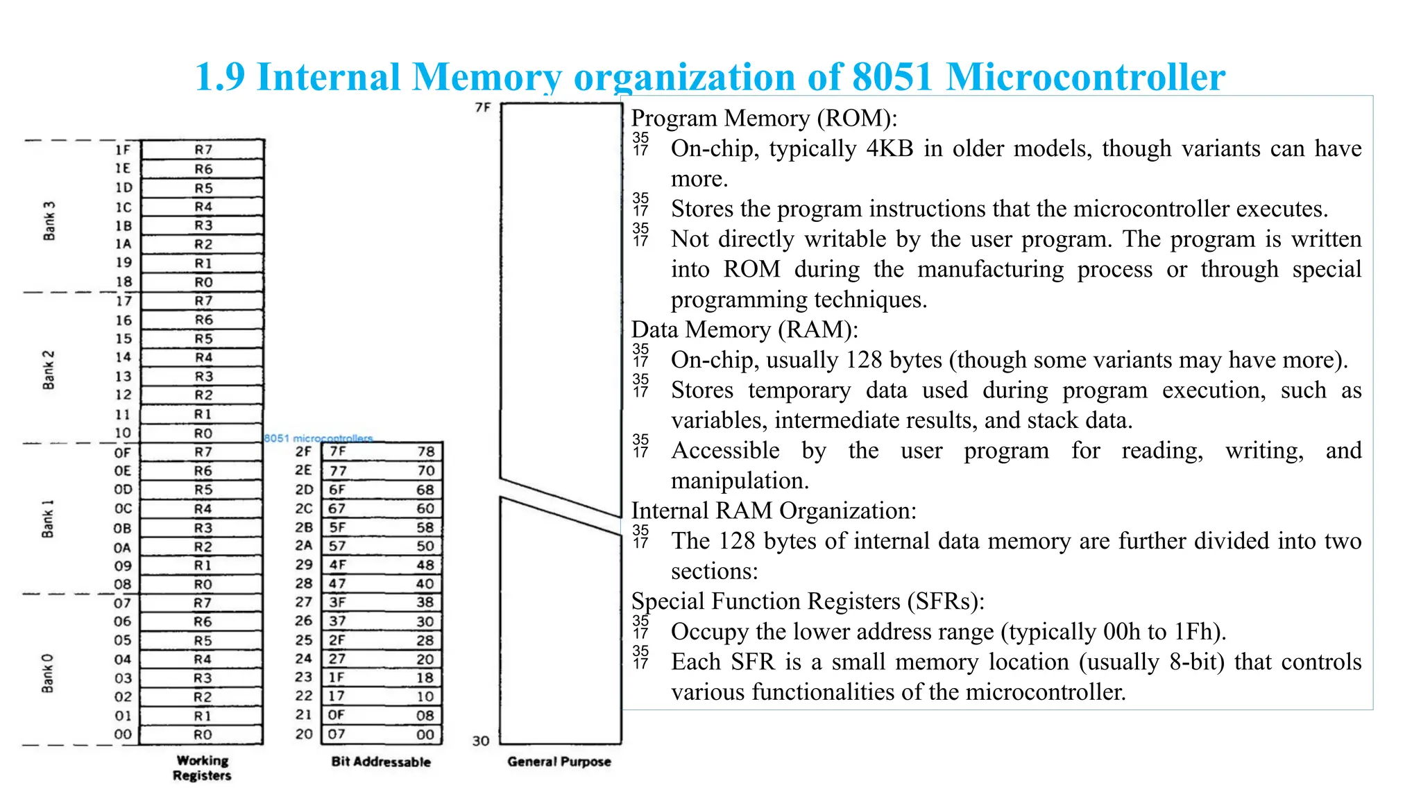
1.9 Internal Memoryorganization of 8051 Microcontroller
Program Memory (ROM):
On-chip, typically 4KB in older models, though variants can have
more.
Stores the program instructions that the microcontroller executes.
Not directly writable by the user program. The program is written
into ROM during the manufacturing process or through special
programming techniques.
Data Memory (RAM):
On-chip, usually 128 bytes (though some variants may have more).
Stores temporary data used during program execution, such as
variables, intermediate results, and stack data.
Accessible by the user program for reading, writing, and
manipulation.
Internal RAM Organization:
The 128 bytes of internal data memory are further divided into two
sections:
Special Function Registers (SFRs):
Occupy the lower address range (typically 00h to 1Fh).
Each SFR is a small memory location (usually 8-bit) that controls
various functionalities of the microcontroller.
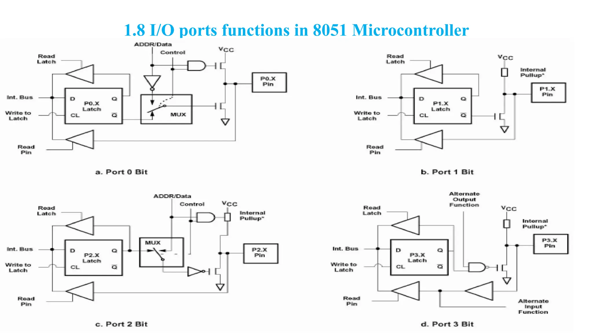
1.8 I/O portsfunctions in 8051 Microcontroller
• Pin configuration, i.e. the pin can be configured as 1 for input and 0 for
output as per the logic state.
• Input/Output (I/O) pin − All the circuits within the microcontroller must
be connected to one of its pins except P0 port because it does not
have pull-up resistors built-in.
• Input pin − Logic 1 is applied to a bit of the P register. The output FE
transistor is turned off and the other pin remains connected to the
power supply voltage over a pull-up resistor of high resistance.
9.
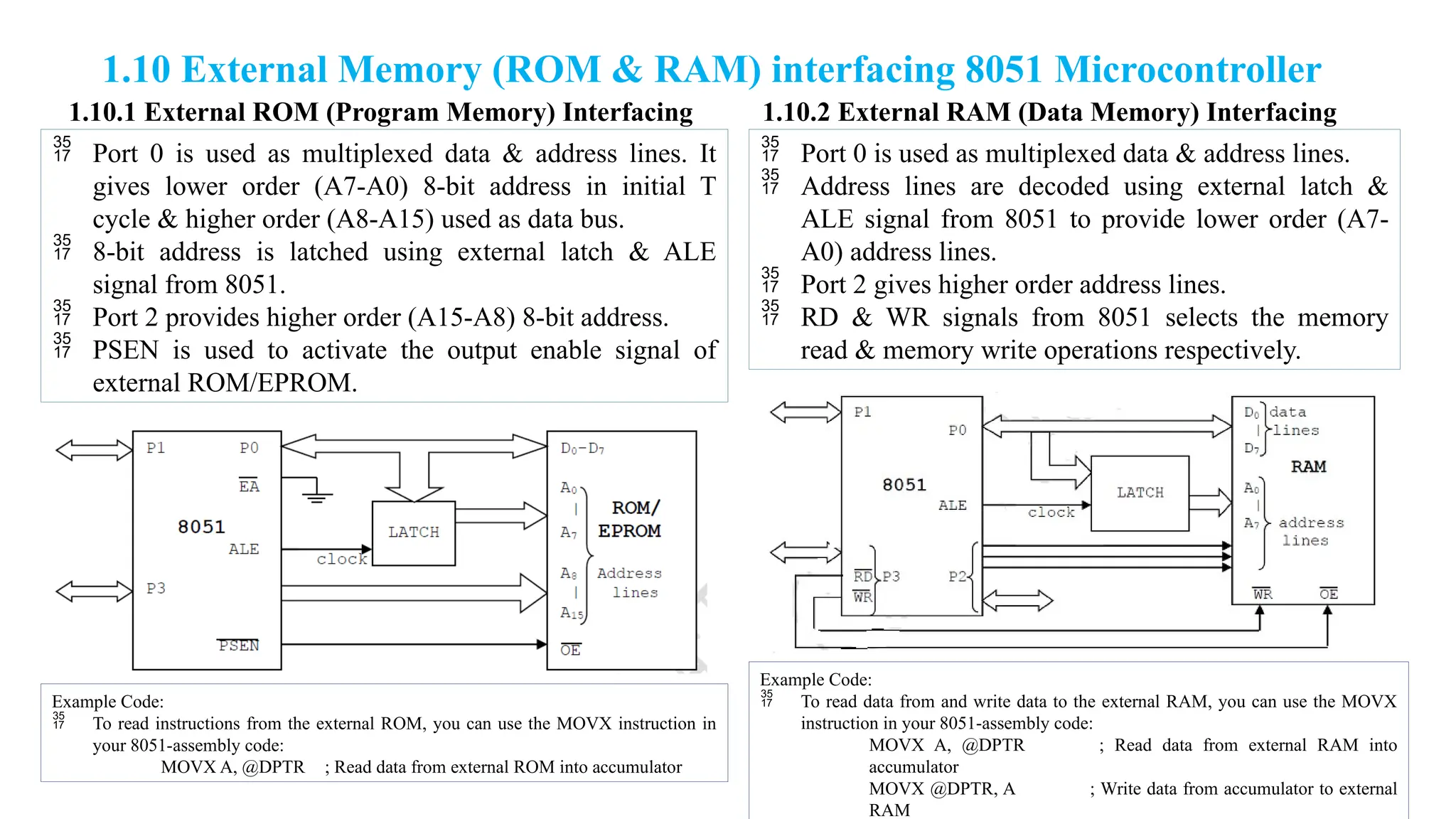
1.10 External Memory(ROM & RAM) interfacing 8051 Microcontroller
1.10.1 External ROM (Program Memory) Interfacing
Port 0 is used as multiplexed data & address lines. It
gives lower order (A7-A0) 8-bit address in initial T
cycle & higher order (A8-A15) used as data bus.
8-bit address is latched using external latch & ALE
signal from 8051.
Port 2 provides higher order (A15-A8) 8-bit address.
PSEN is used to activate the output enable signal of
external ROM/EPROM.
1.10.2 External RAM (Data Memory) Interfacing
Port 0 is used as multiplexed data & address lines.
Address lines are decoded using external latch &
ALE signal from 8051 to provide lower order (A7-
A0) address lines.
Port 2 gives higher order address lines.
RD & WR signals from 8051 selects the memory
read & memory write operations respectively.
Example Code:
To read instructions from the external ROM, you can use the MOVX instruction in
your 8051-assembly code:
MOVX A, @DPTR ; Read data from external ROM into accumulator
Example Code:
To read data from and write data to the external RAM, you can use the MOVX
instruction in your 8051-assembly code:
MOVX A, @DPTR ; Read data from external RAM into
accumulator
MOVX @DPTR, A ; Write data from accumulator to external
RAM