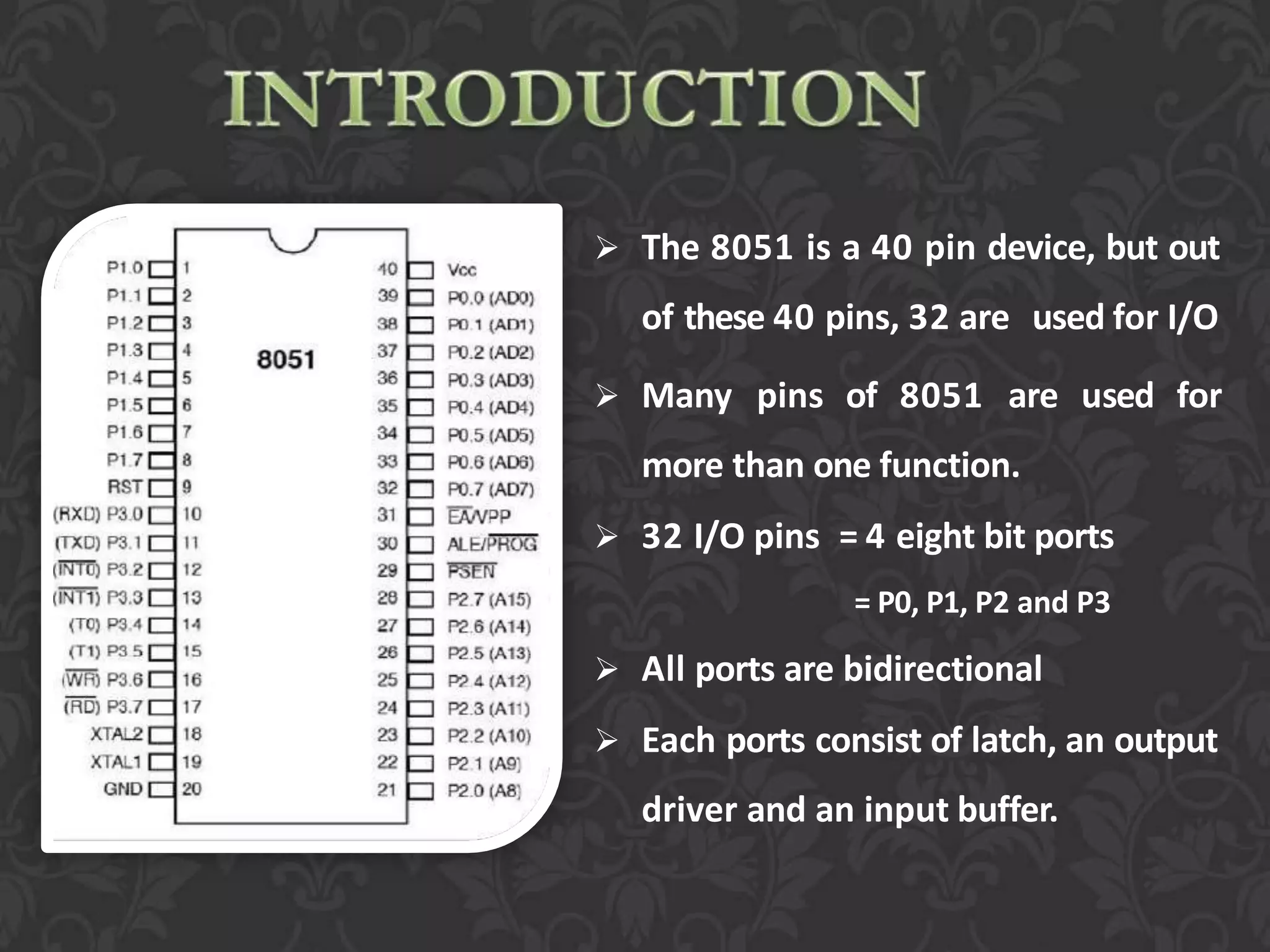
 The 8051 is a 40 pin device, but out
of these 40 pins, 32 are used for I/O
 Many pins of 8051 are used for
more than one function.
 32 I/O pins = 4 eight bit ports
= P0, P1, P2 and P3
 All ports are bidirectional
 Each ports consist of latch, an output
driver and an input buffer.
 40 pin DIP
 +5 volts DC.
 Among the 40 pins , 32 pins = four parallel ports P0, P1, P2
and P3 . Remaining pins are VCC, GND, XTAL1, XTAL2, RST, EA ,
PSEN, ALE.
 P0.0- P0.7(AD0-AD7) (32-39)
 The port 0 pins multiplexed with (low order byte) Address/data
pins .
 If the microcontroller is accessing external memory, these pins
will act as address/data pins otherwise, they are used for Port 0
pins.
 P1.0- P1.7 (1 – 8)
 These 8-pins are dedicated for Port 1 to perform input or
output port operations.
 P2.0- P2.7(A8-A15) (21-28)
 The port 2 pins are multiplexed with the higher order
address pins .
 When the microcontroller is accessing external memory
these pins provide the higher order address byte
otherwise they act as Port 2 pins.
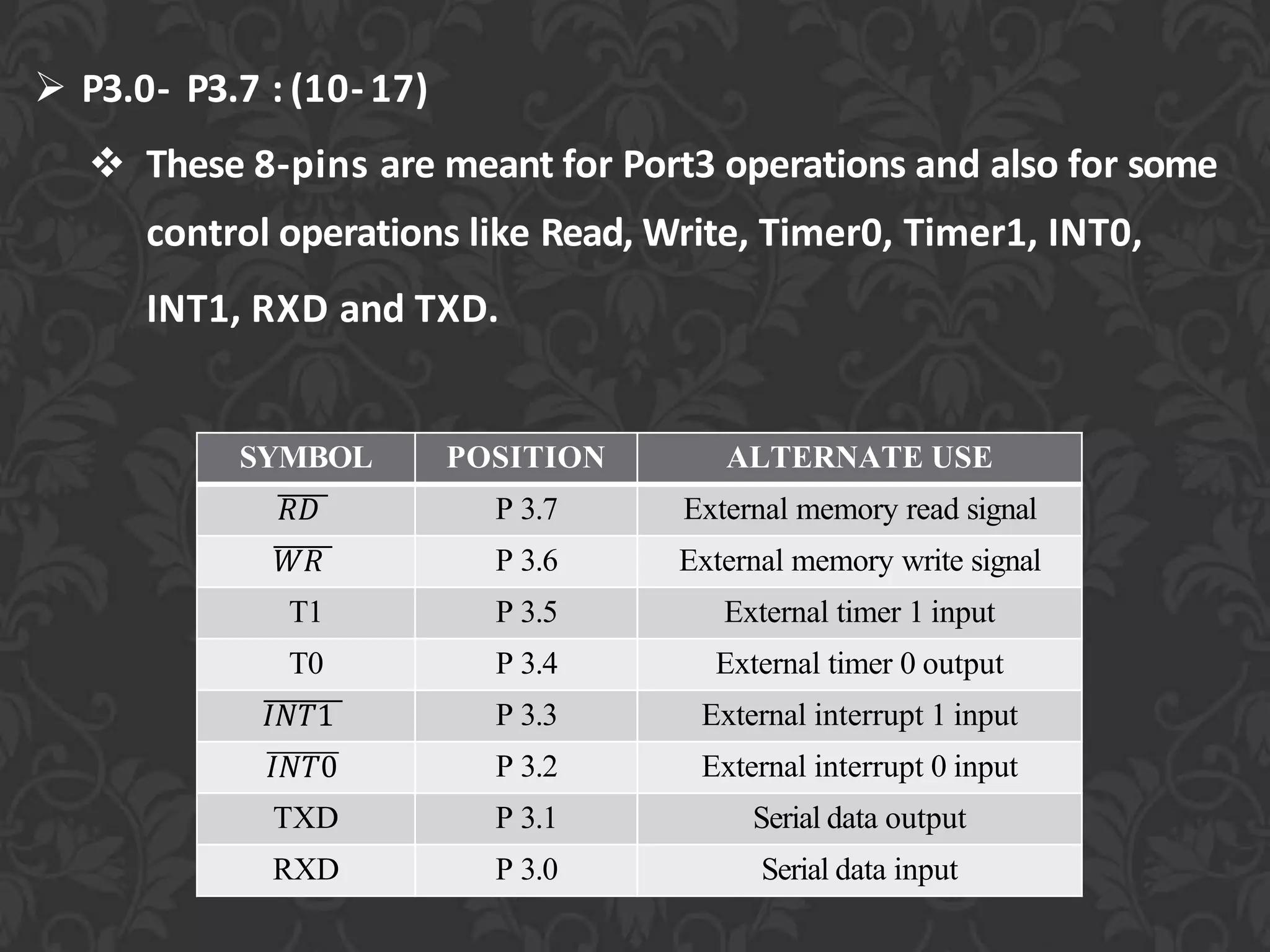
 P3.0- P3.7 : (10- 17)
 These 8-pins are meant for Port3 operations and also for some
control operations like Read, Write, Timer0, Timer1, INT0,
INT1, RXD and TXD.
SYMBOL POSITION ALTERNATE USE
𝑅𝐷 P 3.7 External memory read signal
𝑊𝑅 P 3.6 External memory write signal
T1 P 3.5 External timer 1 input
T0 P 3.4 External timer 0 output
𝐼𝑁𝑇1 P 3.3 External interrupt 1 input
𝐼𝑁𝑇0 P 3.2 External interrupt 0 input
TXD P 3.1 Serial data output
RXD P 3.0 Serial data input
 Pin 40 & pin 20
 Pin 40 = Vcc = +5v
 Pin 20 = Vss = GND
 XTAL1(Pin 19), XTAL2(Pin 18)
 These two pins are connected to Quartz crystal oscillator
which runs the on-chip oscillator.
 For generating an internal clock signal, the external
oscillator is connected at these two pins.
 If we use a source other than the crystal oscillator, it will be
connected to XTAL1 and XTAL2 is left unconnected.
 ALE – pin 30(Address Latch Enable)
 This is an output pin, which is active high.
 When connected to external memory , port 0 provides both
address and data i.e address and data are multiplexed
through port 0 .
 This ALE pin will demultiplex the address and data bus
.When the pin is High , the AD bus will act as address bus
otherwise the AD bus will act as Data bus.
 RST – pin 9(RESET)
 The RESET pin is an input pin and it is an active high pin.
 When a high pulse is applied to this pin the microcontroller will reset
and terminate all activities.
 It held high at least for two machine cycles, while oscillator is running
 PSEN– pin 29(Program Store Enable) :
 This is an output pin which is active low.
 When the microcontroller is accessing the program code stored in the
external ROM, this pin is connected tothe OE (Output Enable) pin of the
ROM.
 It is activated every six oscillator periods while reading external memory
 𝑬𝑨 – pin 31 (External Access):
 This pin is an active low pin.
 This pin is connected toground when microcontroller is
accessing the program code stored in the external memory
and connected to Vcc when it is accessing the program
code in the on chip memory.
 This pin should not be left Unconnected.
8051 pin description

8051 pin description

  • 2.
     The 8051is a 40 pin device, but out of these 40 pins, 32 are used for I/O  Many pins of 8051 are used for more than one function.  32 I/O pins = 4 eight bit ports = P0, P1, P2 and P3  All ports are bidirectional  Each ports consist of latch, an output driver and an input buffer.
  • 3.
     40 pinDIP  +5 volts DC.  Among the 40 pins , 32 pins = four parallel ports P0, P1, P2 and P3 . Remaining pins are VCC, GND, XTAL1, XTAL2, RST, EA , PSEN, ALE.  P0.0- P0.7(AD0-AD7) (32-39)  The port 0 pins multiplexed with (low order byte) Address/data pins .  If the microcontroller is accessing external memory, these pins will act as address/data pins otherwise, they are used for Port 0 pins.
  • 4.
     P1.0- P1.7(1 – 8)  These 8-pins are dedicated for Port 1 to perform input or output port operations.  P2.0- P2.7(A8-A15) (21-28)  The port 2 pins are multiplexed with the higher order address pins .  When the microcontroller is accessing external memory these pins provide the higher order address byte otherwise they act as Port 2 pins.
  • 5.
     P3.0- P3.7: (10- 17)  These 8-pins are meant for Port3 operations and also for some control operations like Read, Write, Timer0, Timer1, INT0, INT1, RXD and TXD. SYMBOL POSITION ALTERNATE USE 𝑅𝐷 P 3.7 External memory read signal 𝑊𝑅 P 3.6 External memory write signal T1 P 3.5 External timer 1 input T0 P 3.4 External timer 0 output 𝐼𝑁𝑇1 P 3.3 External interrupt 1 input 𝐼𝑁𝑇0 P 3.2 External interrupt 0 input TXD P 3.1 Serial data output RXD P 3.0 Serial data input
  • 6.
     Pin 40& pin 20  Pin 40 = Vcc = +5v  Pin 20 = Vss = GND  XTAL1(Pin 19), XTAL2(Pin 18)  These two pins are connected to Quartz crystal oscillator which runs the on-chip oscillator.  For generating an internal clock signal, the external oscillator is connected at these two pins.  If we use a source other than the crystal oscillator, it will be connected to XTAL1 and XTAL2 is left unconnected.
  • 7.
     ALE –pin 30(Address Latch Enable)  This is an output pin, which is active high.  When connected to external memory , port 0 provides both address and data i.e address and data are multiplexed through port 0 .  This ALE pin will demultiplex the address and data bus .When the pin is High , the AD bus will act as address bus otherwise the AD bus will act as Data bus.
  • 8.
     RST –pin 9(RESET)  The RESET pin is an input pin and it is an active high pin.  When a high pulse is applied to this pin the microcontroller will reset and terminate all activities.  It held high at least for two machine cycles, while oscillator is running  PSEN– pin 29(Program Store Enable) :  This is an output pin which is active low.  When the microcontroller is accessing the program code stored in the external ROM, this pin is connected tothe OE (Output Enable) pin of the ROM.  It is activated every six oscillator periods while reading external memory
  • 9.
     𝑬𝑨 –pin 31 (External Access):  This pin is an active low pin.  This pin is connected toground when microcontroller is accessing the program code stored in the external memory and connected to Vcc when it is accessing the program code in the on chip memory.  This pin should not be left Unconnected.