Piezo Resistive Pressure Sensor
&
Case Study of MAP Sensor
By
Pratyusha
And
A.Jenifer Sofia
Contents
Pressure Sensing
Piezo resistance
Case Study-Motorola MAP Sensor
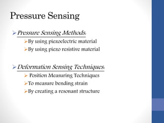
Pressure Sensing
Pressure Sensing Methods:
By using piezoelectric material
By using piezo resistive material
Deformation Sensing Techniques:
 Position Measuring Techniques
To measure bending strain
By creating a resonant structure
Piezoresistivity
 Change in electrical resistivity when
mechanical stress is applied
Affects metals as well as semiconductors
Analytic Formulation in Cubic
Materials
 The relationship between electric field and
current density is given by 𝜀 = 𝜌ℯ + π. 𝜎 . 𝒥
Where
𝜌ℯ is the resistivity tensor of second rank
𝜋 is the fourth rank piezo resistive tensor
𝜎 is the full second-rank stress tensor, and
𝒥 is the current density.
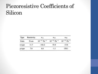
Piezoresistive Coefficients of
Silicon
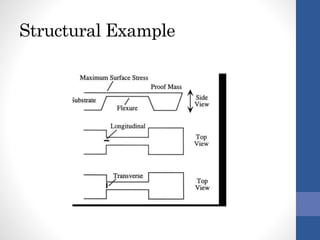
Structural Example
MOTOROLA MAP SENSOR
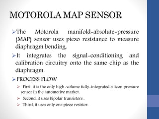
The Motorola manifold-absolute-pressure
(MAP) sensor uses piezo resistance to measure
diaphragm bending.
It integrates the signal-conditioning and
calibration circuitry onto the same chip as the
diaphragm.
PROCESS FLOW
 First, it is the only high-volume fully-integrated silicon pressure
sensor in the automotive market.
 Second, it uses bipolar transistors .
 Third, it uses only one piezo resistor.
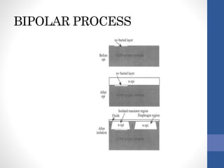
BIPOLAR PROCESS
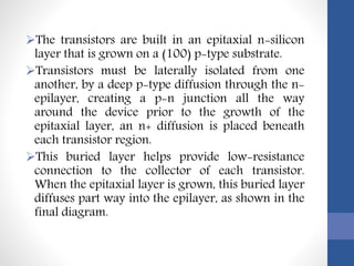
The transistors are built in an epitaxial n-silicon
layer that is grown on a (100) p-type substrate.
Transistors must be laterally isolated from one
another, by a deep p-type diffusion through the n-
epilayer, creating a p-n junction all the way
around the device prior to the growth of the
epitaxial layer, an n+ diffusion is placed beneath
each transistor region.
This buried layer helps provide low-resistance
connection to the collector of each transistor.
When the epitaxial layer is grown, this buried layer
diffuses part way into the epilayer, as shown in the
final diagram.
DETAILS OF DIAPHRAGM
AND PEIZORESISTOR
Diaphragm dimensions are 1000 × 1000 um
square, with a thickness of 20 um
Piezo resistor is located near the edge center,
where stress is highest, oriented at a 45 angle to the
side of the square diaphragm
The p-type piezo resistor has four contacts two-
current along the resistor axis and two - transverse
voltage taps which are connected to a impedance
op-amp input.
The other two are transverse voltage taps which
are connected to a high-impedance op-amp input
so as to draw no current
MOTOROLA XDUCER
PEIZORESISTOR
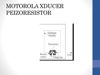
The dark-shaded contact regions are much
wider than the piezoresistor and are doped p+;
hence these regions have lower resistance than
the piezoresistor itself.
Diaphragm edge is along a [110] direction in a
(100) plane, it means that the resistor axis is
actually along a [100] direction.
We select an axis system in which the “1” axis
is along the resistor length, the “2” axis is in the
plane of the diaphragm, and the “3” axis is
normal to the diaphragm
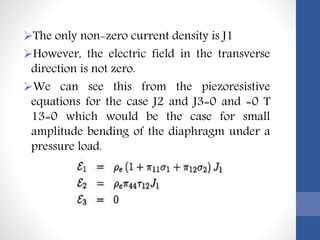
The only non-zero current density is J1
However, the electric field in the transverse
direction is not zero.
We can see this from the piezoresistive
equations for the case J2 and J3=0 and =0 T
13=0 which would be the case for small
amplitude bending of the diaphragm under a
pressure load.
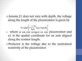
Assume J1 does not vary with depth, the voltage
along the length of the piezoresistor is given by
 where is LR the length of the piezoresistor and
x1 is the spatial coordinate for an axis aligned
along the resistor length.
Prefactor is the voltage due to the unstrained
resistivity of the piezoresistor.
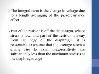
The integral term is the change in voltage due
to a length averaging of the piezoresistance
effect
Part of the resistor is off the diaphragm, where
stress is low, and part of the resistor is away
from the edge of the diaphragm, it is
reasonable to assume that the average stresses
giving rise to axial piezoresistivity are
substantially less than the maximum stresses at
the diaphragm edge
STRESS ANALYSIS
An approximate model for the bending of a plate
under the effects of a pressure load is given by
The energy-method analysis with this trial
function led to a load-deflection equation of the
form
 For the present analysis,it is zero because the
diaphragm is bulk micromachined.
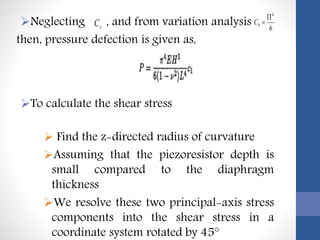
Neglecting , and from variation analysis
then, pressure defection is given as,
To calculate the shear stress
 Find the z-directed radius of curvature
Assuming that the piezoresistor depth is
small compared to the diaphragm
thickness
We resolve these two principal-axis stress
components into the shear stress in a
coordinate system rotated by 45°
sC 6
4

bC
SIGNAL-CONDITIONING AND
CALIBRATION
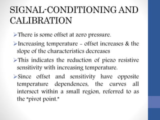
There is some offset at zero pressure.
Increasing temperature - offset increases & the
slope of the characteristics decreases
This indicates the reduction of piezo resistive
sensitivity with increasing temperature.
Since offset and sensitivity have opposite
temperature dependences, the curves all
intersect within a small region, referred to as
the “pivot point.”
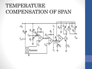
TEMPERATURE
COMPENSATION OF SPAN
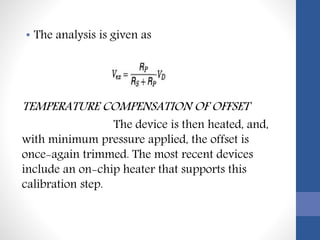
• The analysis is given as
TEMPERATURE COMPENSATION OF OFFSET
The device is then heated, and,
with minimum pressure applied, the offset is
once-again trimmed. The most recent devices
include an on-chip heater that supports this
calibration step.
DEVICE NOISE
System noise comes from several source
- noise in the piezo resistors
- front-end amplifier noise, presumed to
have both a white and 1/f component.
RECENT DESIGN CHANGES
Thus, an improvement in control of one
dimension allows a dramatic reduction in chip size,
from 3.05 mm square to 2.76 mm square, a 22%
area reduction.
HIGHER-ORDER EFFECTS
 The longitudinal piezoresistance,
 Detailed modeling of the stress distribution in
the diaphragm
 Nonlinearities in the temperature coefficient
of resistance
 Issues of resistor placement and stress
averaging
Piezo Resistive Pressure Sensor & Case Study of MAP Sensor

Piezo Resistive Pressure Sensor & Case Study of MAP Sensor

  • 1.
    Piezo Resistive PressureSensor & Case Study of MAP Sensor By Pratyusha And A.Jenifer Sofia
  • 2.
  • 3.
    Pressure Sensing Pressure SensingMethods: By using piezoelectric material By using piezo resistive material Deformation Sensing Techniques:  Position Measuring Techniques To measure bending strain By creating a resonant structure
  • 4.
    Piezoresistivity  Change inelectrical resistivity when mechanical stress is applied Affects metals as well as semiconductors
  • 5.
    Analytic Formulation inCubic Materials  The relationship between electric field and current density is given by 𝜀 = 𝜌ℯ + π. 𝜎 . 𝒥 Where 𝜌ℯ is the resistivity tensor of second rank 𝜋 is the fourth rank piezo resistive tensor 𝜎 is the full second-rank stress tensor, and 𝒥 is the current density.
  • 6.
  • 7.
  • 9.
    MOTOROLA MAP SENSOR TheMotorola manifold-absolute-pressure (MAP) sensor uses piezo resistance to measure diaphragm bending. It integrates the signal-conditioning and calibration circuitry onto the same chip as the diaphragm. PROCESS FLOW  First, it is the only high-volume fully-integrated silicon pressure sensor in the automotive market.  Second, it uses bipolar transistors .  Third, it uses only one piezo resistor.
  • 10.
  • 11.
    The transistors arebuilt in an epitaxial n-silicon layer that is grown on a (100) p-type substrate. Transistors must be laterally isolated from one another, by a deep p-type diffusion through the n- epilayer, creating a p-n junction all the way around the device prior to the growth of the epitaxial layer, an n+ diffusion is placed beneath each transistor region. This buried layer helps provide low-resistance connection to the collector of each transistor. When the epitaxial layer is grown, this buried layer diffuses part way into the epilayer, as shown in the final diagram.
  • 12.
    DETAILS OF DIAPHRAGM ANDPEIZORESISTOR Diaphragm dimensions are 1000 × 1000 um square, with a thickness of 20 um Piezo resistor is located near the edge center, where stress is highest, oriented at a 45 angle to the side of the square diaphragm The p-type piezo resistor has four contacts two- current along the resistor axis and two - transverse voltage taps which are connected to a impedance op-amp input. The other two are transverse voltage taps which are connected to a high-impedance op-amp input so as to draw no current
  • 13.
  • 14.
    The dark-shaded contactregions are much wider than the piezoresistor and are doped p+; hence these regions have lower resistance than the piezoresistor itself. Diaphragm edge is along a [110] direction in a (100) plane, it means that the resistor axis is actually along a [100] direction. We select an axis system in which the “1” axis is along the resistor length, the “2” axis is in the plane of the diaphragm, and the “3” axis is normal to the diaphragm
  • 15.
    The only non-zerocurrent density is J1 However, the electric field in the transverse direction is not zero. We can see this from the piezoresistive equations for the case J2 and J3=0 and =0 T 13=0 which would be the case for small amplitude bending of the diaphragm under a pressure load.
  • 16.
    Assume J1 doesnot vary with depth, the voltage along the length of the piezoresistor is given by  where is LR the length of the piezoresistor and x1 is the spatial coordinate for an axis aligned along the resistor length. Prefactor is the voltage due to the unstrained resistivity of the piezoresistor.
  • 17.
    The integral termis the change in voltage due to a length averaging of the piezoresistance effect Part of the resistor is off the diaphragm, where stress is low, and part of the resistor is away from the edge of the diaphragm, it is reasonable to assume that the average stresses giving rise to axial piezoresistivity are substantially less than the maximum stresses at the diaphragm edge
  • 18.
    STRESS ANALYSIS An approximatemodel for the bending of a plate under the effects of a pressure load is given by The energy-method analysis with this trial function led to a load-deflection equation of the form  For the present analysis,it is zero because the diaphragm is bulk micromachined.
  • 19.
    Neglecting , andfrom variation analysis then, pressure defection is given as, To calculate the shear stress  Find the z-directed radius of curvature Assuming that the piezoresistor depth is small compared to the diaphragm thickness We resolve these two principal-axis stress components into the shear stress in a coordinate system rotated by 45° sC 6 4  bC
  • 20.
    SIGNAL-CONDITIONING AND CALIBRATION There issome offset at zero pressure. Increasing temperature - offset increases & the slope of the characteristics decreases This indicates the reduction of piezo resistive sensitivity with increasing temperature. Since offset and sensitivity have opposite temperature dependences, the curves all intersect within a small region, referred to as the “pivot point.”
  • 21.
  • 22.
    • The analysisis given as TEMPERATURE COMPENSATION OF OFFSET The device is then heated, and, with minimum pressure applied, the offset is once-again trimmed. The most recent devices include an on-chip heater that supports this calibration step.
  • 23.
    DEVICE NOISE System noisecomes from several source - noise in the piezo resistors - front-end amplifier noise, presumed to have both a white and 1/f component. RECENT DESIGN CHANGES Thus, an improvement in control of one dimension allows a dramatic reduction in chip size, from 3.05 mm square to 2.76 mm square, a 22% area reduction.
  • 24.
    HIGHER-ORDER EFFECTS  Thelongitudinal piezoresistance,  Detailed modeling of the stress distribution in the diaphragm  Nonlinearities in the temperature coefficient of resistance  Issues of resistor placement and stress averaging

Editor's Notes

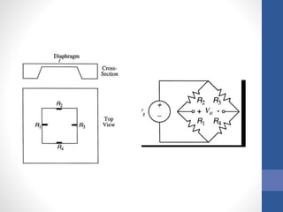
  • #4 Piezoelectric material: transduce normal stress to voltage. The other most frequently used method is: one could apply the pressure to one side of a deformable diaphragm, a reference pressure to the other side, and determine how much the diaphragm deforms. The sensing material in a piezoresistive pressure sensor is a diaphragm formed on a silicon substrate, which bends with applied pressure. A deformation occurs in the crystal lattice of the diaphragm because of that bending. This deformation causes a change in the band structure of the piezoresistors that are placed on the diaphragm, leading to a change in the resistivity of the material. This change can be an increase or a decrease according to the orientation of the resistors. capacitance change, some optical signature, or even the change in current in a tunneling tip are examples of position measuring tech.
  • #5 crystalline materials like Silicon, is principally a change in the electronic structure which leads to a modification of the charge carriers’ effective mass. With help of strain gauges metals can be measured.
  • #7 These coefficients depend strongly on the doping type. An important fact is that at higher doping, the temperature dependence of the piezoresistive coefficients becomes small.
  • #8 For example..if we r using p type resistor, first we have to ingrain it on a n type susbstrate to achieve junction isolation & vice versa. The tensor coeff.of longitudinal & transverse type are same in mag but opp in nature. Polycrystalline are solids composed of many crystallites of varying size & orientation. Since the transverse resistor is placed at the exact position….it experiences largest response,when placed at right point..it has max bending stress whereas for longi not every part of resistor experiences stress coz it extends over the length. If we want a sensitive device then transverse orientation can be preferred & if we want a less costly device & less robust compensation technique then longi can be used. All these features & design calibrations can be seen in case study of MAP.
  • #9 110 direction. R1 & r3 have longi stress & r2 & r4 have transverse stress. Since they r placed on a plate…if r1 has longi stress then it must also have transverse stress.