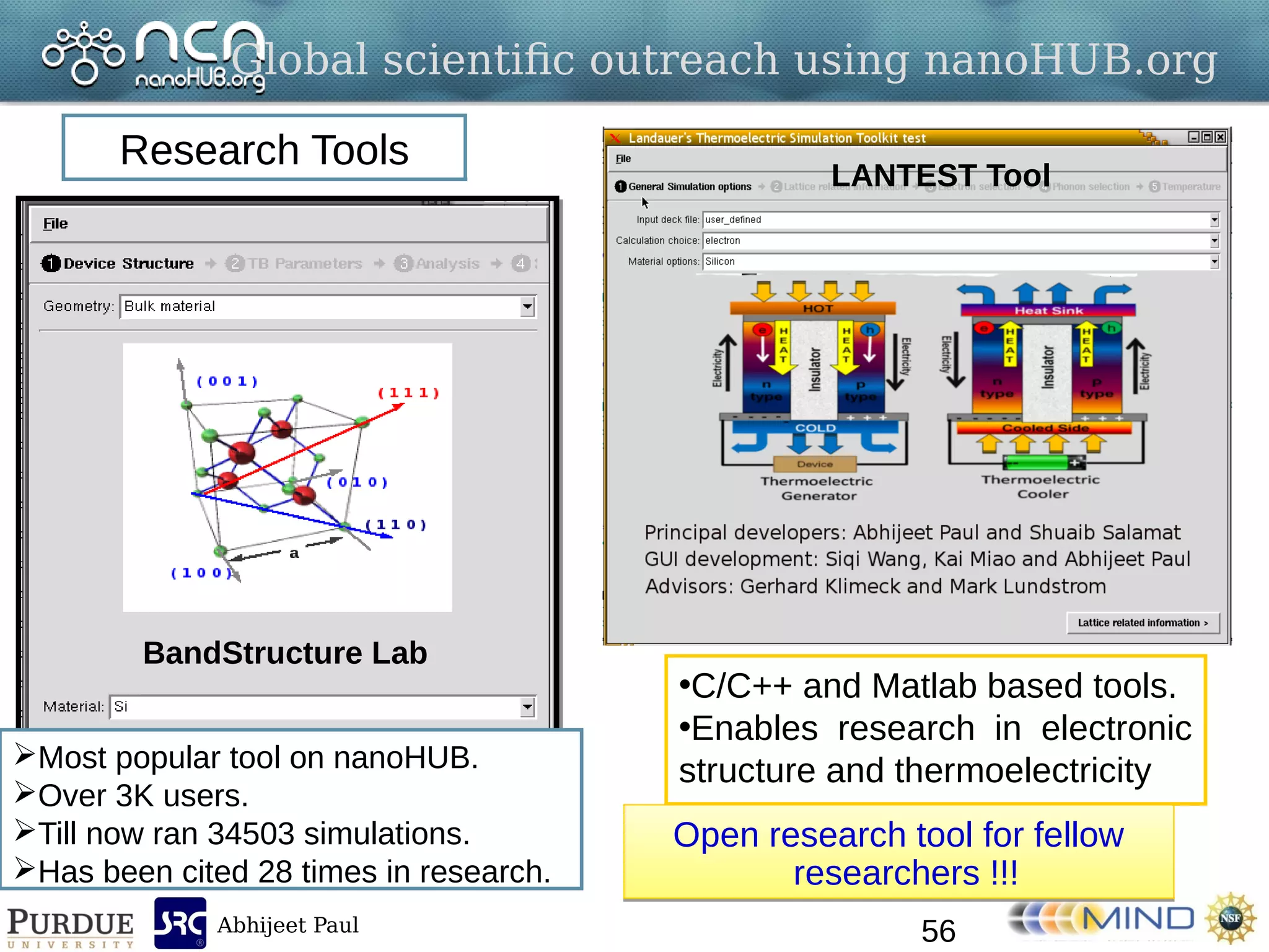
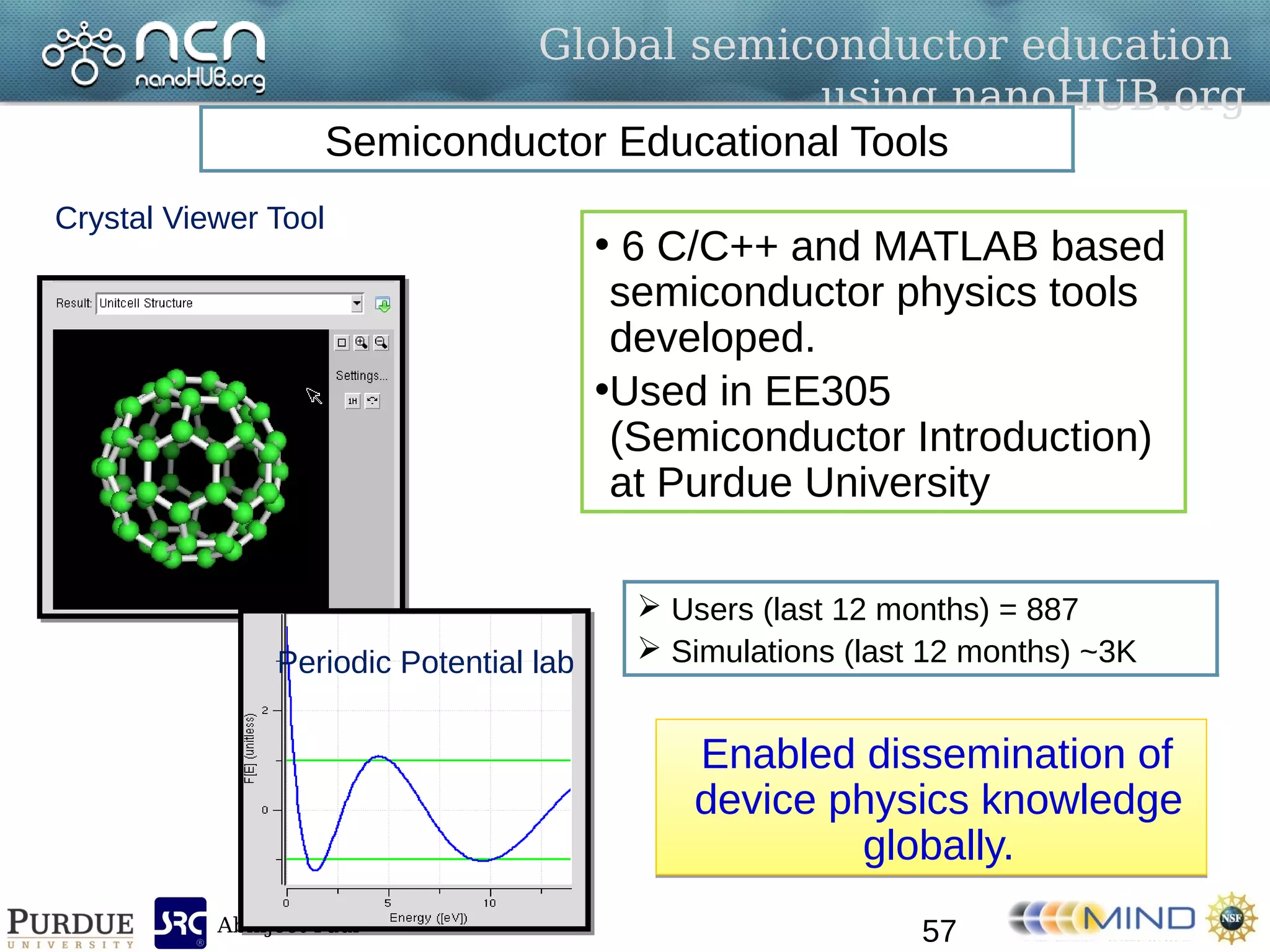
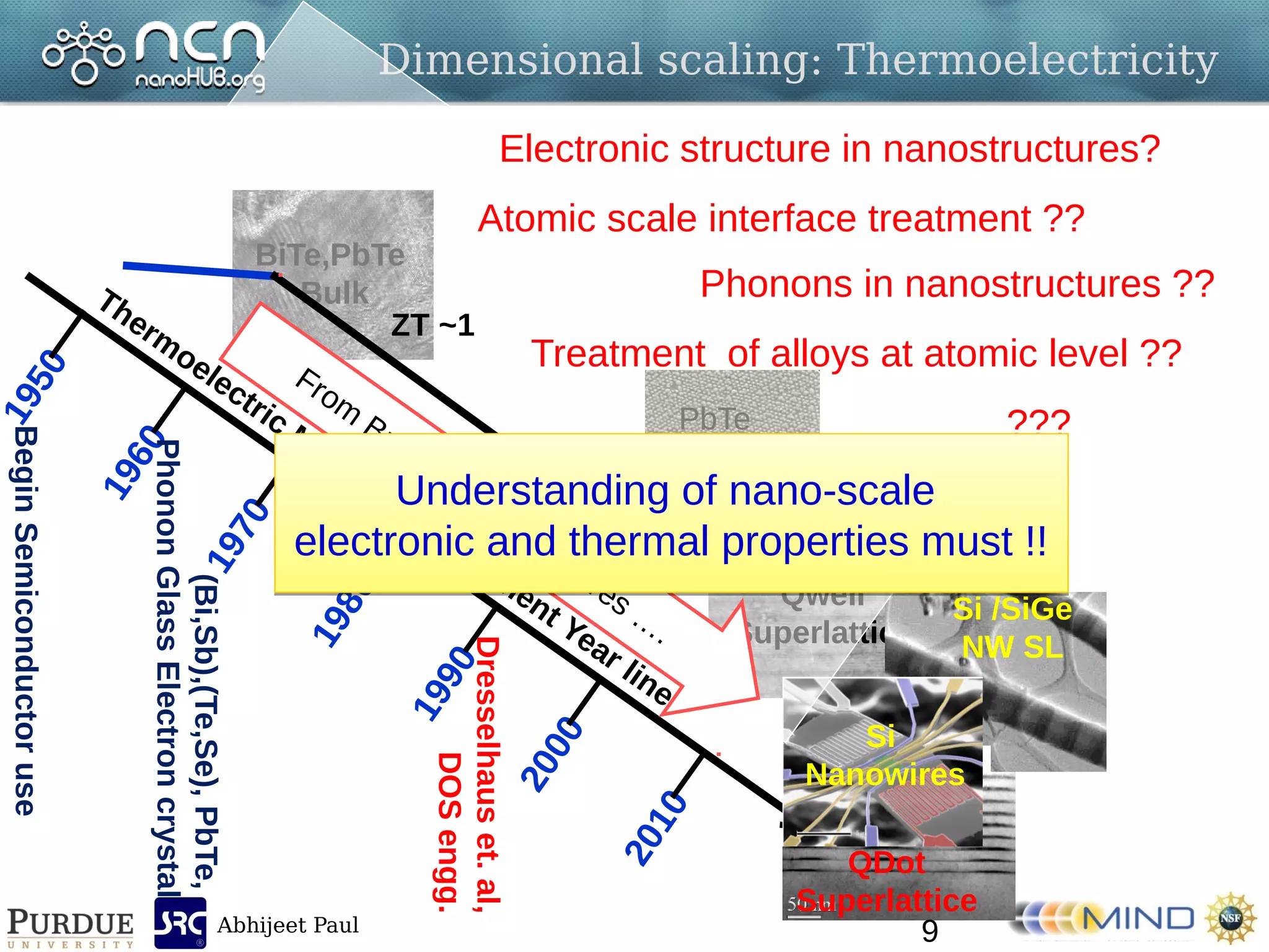
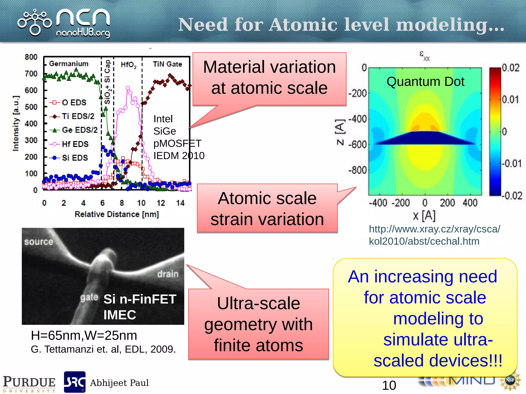
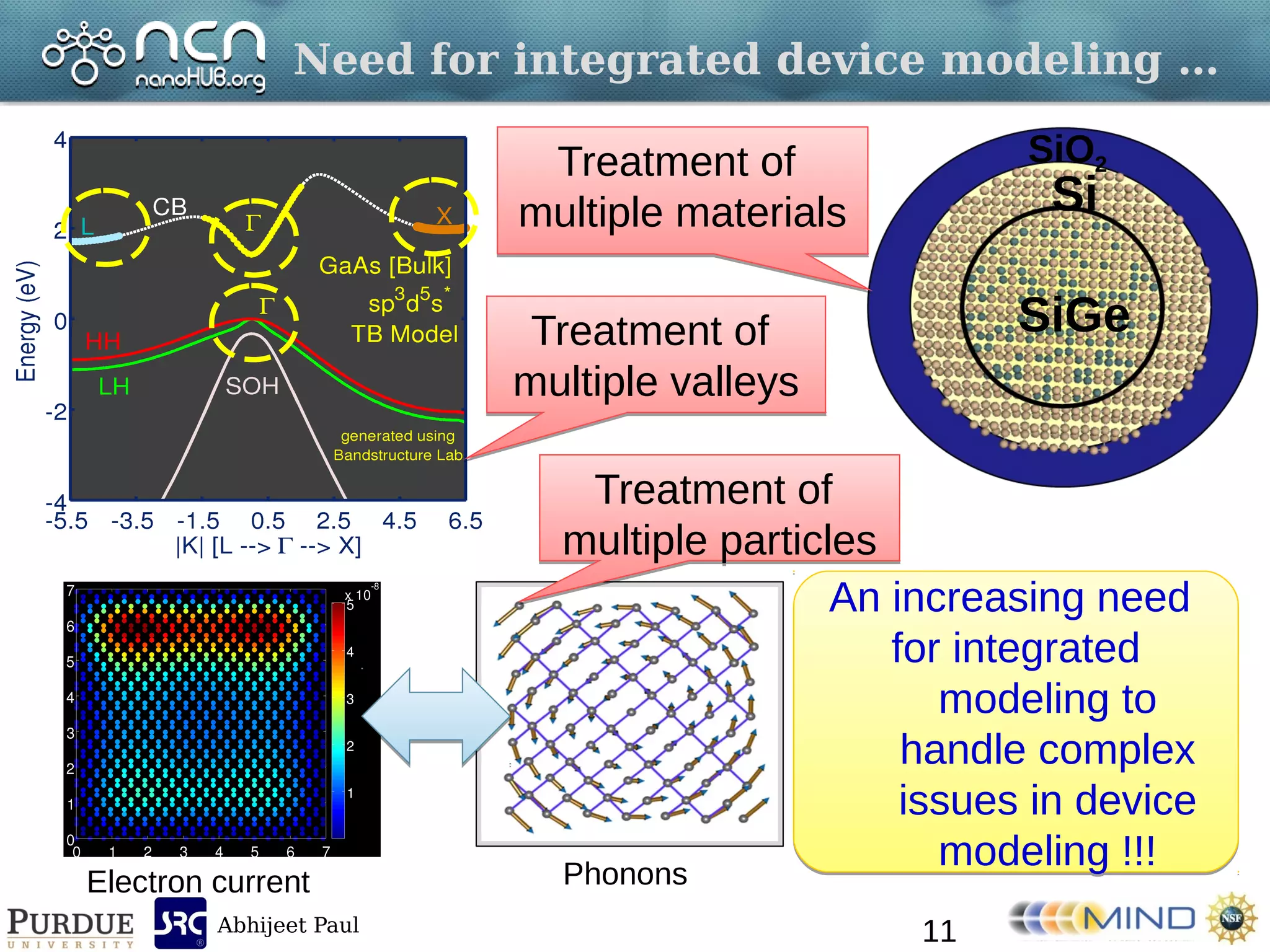
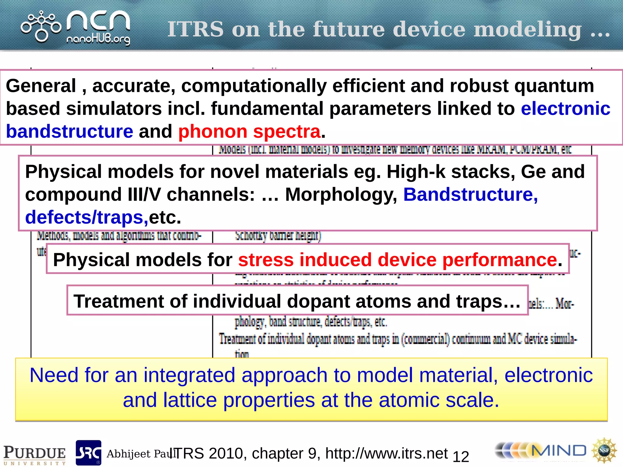
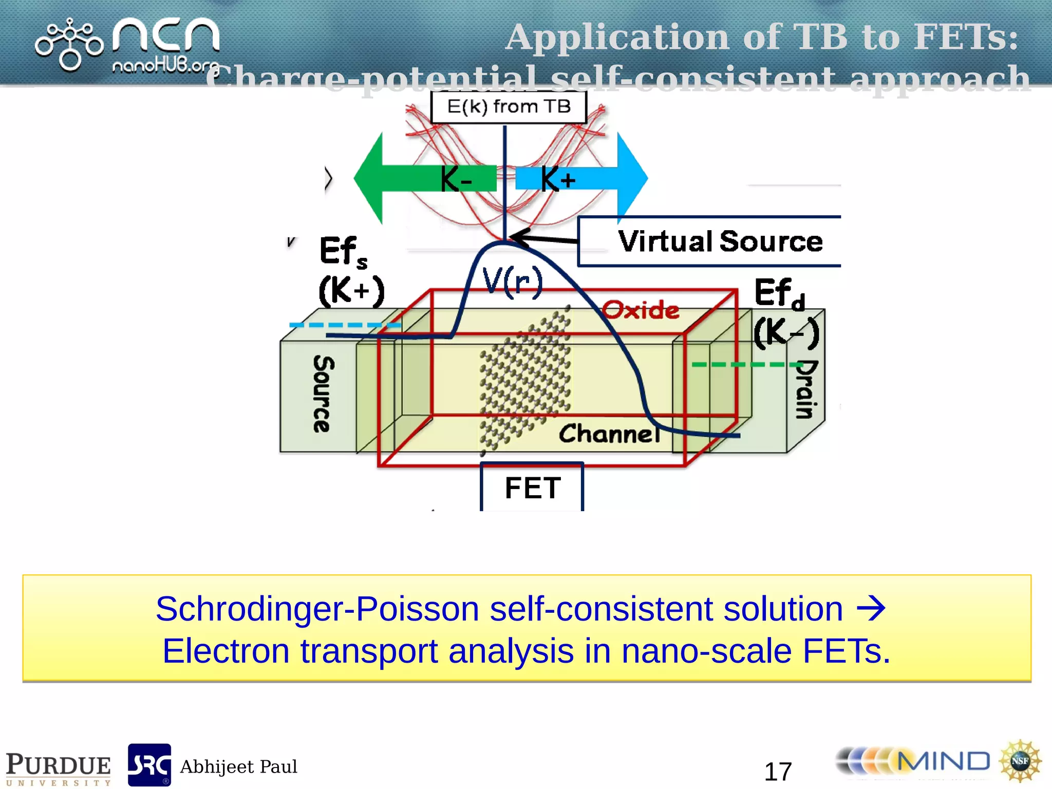
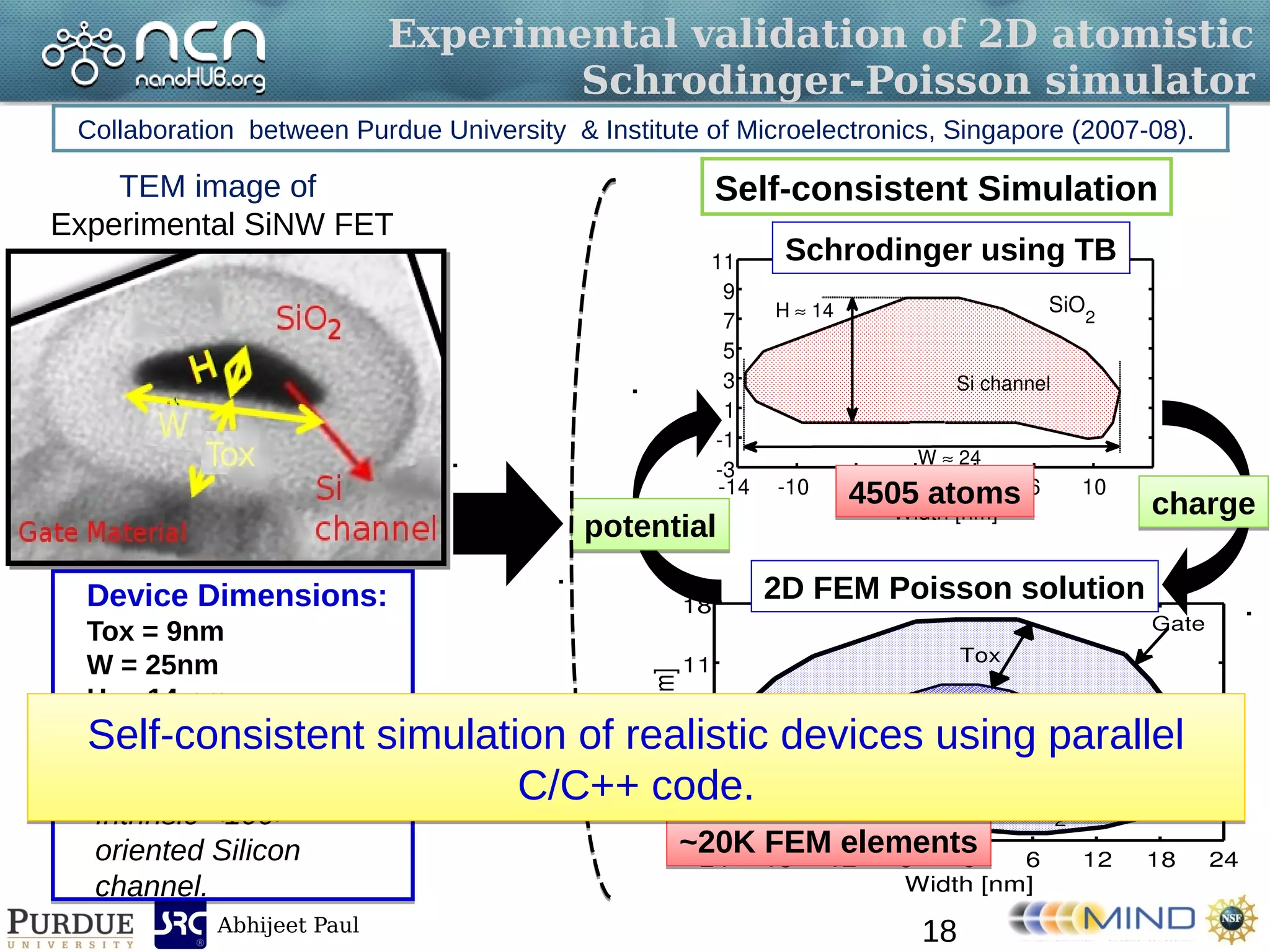
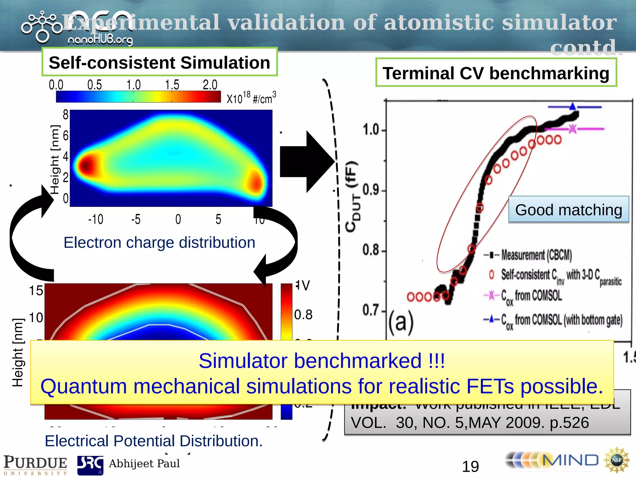
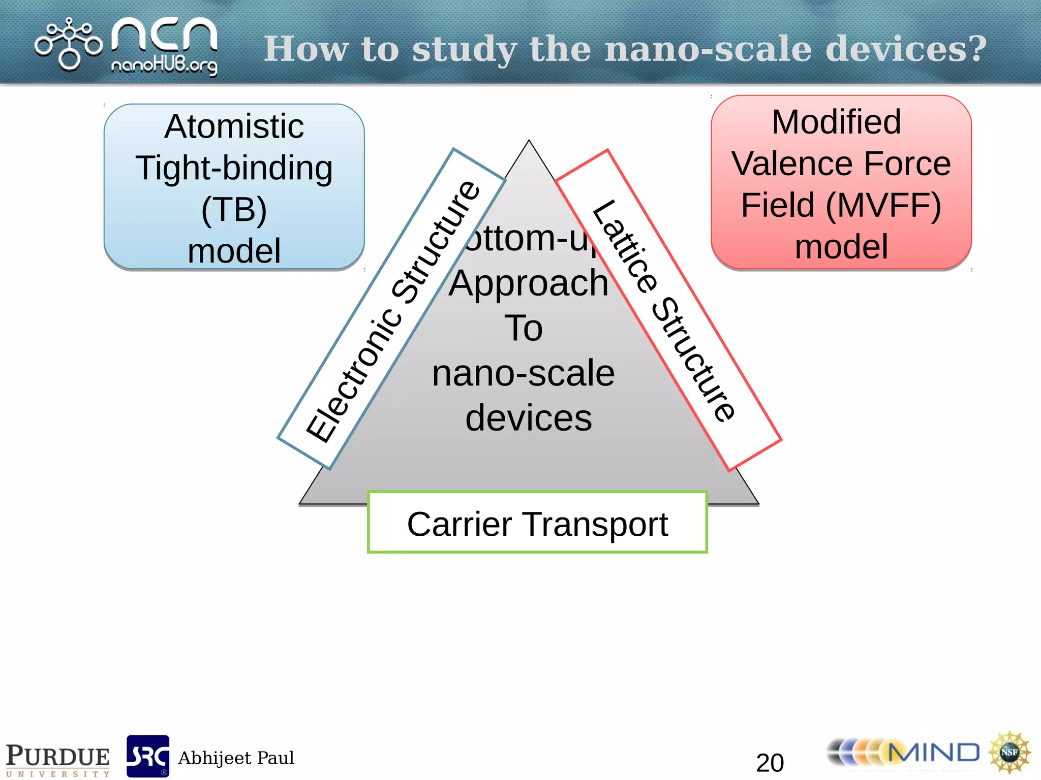
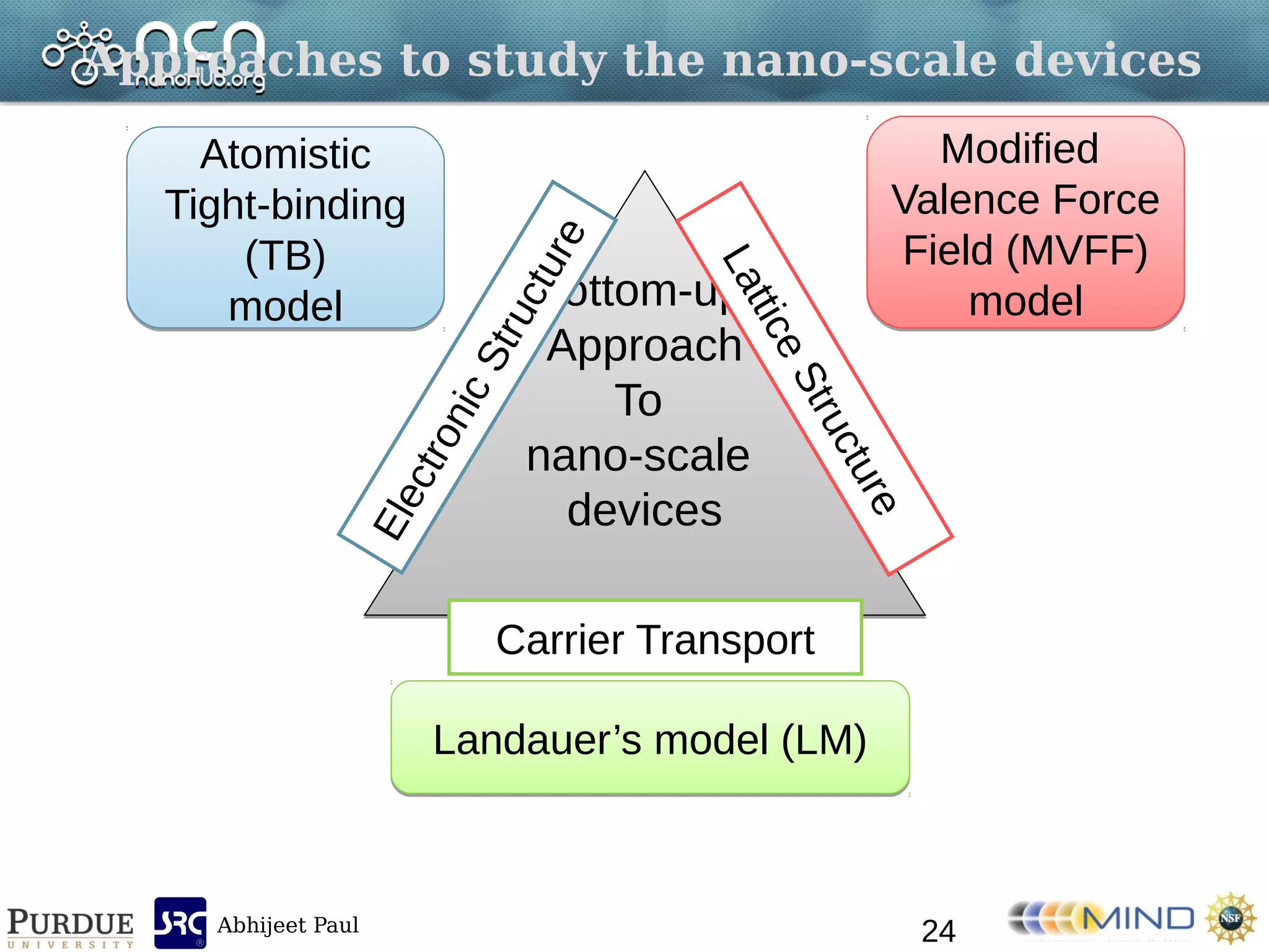
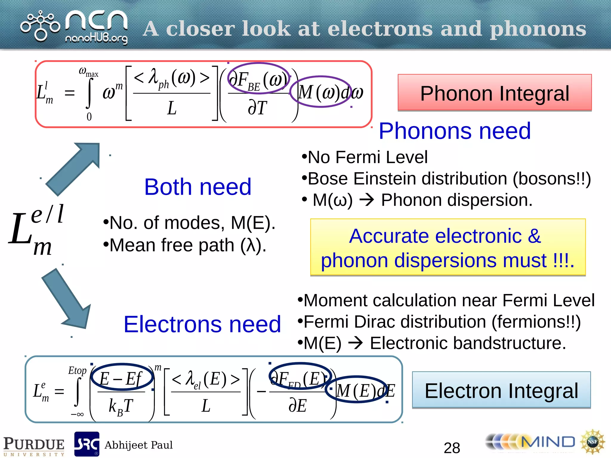
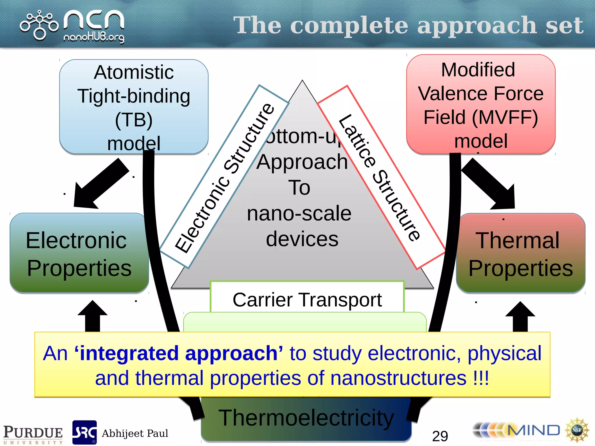
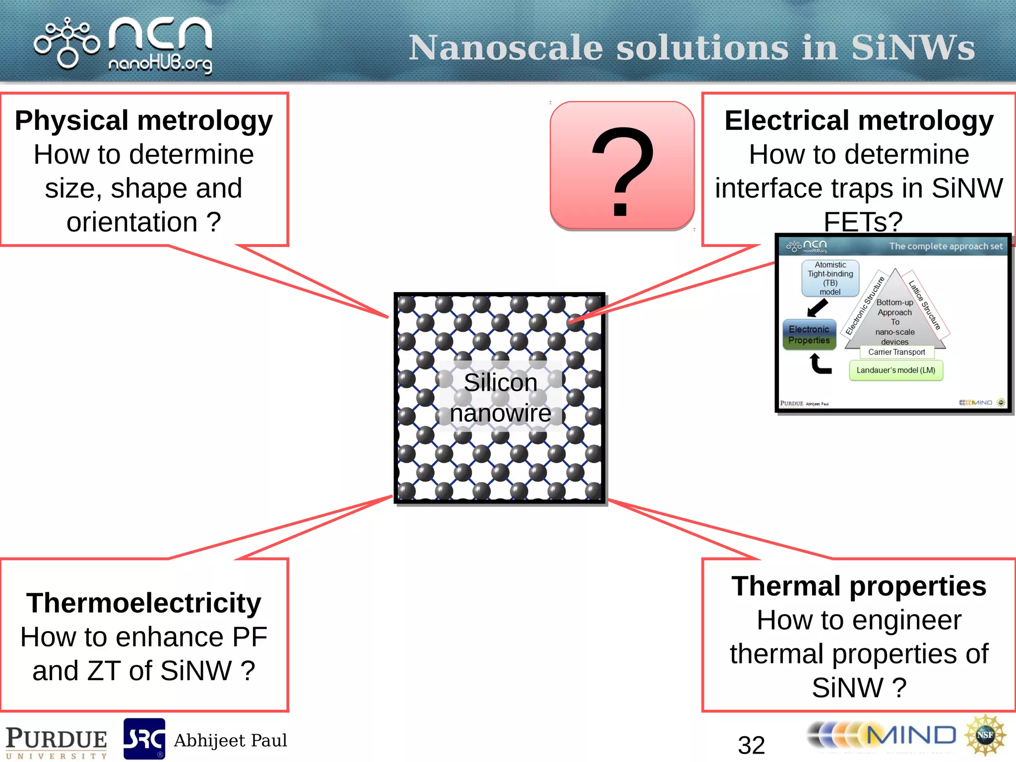
This document provides an outline for a talk on electronic and thermal properties of semiconductor nanostructures from atomistic modeling and simulation. It motivates the importance of integrated atomistic simulation to study next-generation devices facing CMOS scaling challenges. It describes using an atomistic tight-binding approach and charge-potential self-consistent solution to model silicon nanowire field effect transistors, validated against experimental devices. The talk aims to discuss applications to silicon and gallium arsenide nanostructures and disseminating findings through nanohub.org.
![Abhijeet Paul
PhD timeline and progress
[A] N. Singh et. al, EDL 2006 [B] A. Hochbaum et. al, Nature, 2008
[C] Yu et. al, Nature, 2010. [D] Pernot et. al, Nature, 2010.
Important experimental works that guided this PhD work.Important experimental works that guided this PhD work.
3](https://image.slidesharecdn.com/979da63d-ab42-44d9-a501-ce2e9d485a15-160110064319/75/PhD_10_2011_Abhijeet_Paul-3-2048.jpg)
![Abhijeet Paul
Phonon dispersion calculation:
Modified VFF (MVFF) model
Old Keating
Model [1]
[A]
Bond-stretching(α)
Δr
[B]
Bond-bending(β)
Δθ
[C] Cross-bond
stretch bend (γ)
[2] Zunger et. al. 1999Δθ
Δr
Imp. For polar materials [2]
Imp. for
polar
materials [2]
[F]
Coulomb
interaction
[E]
Δθ1
Δθ2
Coplanar bond
bending(τ)
Imp. for non-polar materials
([3] Sui et. al,
[D]
Δr1
Δr2
Cross bond
Stretching (δ)
Short
Range
Short
Range
[1] Keating. Phys. Rev. 145, 1966.
[2] PRB, 59,2881, 1999.
[3] PRB, 48, 17938,1993
Long
Range
Long
Range
21
New combination of Interactions:
Modified Valence Force Field
Calculate phonons in zinc-blende
materials.
New combination of Interactions:
Modified Valence Force Field
Calculate phonons in zinc-blende
materials.](https://image.slidesharecdn.com/979da63d-ab42-44d9-a501-ce2e9d485a15-160110064319/75/PhD_10_2011_Abhijeet_Paul-21-2048.jpg)
![Abhijeet Paul
Bulk Si
Expt. (dots) [1]
What is the need for a new phonon model??
Accurate phonon model crucial for correct calculation of
phonon dispersion in nanostructures.
Accurate phonon model crucial for correct calculation of
phonon dispersion in nanostructures.
Bulk Si
Expt. (dots) [1]
[1] Nelsin et. al, PRB, 6, 3777, 1972. 22
Keating VFF Model
Over estimates
acoustic modes
at zone edges.
Over estimates
optical modes
New MVFF model matchs the
dispersion very well in the entire
Brillouin zone !!!
Expt. Data[1], inelastic
neutron scattering
(80K and 300K).
Expt. Data[1], inelastic
neutron scattering
(80K and 300K).](https://image.slidesharecdn.com/979da63d-ab42-44d9-a501-ce2e9d485a15-160110064319/75/PhD_10_2011_Abhijeet_Paul-22-2048.jpg)
![Abhijeet Paul
1D periodic [100] Si
nanowire structure.
Surface atoms free to
vibrate.
1D periodic [100] Si
nanowire structure.
Surface atoms free to
vibrate.
[100] free
standing
SiNW
qx [norm.] X
Bulk Si
6 branches
Phonon dispersion in free-standing nanowires
23
Strong phonon confinement responsible for different lattice
properties in SiNWs compared to bulk.
Strong phonon confinement responsible for different lattice
properties in SiNWs compared to bulk.
Lot of flat bands (zero velocity)
resulting in phonon confinement.
2 branches
1 branch
1 branch
2 branches](https://image.slidesharecdn.com/979da63d-ab42-44d9-a501-ce2e9d485a15-160110064319/75/PhD_10_2011_Abhijeet_Paul-23-2048.jpg)
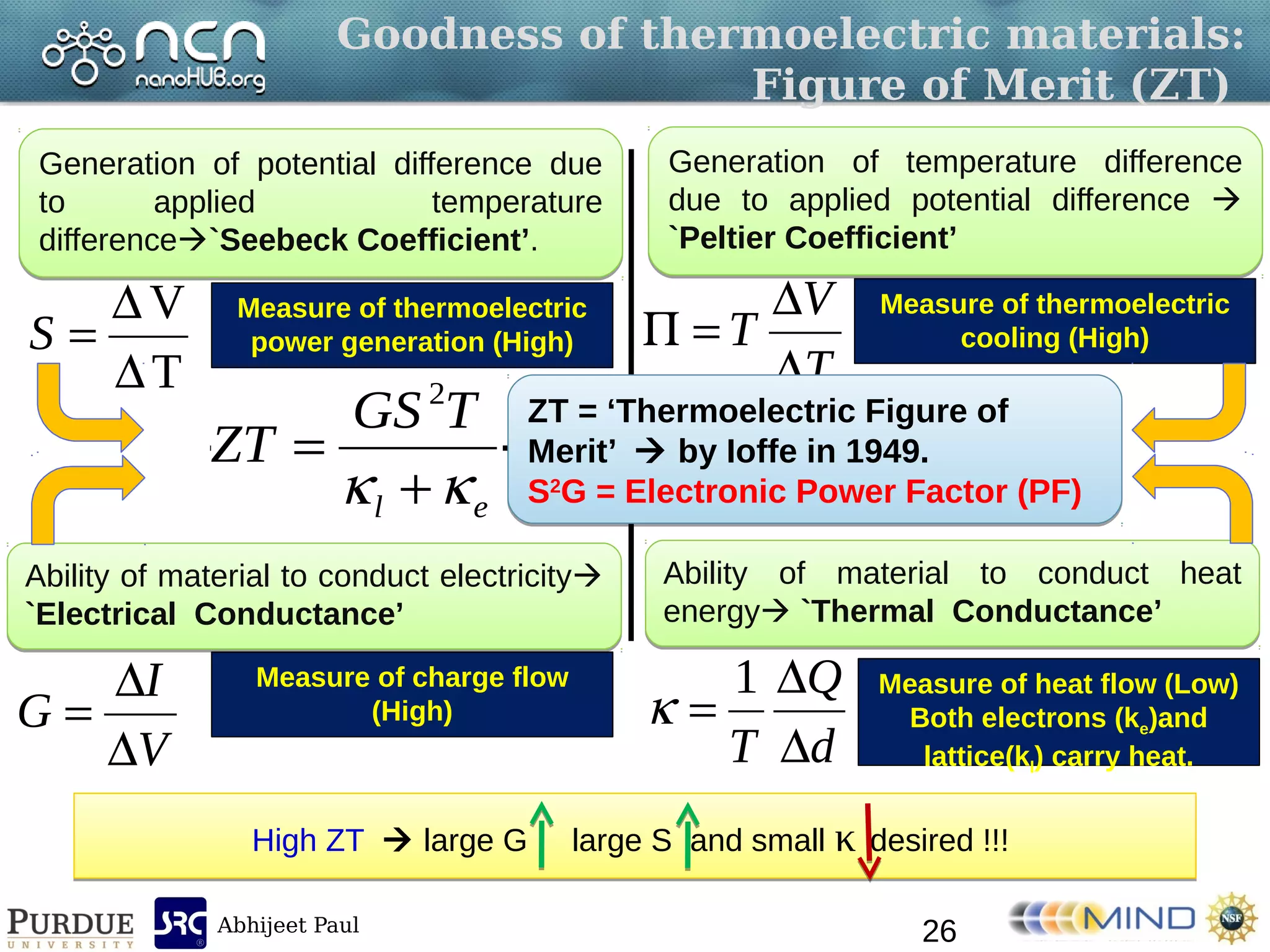
![Abhijeet Paul
Material A
Material B
How to analyze thermoelectric
properties of materials ?
V1
V2
IN
O
U
T
Tc Th
IQ
Ie
Ie
Steady-state linear thermoelectric (Onsager’s) relations [1,2]
[1] L. Onsager, Phys. Rev. 37 405 (1931).
[2] G. D. Mahan, Many-body Physics.
lehhch TTTTTTVVV ,2,,21
TT q
Tk
V B
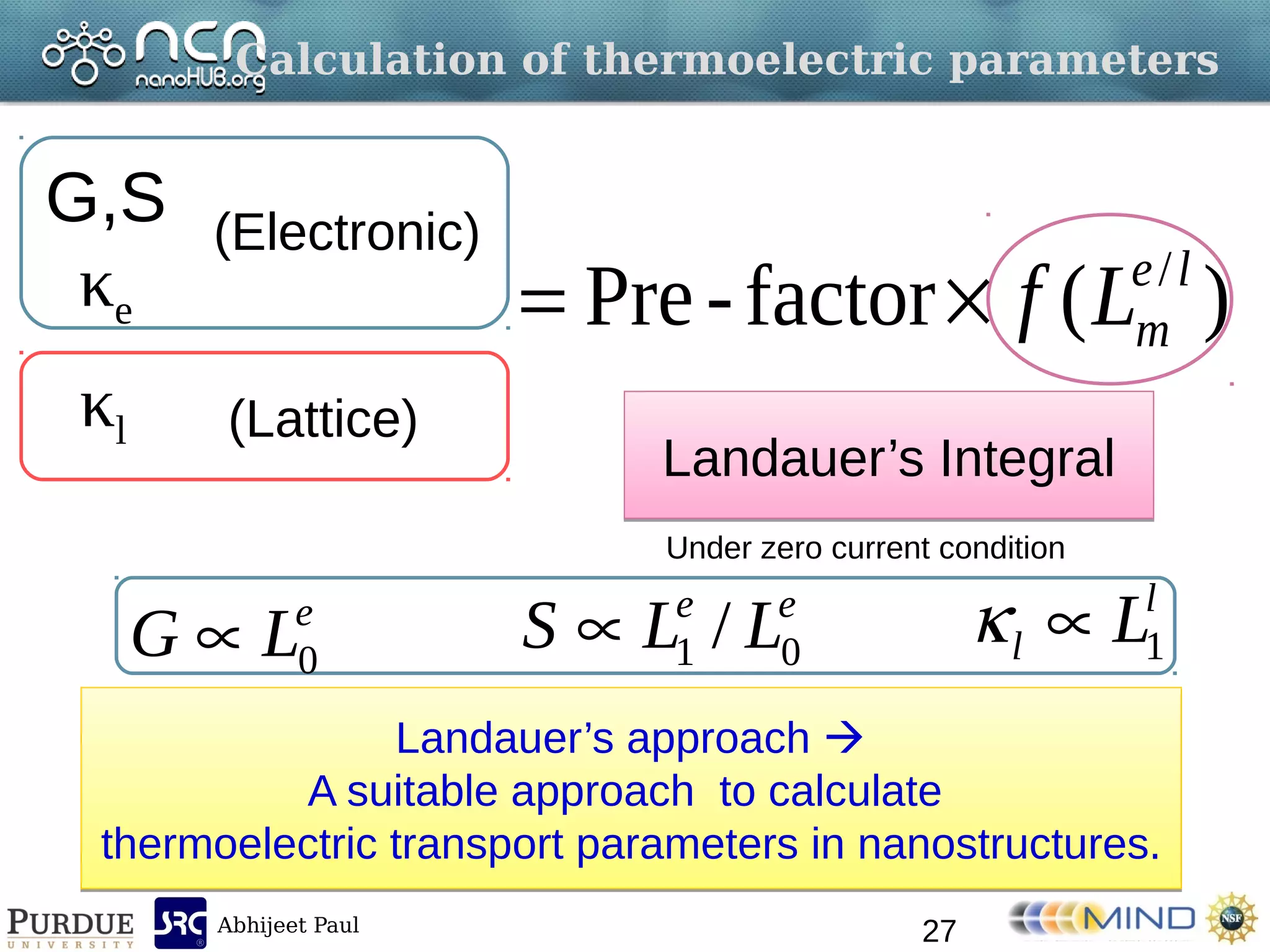
Landauer’s Formula can be used to
evaluate the transport parameters
Landauer’s Formula can be used to
evaluate the transport parameters
TTGSVTGSIQ .. 2
TGSVGIe ..
Electric current Heat current
25](https://image.slidesharecdn.com/979da63d-ab42-44d9-a501-ce2e9d485a15-160110064319/75/PhD_10_2011_Abhijeet_Paul-25-2048.jpg)
![Abhijeet Paul
SiNW
Explosive -sensor [E]
Silicon nanowires (SiNW): The vast potential
[A] Yang et. al, 2010, Nanoletters.
[B] Kalzenberg et. al, 2008, Nanoletters.
[C] Chin et. al, 2009, IEEE, TED.
[D] Hochbaum et. al, 2008, Nature.
[E] Patlosky et. al, 2010, Verlag, Germany.
Cathode
Li2S
Anode
SiNW
Batteries [A]
Silicon
nanowire
Solar cells [B]
Transistors [C]
Thermoelectricity [D]SiNWs have versatile applications
and
are highly compatible to CMOS.
Interesting system to study!!!
SiNWs have versatile applications
and
are highly compatible to CMOS.
Interesting system to study!!!
31](https://image.slidesharecdn.com/979da63d-ab42-44d9-a501-ce2e9d485a15-160110064319/75/PhD_10_2011_Abhijeet_Paul-31-2048.jpg)
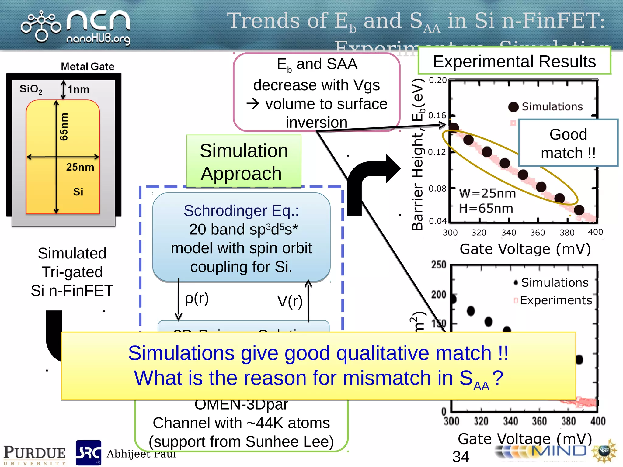
![Abhijeet Paul
Mismatch in SAA :
Interface trap density (Dit) extraction
35
A
B
3D FinFETs
bad sidewall etch [1]
interface traps
gate screened
from channel
mismatch in SAA
[1] Kapila et. al, IEEE, EDL, 2008
From
Charge
Neutrality
~2X~2X
No H2 anneal
More mismatch!!
No H2 anneal
More mismatch!!
A. Paul et. al, JAP, 2011
Difference in expt. and simulated SAA Dit extraction
Method 1
H2 anneal reduce traps by ~2X.
Difference in expt. and simulated SAA Dit extraction
Method 1
H2 anneal reduce traps by ~2X.](https://image.slidesharecdn.com/979da63d-ab42-44d9-a501-ce2e9d485a15-160110064319/75/PhD_10_2011_Abhijeet_Paul-35-2048.jpg)
![Abhijeet Paul
Mismatch in Eb :
Interface trap density (Dit) extraction
36Gate Voltage (V)
Eb(meV)
H2 anneal
H2 anneal
3D FinFETs
bad sidewall etch [1]
interface traps
gate screened
from channel
mismatch in Eb
g
b
V
E
Gate to Channel coupling.
Suppressed by interface
traps
Dit ~18.1x10¹¹
#/cm2
Dit ~15.3x10¹¹
#/cm2
[110]
Dit
~10.3x10¹¹
#/cm2
[100]Difference in expt. and simulated α Dit extraction
Method 2
[110] sidewall Dit > [100] sidewall Dit.
Difference in expt. and simulated α Dit extraction
Method 2
[110] sidewall Dit > [100] sidewall Dit.
A.Paul et. al, JAP, 2011](https://image.slidesharecdn.com/979da63d-ab42-44d9-a501-ce2e9d485a15-160110064319/75/PhD_10_2011_Abhijeet_Paul-36-2048.jpg)
![Abhijeet Paul
Porous crystalline Si for thermoelectricity
Hopkins et.al
Nano. Lett.,
2011.
Tang et.al
Nano Lett., 2010.
Yu et. al
Nature Nanotech.
2010
Electrical
Conductivity[1]
Electrical
Conductivity[1]
~1.5X Drop
Thermal
Conductivity[1]
Thermal
Conductivity[1]
~8X
Reduction
Experimental
structures
Experimental
structures
Experimental
results
Experimental
results
[1] Yu et. al Nature Nanotech., 2010.
Porous Silicon an attractive alternative for
RT thermoelectric material.
How about porous SiNWs ?
Porous Silicon an attractive alternative for
RT thermoelectric material.
How about porous SiNWs ?
47](https://image.slidesharecdn.com/979da63d-ab42-44d9-a501-ce2e9d485a15-160110064319/75/PhD_10_2011_Abhijeet_Paul-47-2048.jpg)
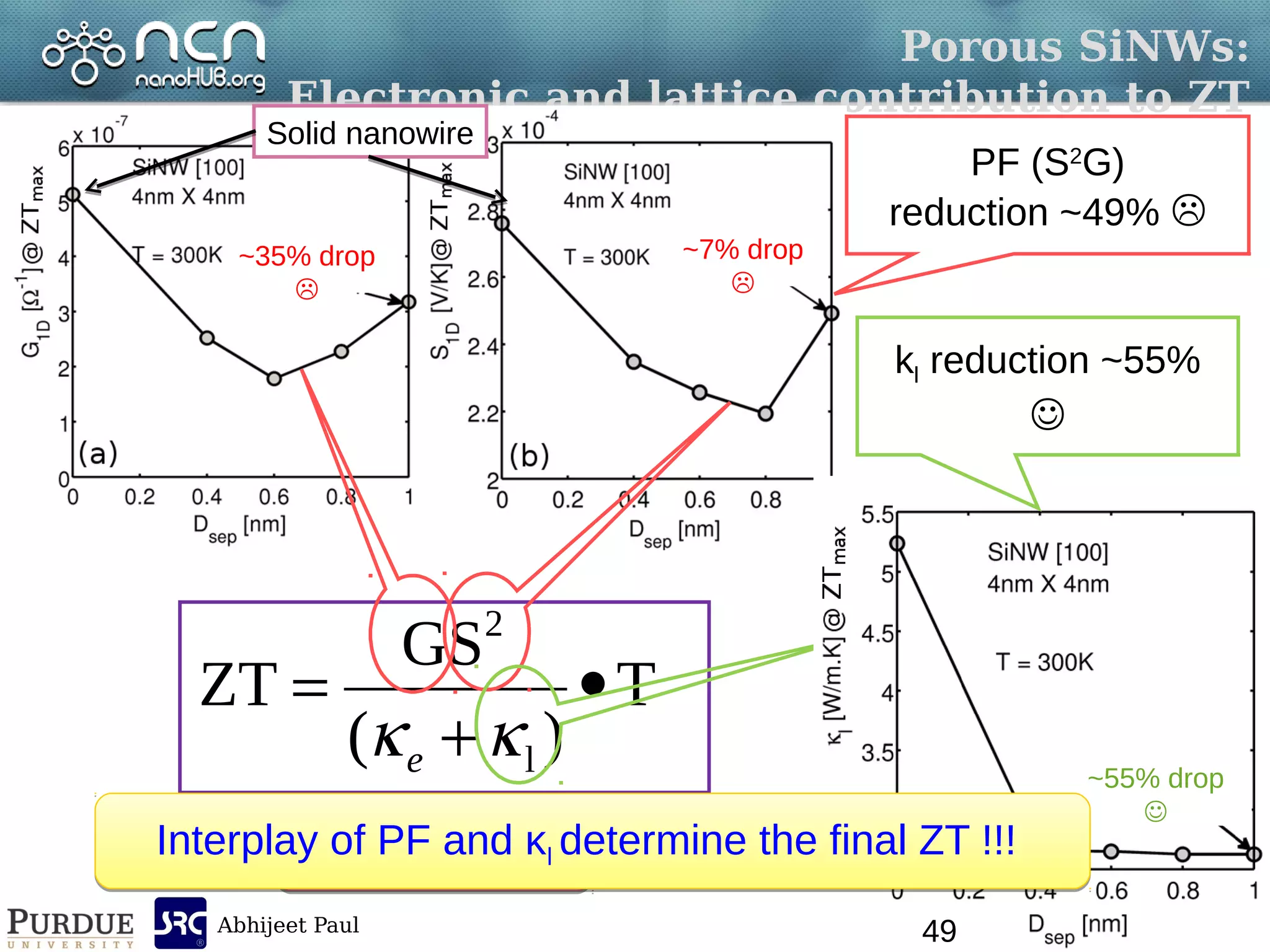
![Abhijeet Paul
Electronic and Phonon dispersion: Porous SiNW
Rh=0.4 nm
Dsep=0.2 to 1 nm
Hollow SiNW:
[100], W=4nm
Tight
Binding
Tight
Binding
Increase in Ec
more confinement
More flat bands
Suppression of
heat flow.MVFFMVFF
Increased electron and phonon confinement in
porous SiNWs compared to filled nanowire.
Increased electron and phonon confinement in
porous SiNWs compared to filled nanowire.
48](https://image.slidesharecdn.com/979da63d-ab42-44d9-a501-ce2e9d485a15-160110064319/75/PhD_10_2011_Abhijeet_Paul-48-2048.jpg)
![Abhijeet Paul
GaAs nanostructures:
Electronic and thermoelectric enhancement
54
SiNWSiNW
GaAs
[100]/(100)
~38% inc. in
ION for 4%
strain
p-type.
Integrated Modeling Approach
Integrated Modeling ApproachGa
GaAs NW
0%
2%
5%
kl = 1W/m-K [1]
~10% inc.
in ZT for
tensile strain
n-type
[1] Martin et al,
Nanoletters, 10, 2010
A. Paul et. al,
IEEE Nano,
2011
A. Paul et. al,
IEEE DRC,
2011
Integrated modeling performance enhancement of
GaAs nanostructures.
Integrated modeling performance enhancement of
GaAs nanostructures.](https://image.slidesharecdn.com/979da63d-ab42-44d9-a501-ce2e9d485a15-160110064319/75/PhD_10_2011_Abhijeet_Paul-54-2048.jpg)