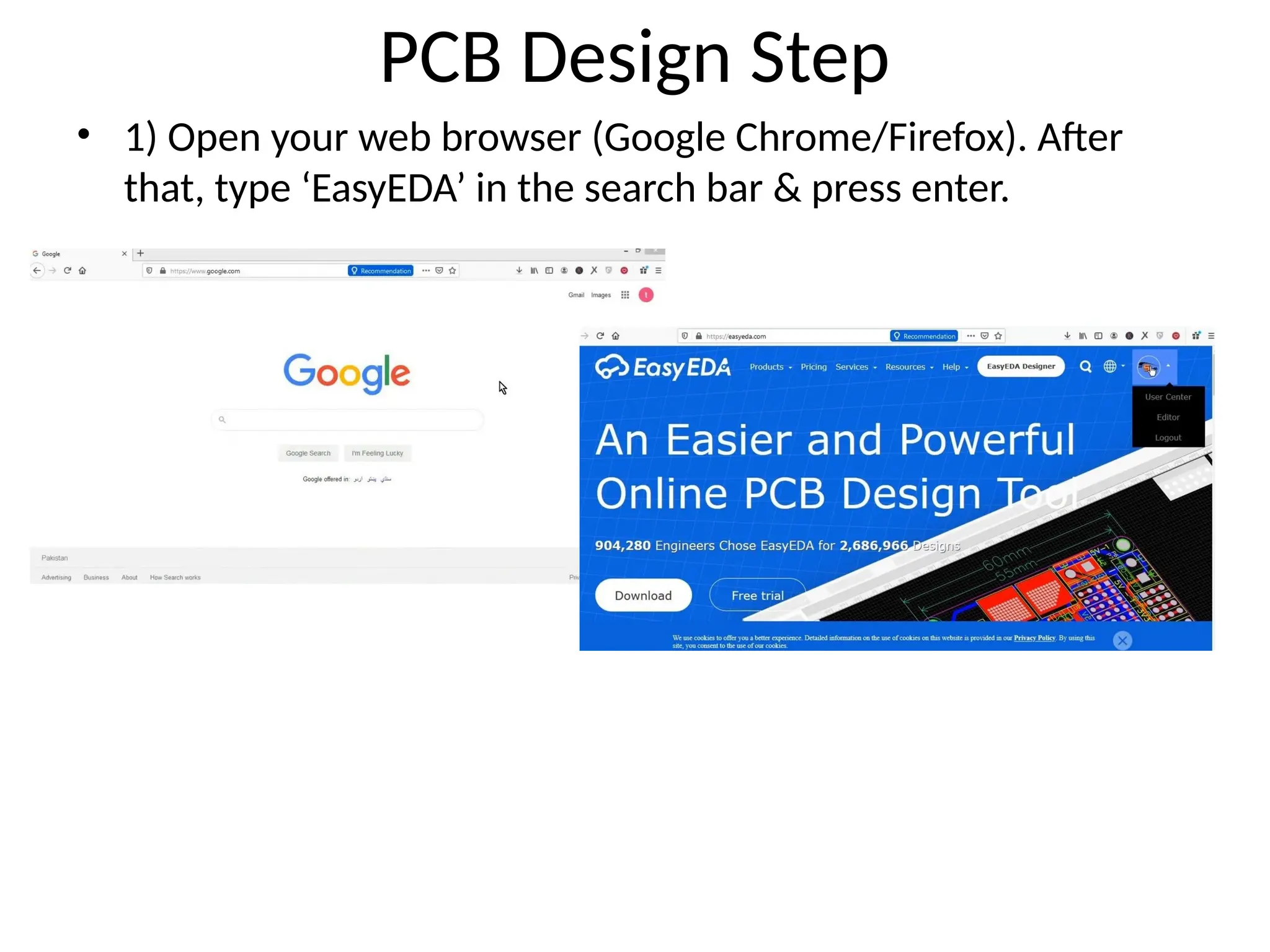
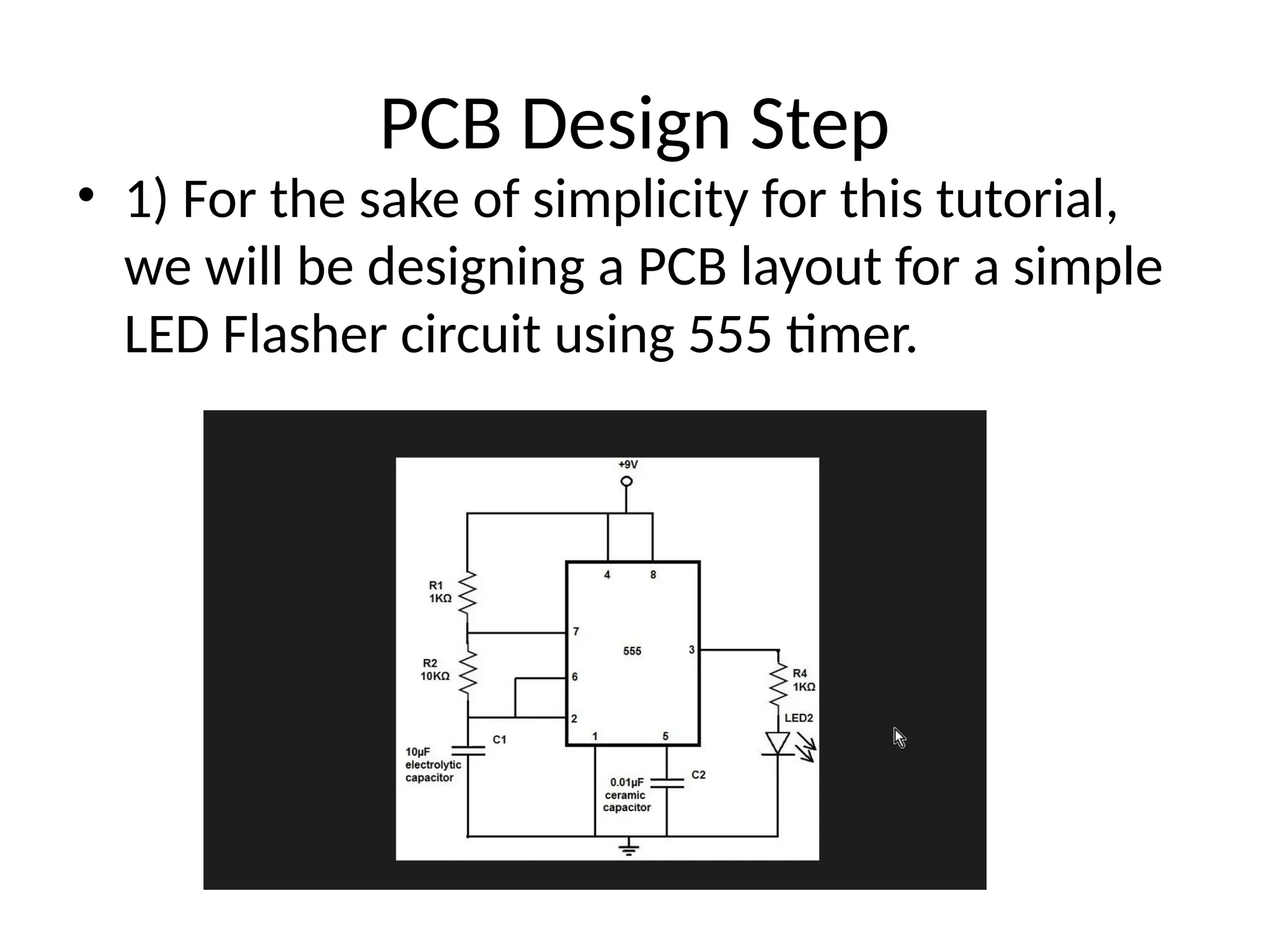
PCB Design Step
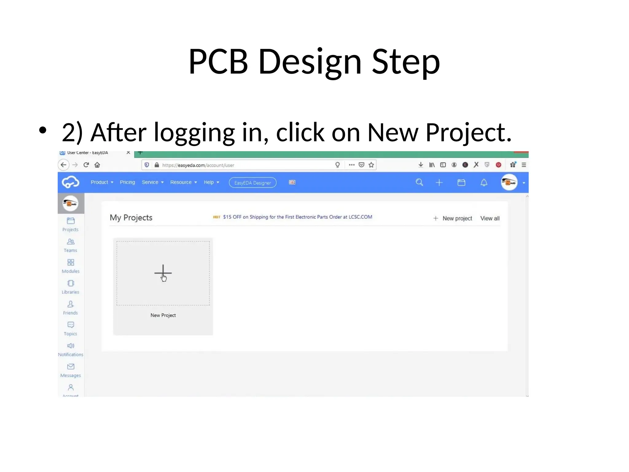
•3) After that, Set the project name &
description. After that, click on ‘Create
Project’
10.
PCB Design Step
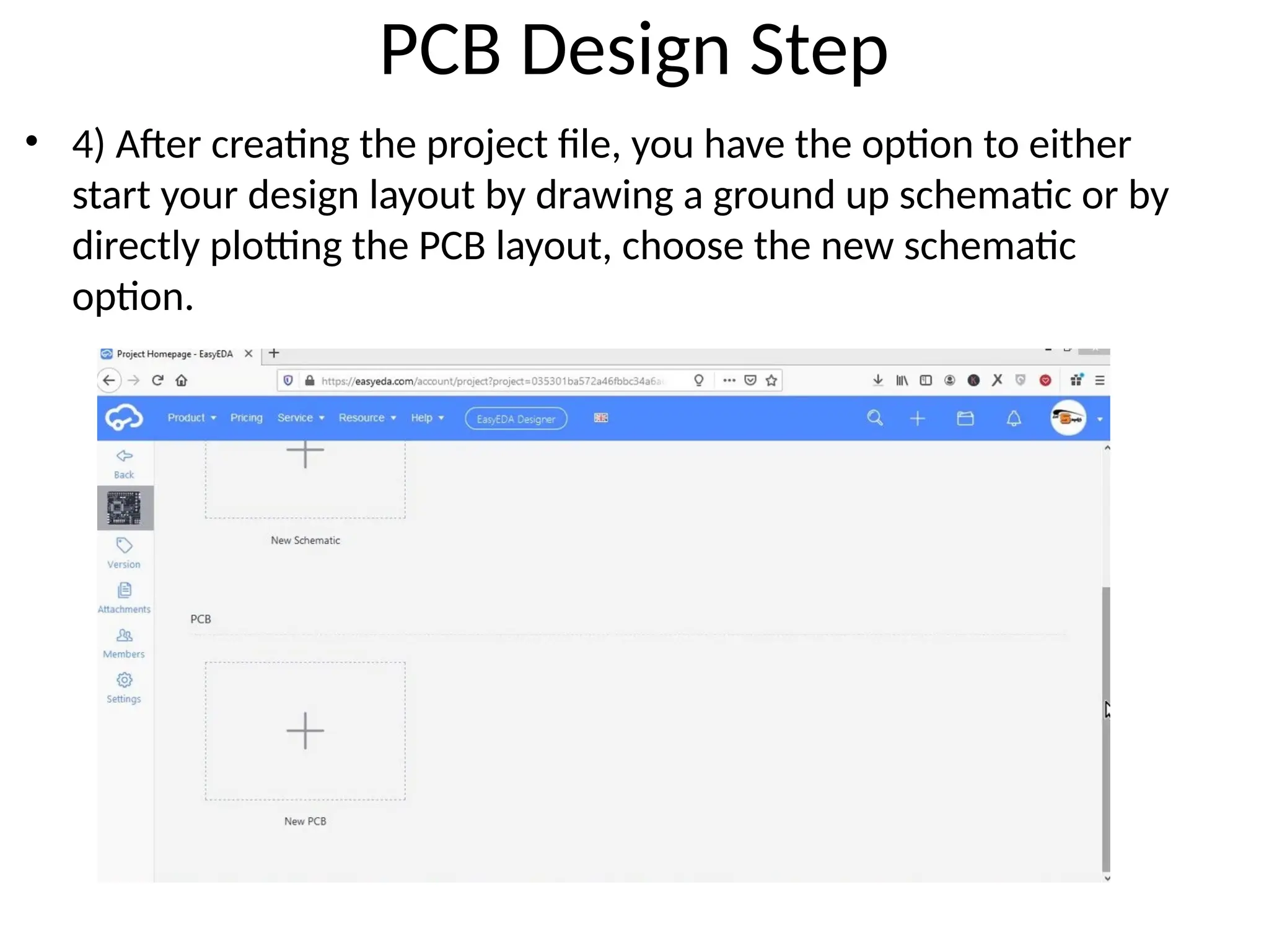
•4) After creating the project file, you have the option to either
start your design layout by drawing a ground up schematic or by
directly plotting the PCB layout, choose the new schematic
option.
11.
PCB Design Step
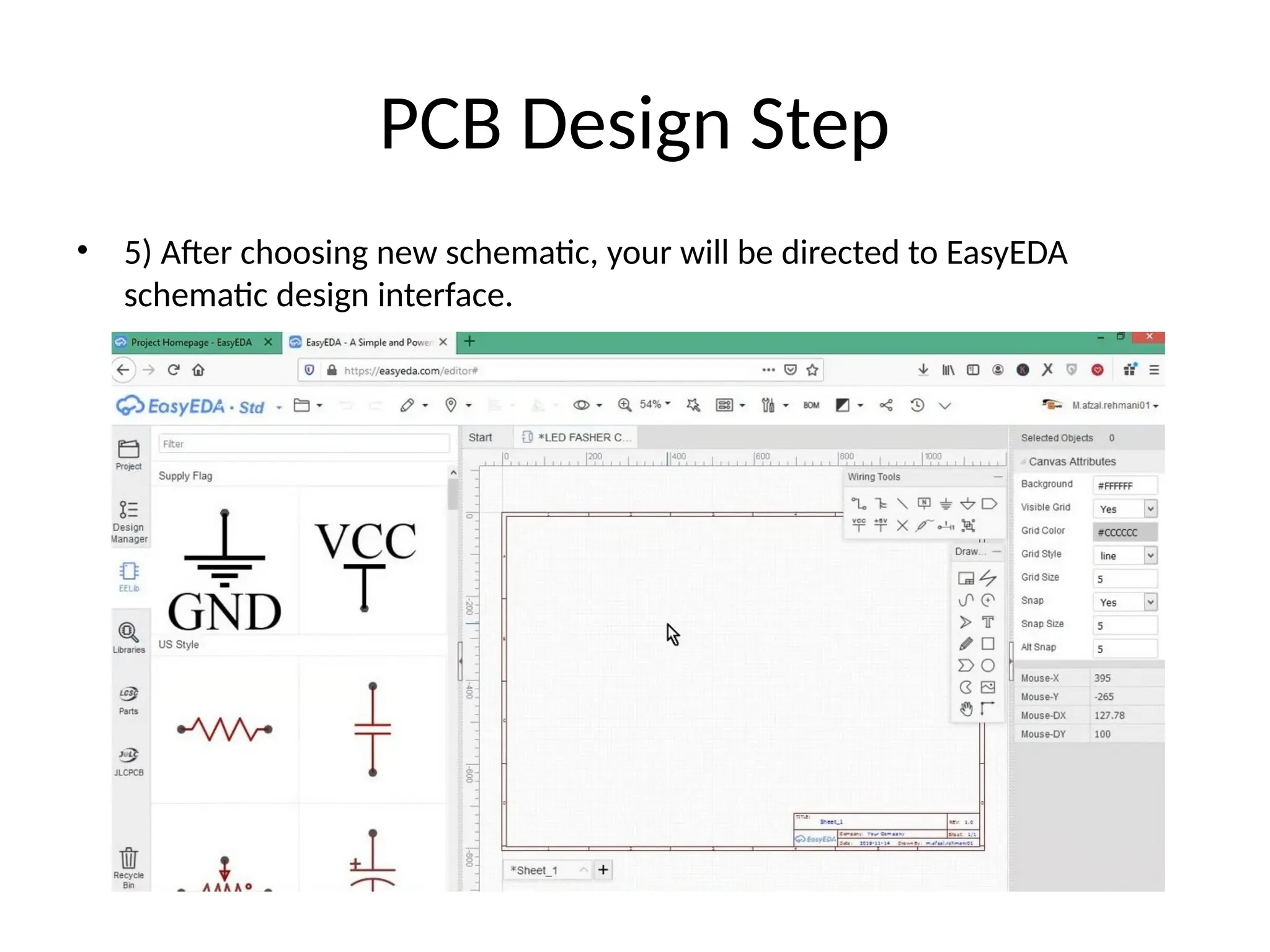
•5) After choosing new schematic, your will be directed to EasyEDA
schematic design interface.
12.
PCB Design Step
•6) You can use the component panel on the
left-side of the screen or the libraries option to
search for your desired component.
13.
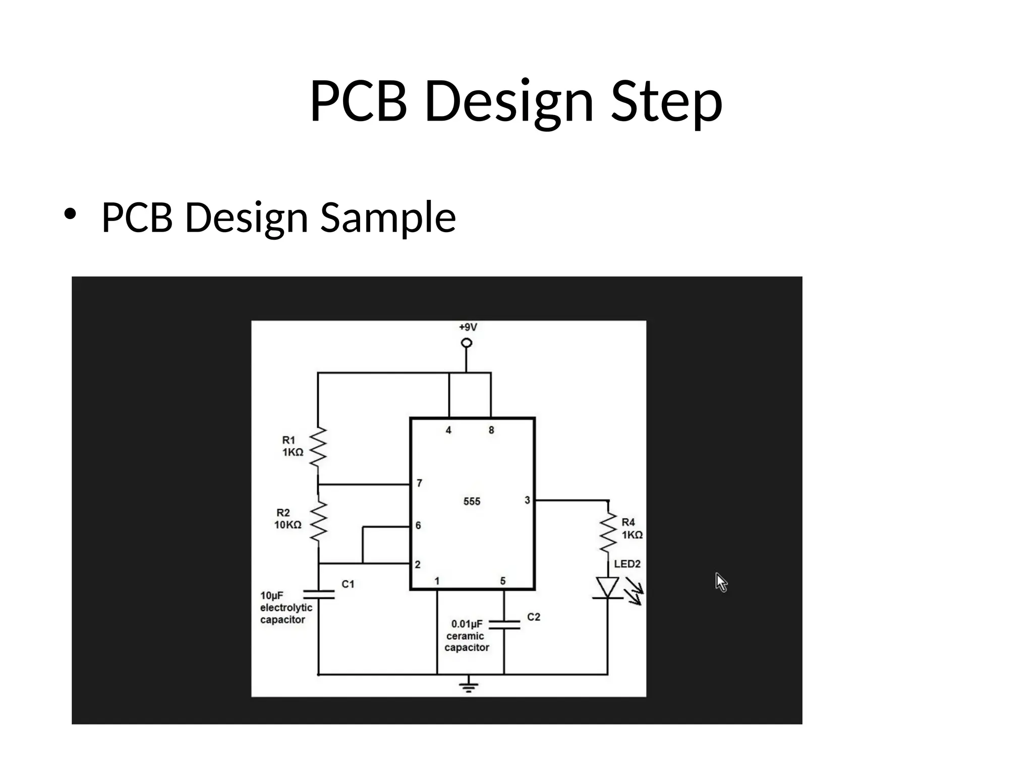
PCB Design Step
•7) Now draw the above circuit diagram in the
workspace by selecting parts from the
component list.
14.
PCB Design Step
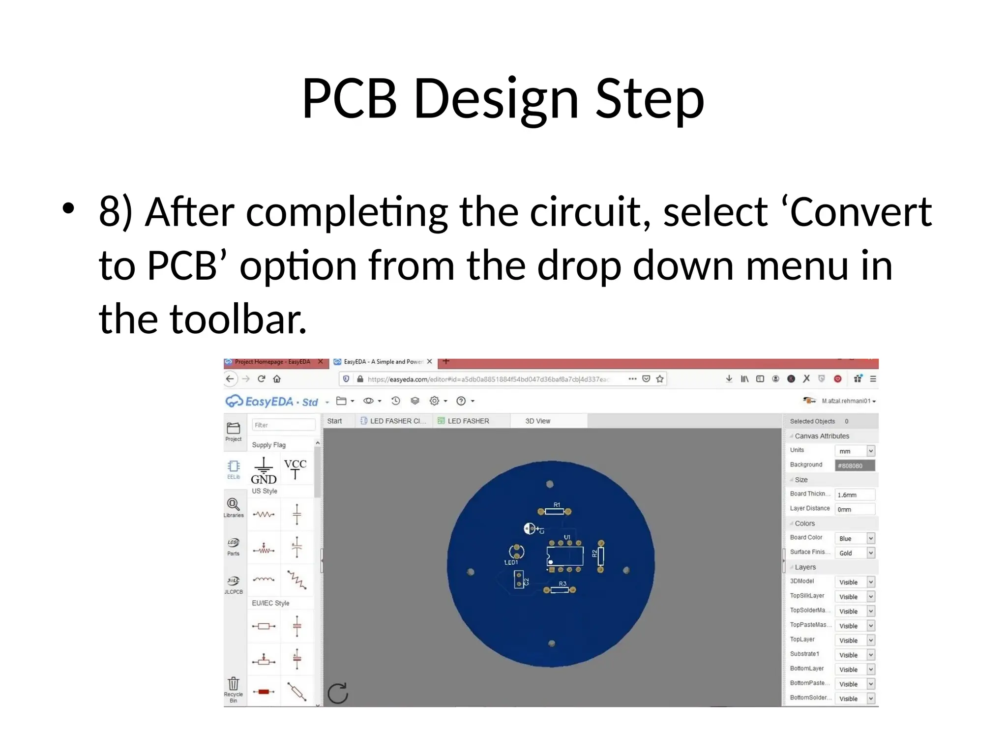
•8) After completing the circuit, select ‘Convert
to PCB’ option from the drop down menu in
the toolbar.
PCB Design Step
•1) You’ll see the PCB Layout screen with your
circuit into a rough PCB layout outside a
rectangular board outline, here select ‘mm’ in
the units menu.
PCB Design Step
•3) After that, Place all components within
board outline
19.
PCB Design Step
•4) You can also place a logo on your PCB Card
by selecting the image icon –> ‘Select image
file’ & then choose your desired image from
local drive. then drag the logo to the desired
location on the PCB board (set the image
attribute to ‘Top Silk Layer’ by right clicking &
selecting attributes).
20.
PCB Design Step
•5) After that, If you need to mount the PCB on
a device, then you can add mounting holes on
the PCB board by clicking the ‘Hole’ icon in the
PCB toolbox, then add the mounting holes.
21.
PCB Design Step
•6) After that, map copper area beneath your
PCB board outline by selecting the ‘Copper
Area’ option from the PCB toolbox & tracing
the area around the PCB Board outline and
clicking the ‘move’ hand icon.
22.
PCB Design Step
•7) After that, run the Auto router by selecting
the router option from the drop down menu.
23.
PCB Design Step
•8) After completing your design, select the 3D
view from the dropdown menu to view the
finished PCB.