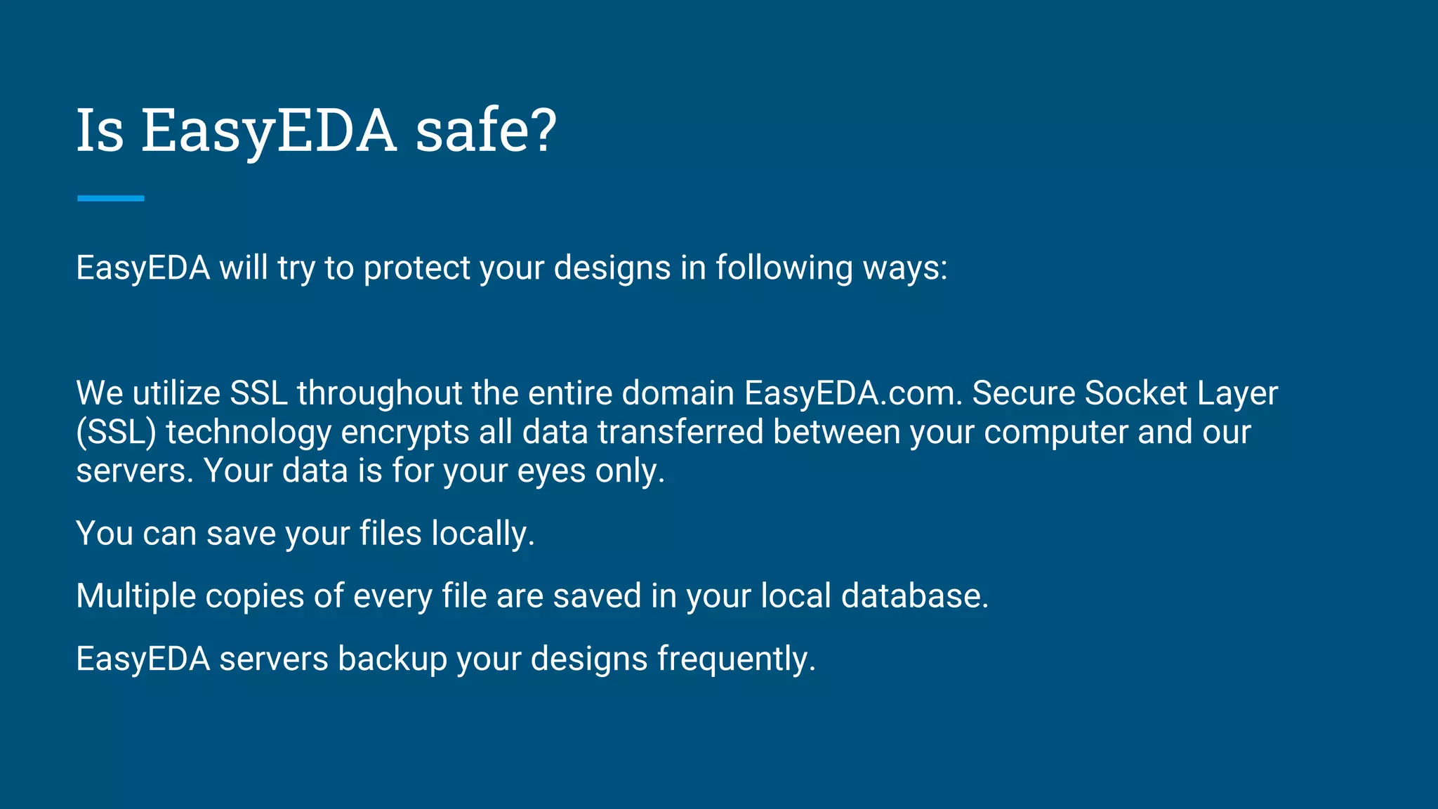
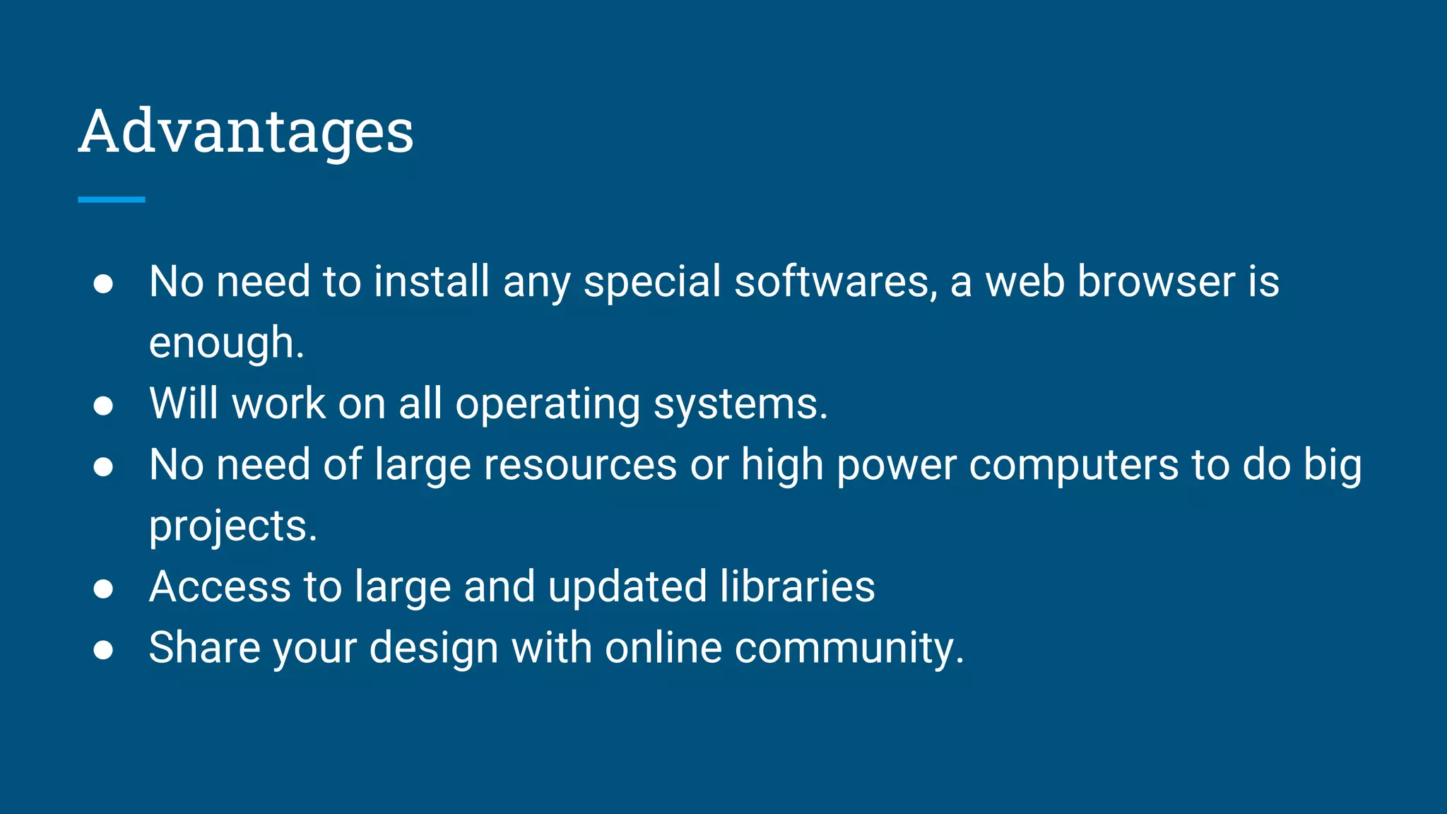
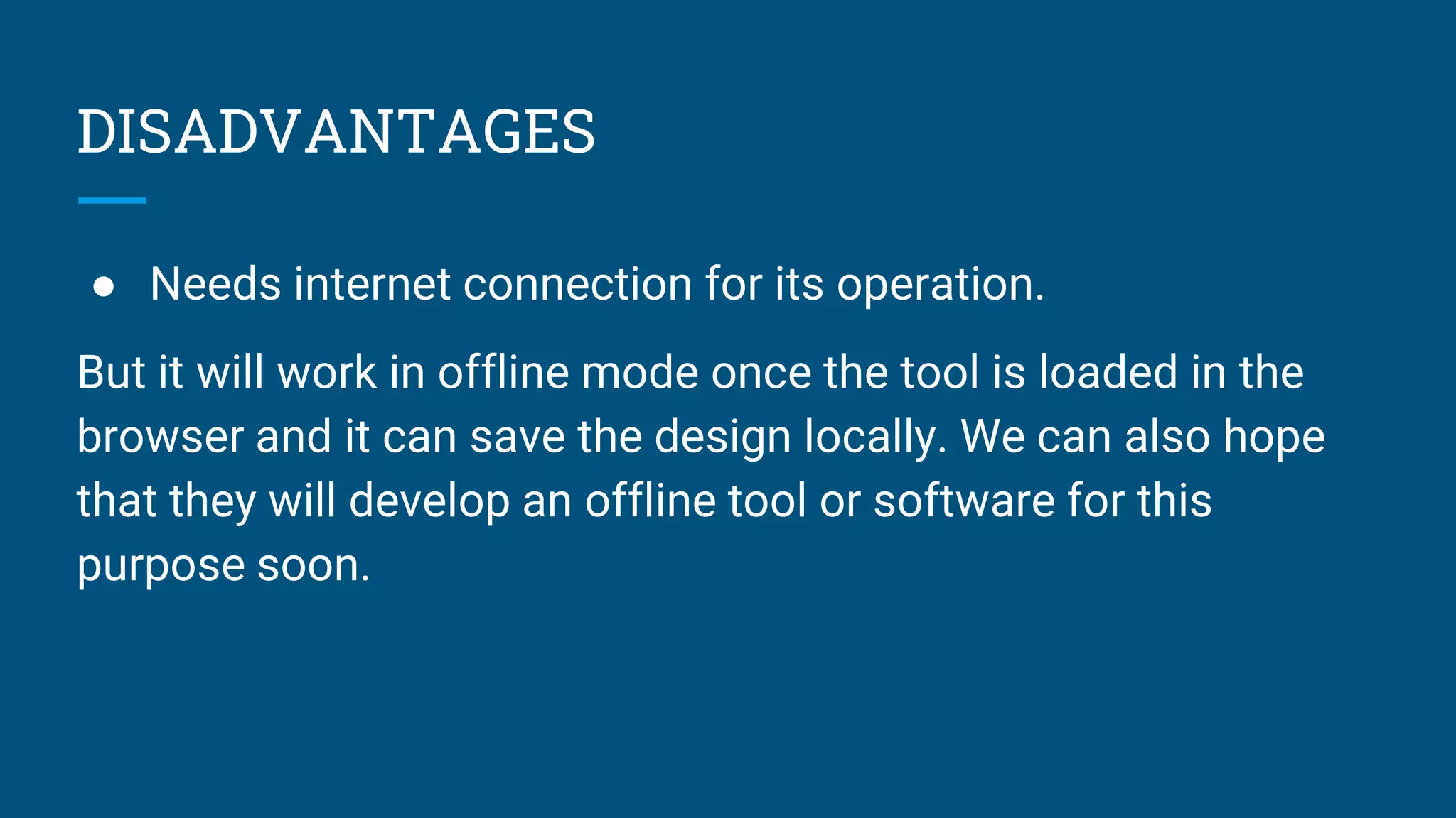
This document provides an overview and instructions for using EasyEDA, an online PCB design tool. It discusses that EasyEDA allows engineers to design, simulate, and share schematics and PCB designs publicly or privately. A step-by-step process for creating a simple PCB design in EasyEDA is outlined, including adding components to a schematic, arranging components on the board, auto-routing traces, adding copper pours, and downloading fabrication files. Key features and advantages of EasyEDA like its web-based access and integrated component libraries are highlighted. The only disadvantage mentioned is that an internet connection is needed to use the online tool.


![[BROCHURE] Italy Tour Project | @SlideON](https://cdn.slidesharecdn.com/ss_thumbnails/brochure8-251215152319-2805af68-thumbnail.jpg?width=640&height=640&fit=bounds)


