Download as PDF, PPTX
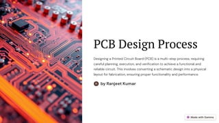
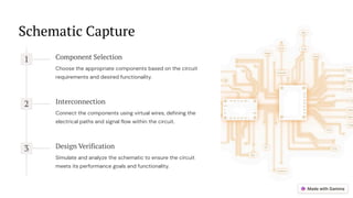

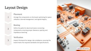
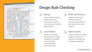
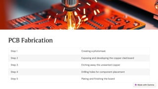
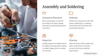
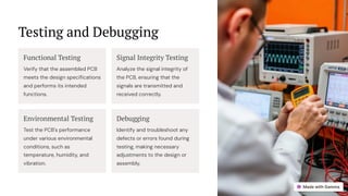
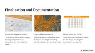

The PCB design process involves multiple steps including schematic capture, component selection, layout design, verification, and fabrication to ensure a functional and reliable circuit. Key stages include interconnecting components, verifying design rules, fabricating the board, and conducting thorough testing and debugging to meet design specifications. Documentation of the final schematic, layout, and a bill of materials is also essential for successful PCB production.