The Notes Verilog Part 2 includes the notes and keypoints of a reference book "Verilog HDL by Samir Palnitkar.
This is the second part out of the total six parts.
The PDF contains one of the six parts to learn Verilog in the simplest possible way.
It contains notes of first three chapters of the reference book Verilog HDL by Samir Palnitkar
Notes: Verilog Part 4- Behavioural ModellingJay Baxi
This is the 4th part of the Verilog HDL notes prepared from Verilog HDL by Samir Palnitkar .
It contains a broad view on behavioural modelling the second most frequently used level of abstraction needed for designing of sequential circuits.
Task and Function is the basic component of a programming language. Even on hardware Verification , those task and function is used. Task ans function provides a short way to repeatedly use the same block of code many times, This presentation gives you the basic information about Task and Function in Verilog. For more information on this, kindly contact us.
Notes: Verilog Part 5 - Tasks and FunctionsJay Baxi
The document is the penultimate part of Verilog notes out of 6 total parts.
This contains brief theoretical points on Tasks and Functions, their differences, declaration and invocation and their types and applications.
FPGA training session generic package and funtions of VHDL by Digitronix NepalKrishna Gaihre
Understanding Generic, Package and Functions in VHDL , Creating a package in VHDL, Creating Functions in VHDL is introduced in this presentation. This Training is Conducted by Digitronix Nepal. Digitronix Nepal is working on FPGA, ASIC and VLSI Design and Verification.
Java is a computer programming language that is concurrent, class-based, object-oriented, and specifically designed to have as few implementation dependencies as possible.
Radiation Hardening by Design is one of the hardware based solution to one of the most troublesome problem faced by digital circuits in the space.
RHBD provides varieties of techniques to make the circuit resilient towards such effects and ensures proper malfunctioning of the circuit.
Fundamentals of HDL (first 4 chapters only) - GodseHammam
In electronics, a hardware description language (HDL) is a specialized computer language used to program the structure, design and operation of electronic circuits, and most commonly, digital logic circuits.
MOSFETs (10EC63) Notes for Electronics & Communication Engineering Students o...Hanumantha Raju
The notes on Microelectronic Circuits (10EC63) is prepared as per VTU syllabus.
Author: M. C Hanumantharaju
Dept. of ISE, Dayananda Sagar College of Engineering
Kumaraswamy Layout, Bangalore.
Ph: 9742290764
Email: mchanumantharaju@gmail.com
For Full notes & Video Lectures contact me at the above address.
Verilog codes and testbench codes for basic digital electronic circuits. shobhan pujari
Verilog codes and test bench codes for full adder,full adder using 2 half adders,Ripple carry adder,16x1 mux using 4x1 mux,decoder,mealy state machine,counter. These are more useful for bachelor students and masters students who are pursuing degree in electrical engineering .
Microelectronic Circuits (10EC63) notes is as per the VTU Syllabus and is written from the text book authored by Sedra & Smith.
Mail your suggestions and comments to mchanumantharaju@gmail.com
Dr. M. C. Hanumantharaju,
Associate Professor
BMS Institute of Technology & Management
Bangalore
1.5 Legal Labels in Verilog areSystem Verilog extends it and al.pdfankit482504
1.
5 Legal Labels in Verilog are:
System Verilog extends it and allows one to add named blocks to reserve word end and join.
Also SystemVerilog allows to add the LABLE or NAMED BLOCK before begin, fork as below.
1.\"MY NAMED_ BLOCK\":Begin
2..\"MY NAMED_ BLOCK\":End
3..\"MY NAMED_ BLOCK\":Fork
4..\"MY NAMED_ BLOCK\":Join
5..\"MY NAMED_ BLOCK\":Initial Begin
It is illegal to have both a label before a begin or fork and a block name after the begin or fork. A
label cannot appear before the end, join, join_any or join_none, as these keywords do not form a
statement.
2.Verilog Provides in-built primitives for basic gate and switch level modeling. Any circuit can
be modeled by using continuous assignment of gate and switch level primitives.
and (strong1, weak0)#(1,2) gate1(out, in1, in2);
This is an and gate with output \'out\' and two inputs in1 and in2. Strong1 and weak0 are
optional driving strengths and gate1 is optional instance name that can be used while debugging.
First parameter in the bracket is output and you can have any number of inputs after that. This is
how you use a 3 input and gate without instance name, delay and driving strengths:
3.verilog has built in primitives like gates,transmission gates,and switches.if we need complex
primitives then verilog provides UDP or simply user defined primitives using UDP we can
model:
1.Combinational Logic
2.Sequential Logic
Verilog has 2 primitives
1.User Defined primitives
2.HDL gate primitive
4.
UDP definitions are independent of modules; they are at the same level as module definitions in
the syntax hierarchy. They can appear anywhere in the source text, either before or after they are
used inside a module. They may not appear between the keywords module and endmodule.
User-Defined Primitives(UDP) :
5. Yes it is True
One of the advanced concepts in verilog
non synthesizable
single output many iput
consume very less memory
I/Os must be scalar (i.e. bit)
1) UDPs can take only scalar input terminals (1 bit). Multiple input terminals are permitted.
2) UDPs can have only one scalar output terminal (1 bit). The output terminal must
always appear first in the terminal list. Multiple output terminals are not allowed.
3) In the declarations section, the output terminal is declared with the keyword output. Since
sequential UDPs store state, the output terminal must also be declared as a reg.
4) The inputs are declared with the keyword input.
5) The state in a sequential UDP can be initialized with an ‘initial’ statement. This statement is
optional. A 1-bit value is assigned to the output, which is declared as reg.
6) The state table entries can contain values 0,1,or x . UDPs do not handle z values. Z values
passed to a UDP are treated x values.
7)UDPs are defined at the same level as modules. UDPs can not be defined inside modules.
They can be instantiated only inside modules. UDPs are instantiated exactly like
gate primitives.
8)UDPs do not support inout ports.
6
The module is the basic unit of hier.
Those slides describe digital design using Verilog HDL,
starting with Design methodologies for any digital circuit then difference between s/w (C/C++) and H/w (Verilog) and the most important constructs that let us start hardware design using Verilog HDL.
Yaser Khalifa introduces you to VHDL (VHSIC Hardware Description Language), a hardware description language used in electronic design automation to describe digital and mixed-signal systems such as field-programmable gate arrays and integrated circuits.
CSCI 2121- Computer Organization and Assembly Language Labor.docxannettsparrow
CSCI 2121- Computer Organization and Assembly Language
Laboratory No. 5
Week of March 12th, 2018
Submission Instructions:
1. Save the files as shift.sv and vending.sv
2. Put all files into one folder.
3. Compress the folder into a .zip file.
4. Submit the zip file on Brightspace.
5. Submission Deadline: Sunday, April 15th, 2018, 11.55PM
SRC CHIP PROJECT
In order to proceed on the project for this course, there are several key Verilog concepts which are
necessary in the implementation of this code.
Part 0: More Verilog concepts.
Shared busses and tri-state buffers
Before we begin implementing the CPU, let's go over a few concepts which will be needed for the lab
assignment. The first is the concept of a shared bus. We've already seen busses in Verilog in terms of an
array of wires or registers, however in the context of our CPU, the word "bus" has another meaning. Our
CPU uses a shared "bus" which is a wire connected between the inputs and outputs of many different
registers, in order to share data:
This can be easily modelled in Verilog, using the inout keyword for a module. This defines a wire which
can act as both an input and an output to our module. However, there is one critically important design
concept which goes along with the usage of shared busses:
Only one signal can be written to a shared bus at any given time.
If two signals are written to the bus, the result is a bus collision, and the value is undefined. In the
simulation, this is represented as "X", but in real life this would cause garbage data to exist on the bus,
potentially corrupting any process which is running on the CPU. As Verilog programmers, it's our job to
ensure that a bus collision never happens. To facilitate this, we'll use a digital logic component called a
tri-state buffer:
The purpose of a tri-state buffer is to act as a switch. If B is 1, then the data can pass through the buffer,
but if not, it simply disconnects the wire, outputting a high-impedance state (in Verilog, denoted by Z).
hz943141
A B C
0 0 Z
0 1 0
1 0 Z
1 1 1
In Verilog, we can't directly write a tri-state buffer, but it can be easily synthesized using a ternary
operator as shown on line 11:
Line 11 shows the construction of a ternary operator to use as a tri-state buffer. If the input called
activate_out is set to 1, then the tri-state buffer is activated, and the circuit will put my_result on the
bus. Otherwise, it puts the value 32'bz on the bus, which will disconnect my_result from the bus, and
allow another circuit to write to the bus.
Note: It is important that during your lab assignment, any circuits which write to the bus have a tri-
state buffer implemented to prevent bus collisions.
Verilog Tasks:
Verilog tasks are like object functions in Java. Read more about them here. You may find that they are
useful in separating the code for instructions within a module, particularly for th.
The Roman Empire A Historical Colossus.pdfkaushalkr1407
The Roman Empire, a vast and enduring power, stands as one of history's most remarkable civilizations, leaving an indelible imprint on the world. It emerged from the Roman Republic, transitioning into an imperial powerhouse under the leadership of Augustus Caesar in 27 BCE. This transformation marked the beginning of an era defined by unprecedented territorial expansion, architectural marvels, and profound cultural influence.
The empire's roots lie in the city of Rome, founded, according to legend, by Romulus in 753 BCE. Over centuries, Rome evolved from a small settlement to a formidable republic, characterized by a complex political system with elected officials and checks on power. However, internal strife, class conflicts, and military ambitions paved the way for the end of the Republic. Julius Caesar’s dictatorship and subsequent assassination in 44 BCE created a power vacuum, leading to a civil war. Octavian, later Augustus, emerged victorious, heralding the Roman Empire’s birth.
Under Augustus, the empire experienced the Pax Romana, a 200-year period of relative peace and stability. Augustus reformed the military, established efficient administrative systems, and initiated grand construction projects. The empire's borders expanded, encompassing territories from Britain to Egypt and from Spain to the Euphrates. Roman legions, renowned for their discipline and engineering prowess, secured and maintained these vast territories, building roads, fortifications, and cities that facilitated control and integration.
The Roman Empire’s society was hierarchical, with a rigid class system. At the top were the patricians, wealthy elites who held significant political power. Below them were the plebeians, free citizens with limited political influence, and the vast numbers of slaves who formed the backbone of the economy. The family unit was central, governed by the paterfamilias, the male head who held absolute authority.
Culturally, the Romans were eclectic, absorbing and adapting elements from the civilizations they encountered, particularly the Greeks. Roman art, literature, and philosophy reflected this synthesis, creating a rich cultural tapestry. Latin, the Roman language, became the lingua franca of the Western world, influencing numerous modern languages.
Roman architecture and engineering achievements were monumental. They perfected the arch, vault, and dome, constructing enduring structures like the Colosseum, Pantheon, and aqueducts. These engineering marvels not only showcased Roman ingenuity but also served practical purposes, from public entertainment to water supply.
Embracing GenAI - A Strategic ImperativePeter Windle
Artificial Intelligence (AI) technologies such as Generative AI, Image Generators and Large Language Models have had a dramatic impact on teaching, learning and assessment over the past 18 months. The most immediate threat AI posed was to Academic Integrity with Higher Education Institutes (HEIs) focusing their efforts on combating the use of GenAI in assessment. Guidelines were developed for staff and students, policies put in place too. Innovative educators have forged paths in the use of Generative AI for teaching, learning and assessments leading to pockets of transformation springing up across HEIs, often with little or no top-down guidance, support or direction.
This Gasta posits a strategic approach to integrating AI into HEIs to prepare staff, students and the curriculum for an evolving world and workplace. We will highlight the advantages of working with these technologies beyond the realm of teaching, learning and assessment by considering prompt engineering skills, industry impact, curriculum changes, and the need for staff upskilling. In contrast, not engaging strategically with Generative AI poses risks, including falling behind peers, missed opportunities and failing to ensure our graduates remain employable. The rapid evolution of AI technologies necessitates a proactive and strategic approach if we are to remain relevant.
How to Make a Field invisible in Odoo 17Celine George
It is possible to hide or invisible some fields in odoo. Commonly using “invisible” attribute in the field definition to invisible the fields. This slide will show how to make a field invisible in odoo 17.
June 3, 2024 Anti-Semitism Letter Sent to MIT President Kornbluth and MIT Cor...Levi Shapiro
Letter from the Congress of the United States regarding Anti-Semitism sent June 3rd to MIT President Sally Kornbluth, MIT Corp Chair, Mark Gorenberg
Dear Dr. Kornbluth and Mr. Gorenberg,
The US House of Representatives is deeply concerned by ongoing and pervasive acts of antisemitic
harassment and intimidation at the Massachusetts Institute of Technology (MIT). Failing to act decisively to ensure a safe learning environment for all students would be a grave dereliction of your responsibilities as President of MIT and Chair of the MIT Corporation.
This Congress will not stand idly by and allow an environment hostile to Jewish students to persist. The House believes that your institution is in violation of Title VI of the Civil Rights Act, and the inability or
unwillingness to rectify this violation through action requires accountability.
Postsecondary education is a unique opportunity for students to learn and have their ideas and beliefs challenged. However, universities receiving hundreds of millions of federal funds annually have denied
students that opportunity and have been hijacked to become venues for the promotion of terrorism, antisemitic harassment and intimidation, unlawful encampments, and in some cases, assaults and riots.
The House of Representatives will not countenance the use of federal funds to indoctrinate students into hateful, antisemitic, anti-American supporters of terrorism. Investigations into campus antisemitism by the Committee on Education and the Workforce and the Committee on Ways and Means have been expanded into a Congress-wide probe across all relevant jurisdictions to address this national crisis. The undersigned Committees will conduct oversight into the use of federal funds at MIT and its learning environment under authorities granted to each Committee.
• The Committee on Education and the Workforce has been investigating your institution since December 7, 2023. The Committee has broad jurisdiction over postsecondary education, including its compliance with Title VI of the Civil Rights Act, campus safety concerns over disruptions to the learning environment, and the awarding of federal student aid under the Higher Education Act.
• The Committee on Oversight and Accountability is investigating the sources of funding and other support flowing to groups espousing pro-Hamas propaganda and engaged in antisemitic harassment and intimidation of students. The Committee on Oversight and Accountability is the principal oversight committee of the US House of Representatives and has broad authority to investigate “any matter” at “any time” under House Rule X.
• The Committee on Ways and Means has been investigating several universities since November 15, 2023, when the Committee held a hearing entitled From Ivory Towers to Dark Corners: Investigating the Nexus Between Antisemitism, Tax-Exempt Universities, and Terror Financing. The Committee followed the hearing with letters to those institutions on January 10, 202
Welcome to TechSoup New Member Orientation and Q&A (May 2024).pdfTechSoup
In this webinar you will learn how your organization can access TechSoup's wide variety of product discount and donation programs. From hardware to software, we'll give you a tour of the tools available to help your nonprofit with productivity, collaboration, financial management, donor tracking, security, and more.
Operation “Blue Star” is the only event in the history of Independent India where the state went into war with its own people. Even after about 40 years it is not clear if it was culmination of states anger over people of the region, a political game of power or start of dictatorial chapter in the democratic setup.
The people of Punjab felt alienated from main stream due to denial of their just demands during a long democratic struggle since independence. As it happen all over the word, it led to militant struggle with great loss of lives of military, police and civilian personnel. Killing of Indira Gandhi and massacre of innocent Sikhs in Delhi and other India cities was also associated with this movement.
Model Attribute Check Company Auto PropertyCeline George
In Odoo, the multi-company feature allows you to manage multiple companies within a single Odoo database instance. Each company can have its own configurations while still sharing common resources such as products, customers, and suppliers.
Adversarial Attention Modeling for Multi-dimensional Emotion Regression.pdf
Notes: Verilog Part 2 - Modules and Ports - Structural Modeling (Gate-Level Modeling)
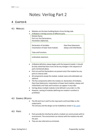
1. 1|Page
Notes: Verilog Part 2
4 CHAPTER 4:
4.1 MODULES:
Modules are the basic building blocks of any Verilog code.
A Module in Verilog consists of different parts.
Module Name,
Port List, Port Declarations,
Parameters (Optional),
Declaration of Variables
Instantiation of lower level modules
Data Flow Statements
always and initial blocks.
Tasks and Functions.
endmodule statement.
A Module definition always begins with the keyword module. It should
be duly noted that there must not be any changes in the sequence of
parts mentioned above.
Port List and Port Declarations are present only if the module has any
ports to interact with.
All components except the module, module name and endmodule are
optional.
The five components within the module viz. Declaration of Varibales,
Data Flow Statements, Instantiation of lower level modules, always and
initial blocks and Tasks and Functions can appear in any order.
Verilog allows multiple modules to be defined in any order in a file.
However, nesting of modules (defining one module in another) is
prohibited.
4.2 EXAMPLE: SR LATCH
The SR Latch has S and R as the input ports and Q and Qbar as the
output ports.
The stimulus and the design can be modelled as shown in SR_Latch
Ports provide the interface by which a module can communicate with its
environment. The environment can interact with the module only with
the port.
They are also referred to as terminals.
4.3 PORTS
Notes: Verilog Part-2
Prepared By: Jay Baxi
2. 2|Page
4.4 LIST OF PORTS:
A module definition can optionally have a list of ports. If module does
not need to exchange any signals with the environment, there are no
ports in the list.
In case of a top level module TOP, which has a full adder module
4fulladd. The module 4fulladd takes input a, b, c_in as inputs and
produces sum and c_out as outputs.
The top level module does not need to pass or receive signals. Thus it
does not have a list of ports.
4.5 PORT DECLARATION
All ports in the list of ports must be declared in the module.
They can be input (input port), output (output port) or inout port
(bidirectional port).
By default these ports are declared as wire.
However, if output holds their value, they must be declared as reg.
For example, in D_FF, when q was supposed to retain its value after a
clock edge.
Ports of input and inout cannot be declared as reg because reg variables
are supposed to store values and input ports should not store values but
simply reflect the changes in the external signals they are connected to.
(ERROR)
Internal
External
Inputs
net
reg/net
Outputs
reg/net
reg
Inouts
net
net
Width Matching: It is legal to connect internal and external items of
different sizes when making inter-module port connections. A warning is
usually displayed that widths do not match.
Unconnected ports: Verilog allows the ports to remain unconnected. For
ports that are used only for debugging, it can be remained unconnected.
The module, in this case can be instantiated by
4fulladd(SUM, , A, B, C_in) // port C_out is unconnected
4.6 CONNECTING PORTS TO EXTERNAL SIGNALS
Notes: Verilog Part-2
There are two methods to connect ports to external signals
1.) Connecting Ports by ordered lists:
The signals to be connected must appear in the module instantiation in the
same order as the ports in the port list in the module definition
2.) Connecting Ports by name:
For large modules, it is not feasible to remember the order of each port.
Hence, in those cases, Verilog provides connecting external signals to ports
by the port names.
Prepared By: Jay Baxi
3. 3|Page
5 CHAPTER 5:
5.1 TRUTH TABLES OF LOGIC GATES
5.1.1
5.1.2
5.1.3
5.1.4
5.1.5
AND Gate
AND
0
1
X
Z
0
0
0
0
0
1
0
1
X
X
X
0
X
X
X
Z
0
X
X
X
OR Gate
OR
0
1
X
Z
0
0
1
X
X
1
1
1
1
1
X
X
1
X
X
Z
X
1
X
X
NAND Gate
NAND
0
1
X
Z
0
1
1
1
1
1
1
0
X
X
X
1
X
X
X
Z
1
X
X
X
NOR Gate
NOR
0
1
X
Z
0
1
0
X
X
1
0
0
0
0
X
X
0
X
X
Z
X
0
X
X
XOR Gate
XOR
0
1
X
Z
0
0
1
X
X
1
1
0
X
X
X
X
X
X
X
Z
X
X
X
X
Notes: Verilog Part-2
Prepared By: Jay Baxi
4. 4|Page
5.1.6
5.1.7
XNOR Gate
XNOR
0
1
X
Z
0
1
0
X
X
1
0
1
X
X
Z
X
X
X
X
BUF Gate and NOT Gate
In
0
1
X
Z
5.1.8
X
X
X
X
X
BUF
0
1
X
X
NOT
1
0
X
X
BUFif and NOTif
The BUFif and NOTif are the gates that propagate only if their control
signal is asserted. They propagate Z if the signal is deasserted.
These signals are used when a signal is driven only when the control
signal is asserted, this is a case when multiple drivers drive the signal
//Instantiation of gates
bufif1 b1 (out, in, ctrl);
bufif0 b0 (out, in, ctrl);
notif1 n1(out, in, ctrl);
notif0 n0(out, in, ctrl);
The Truth Tables of these gates are given as follows
Bufif1
0
1
X
Z
0
Z
Z
Z
Z
1
0
1
X
X
X
L
H
X
X
Z
L
H
X
X
Bufif0
0
1
X
Z
0
0
1
X
Z
1
Z
Z
Z
Z
X
L
H
X
X
Z
L
H
X
X
Notif1
0
1
X
Z
0
Z
Z
Z
Z
1
1
0
X
X
X
H
L
X
X
Z
H
L
X
X
Notes: Verilog Part-2
Prepared By: Jay Baxi
5. 5|Page
Notif0
0
1
X
Z
5.1.9
0
1
0
X
X
Array of Instances
1
Z
Z
Z
Z
X
H
L
X
X
Z
H
L
X
X
For situations when there are more than one instances required, Verilog
allows us to create array of instances where each instance differs from
other just by the index.
5.1.10 Examples:
5.1.10.1 Gate Level Multiplexer
We will design a 4-to-1 Mux with 2 select signals. Using the basic logic gates the logic
diagram of a 4-to-1 Mux is given as follows
The Verilog modules for the same are given in Multiplexer
5.1.10.2 4-bit Ripple Carry Adder
A 4-bit full adder can be created from four 1-bit FA. The Verilog modules for the same is
given in Full Adder.
5.2 GATE DELAYS
Rise delay is when a delay is experienced while transition from 0, X or Z to 1.
Fall delay is when a delay is experienced while transition from 1, X or Z to 0.
Turn off delay is associated with a gate output transition to high impedance
(Z) value from another value.
Notes: Verilog Part-2
Prepared By: Jay Baxi
6. 6|Page
Notes: Verilog Part-2
Min value: The minimum value of delay, the designer expects to have.
Max value: The maximum value of delay, the designer expects to have.
Typ value: The typical value of delay, the designer expects to have.
Prepared By: Jay Baxi