Downloaded 21 times
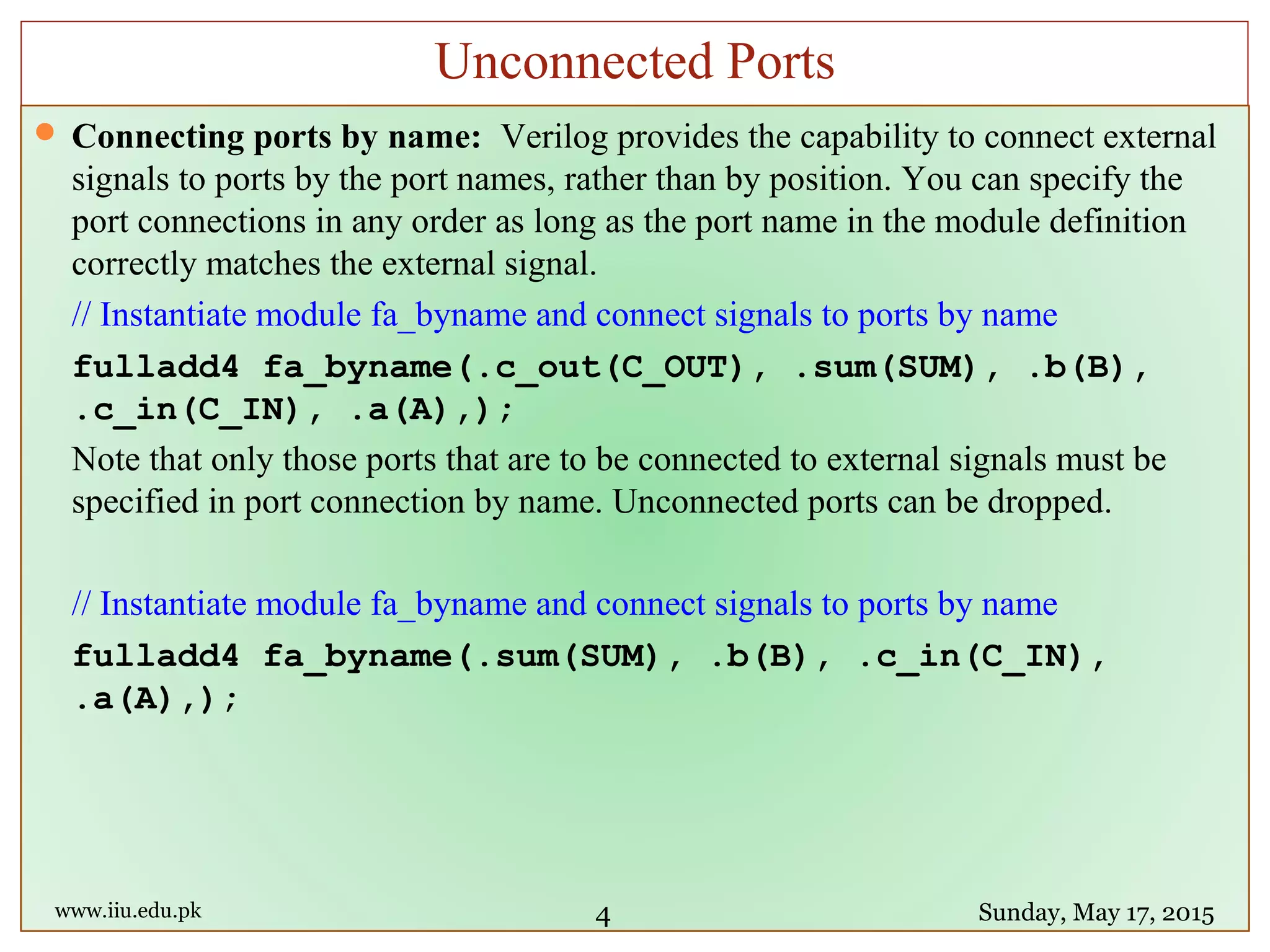
![ There are two methods of making connections between signals specified in the
module instantiation and the ports in a module definition. These two methods
cannot be mixed. These methods are a follows
Connecting by ordered list: The signals to be connected must appear in the
module instantiation in the same order as the ports in the port list in the module
definition.
module top;
reg [3:0]A,B; reg C_IN; wire [3:0] SUM; wire C_OUT;
// Signals are connected to ports in order (by position)
fulladd4 fa_ordered(SUM, C_OUT, A, B, C_IN);
endmodule
module fulladd4 (sum, c_out, a, b, c_in);
output[3:0] sum; output c_cout;
input [3:0] a, b; input c_in;
<module internals>
endmodule
www.iiu.edu.pk Sunday, May 17, 2015
Unconnected Ports
3](https://image.slidesharecdn.com/fpga-07-port-rules-gate-delay-data-flow-carry-look-ahead-adder-150517184249-lva1-app6891/75/Fpga-07-port-rules-gate-delay-data-flow-carry-look-ahead-adder-3-2048.jpg)
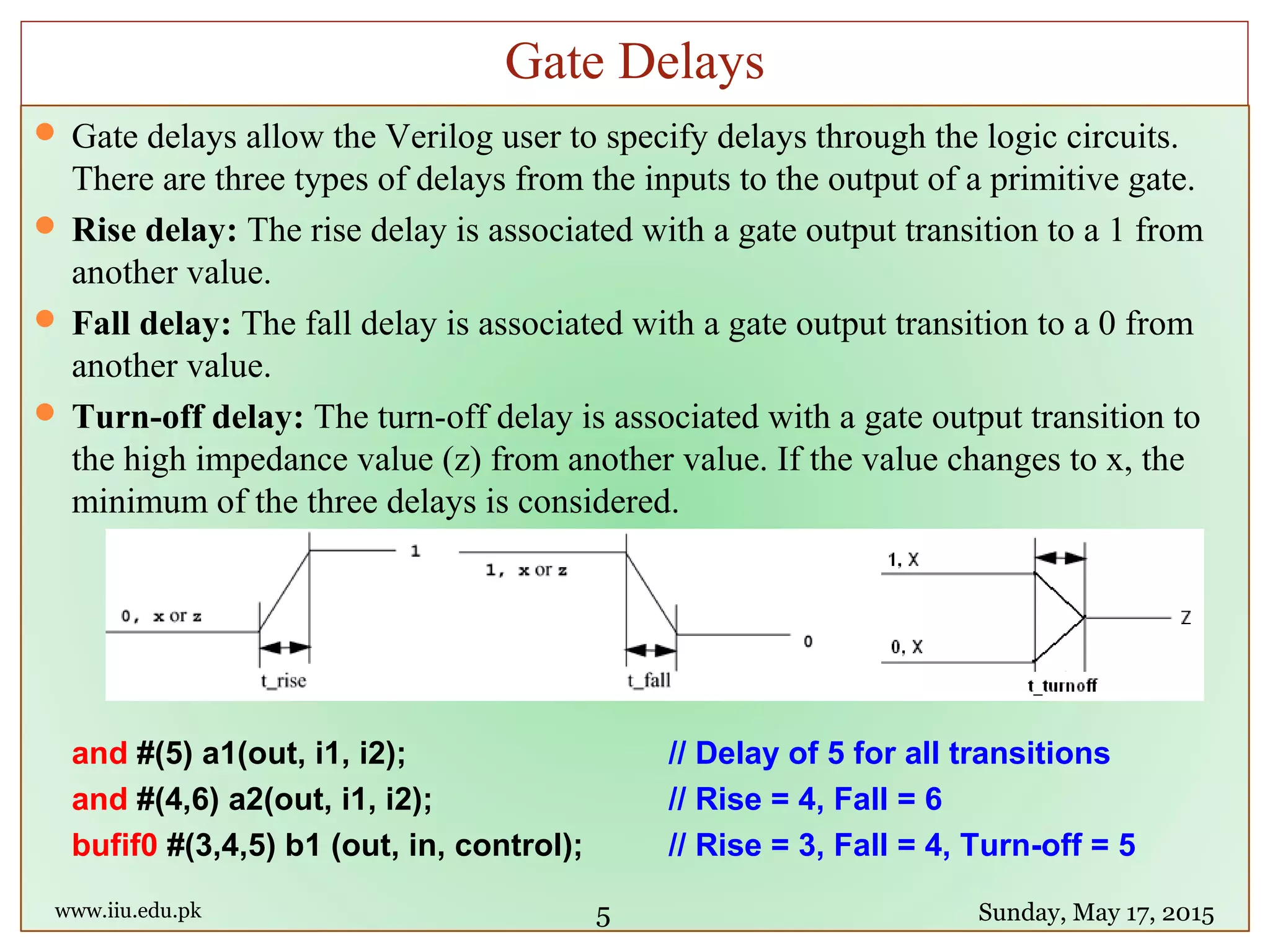
![ For small circuits, the gate-level modeling approach works very well
Verilog allows a circuit to be designed in terms of the data flow between registers
and how a design processes data rather than instantiation of individual gates.
With gate densities on chips increasing rapidly, dataflow modeling has assumed
great importance.
Currently, automated tools are used to create a gate-level circuit from a dataflow
design description. This process is called logic synthesis.
In the digital design community, the term RTL (Register Transfer Level) design is
commonly used for a combination of dataflow modeling and behavioral
modeling.
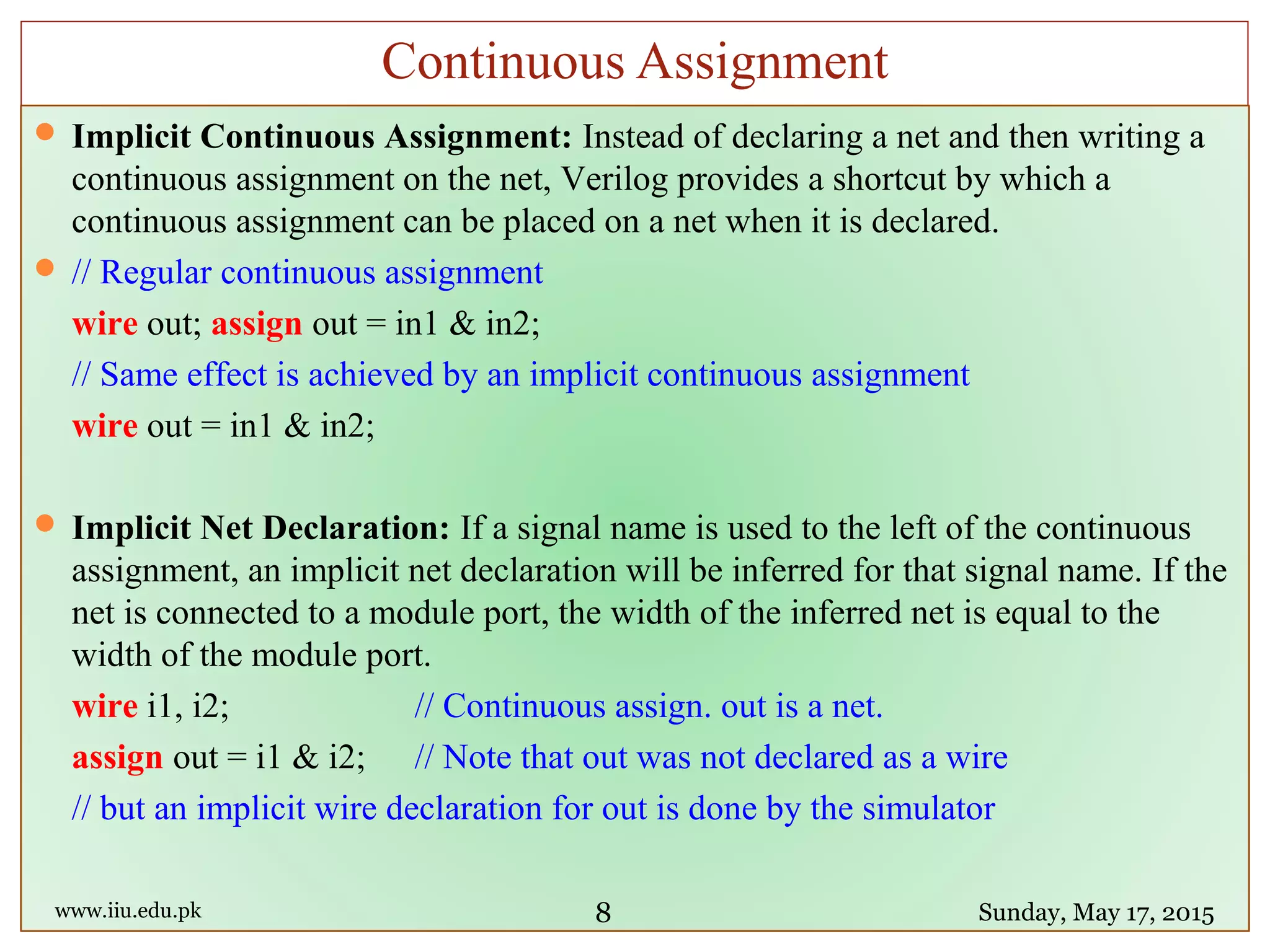
Continuous Assignments:
assign out = i1 & i2; // Continuous assign. out is a net. i1 and i2 are nets.
assign addr[15:0] = addr1_bits[15:0] ^ addr2_bits[15:0];
assign {c_out, sum[3:0]} = a[3:0] + b[3:0] + c_in;
// if right side changes the output is recalculated and assigned to the left variable
// Note: the variable on the left hand side will be a net. It can not be a reg.
// The variables on right hand side can be a net or a reg value.www.iiu.edu.pk Sunday, May 17, 2015
Continuous Assignment
7](https://image.slidesharecdn.com/fpga-07-port-rules-gate-delay-data-flow-carry-look-ahead-adder-150517184249-lva1-app6891/75/Fpga-07-port-rules-gate-delay-data-flow-carry-look-ahead-adder-7-2048.jpg)
![ The concatenation operator ( {, } ) provides a mechanism to append multiple
operands. The operands must be sized.
Unsized operands are not allowed because the size of each operand must be
known for computation of the size of the result.
Concatenations are expressed as operands within braces, with commas separating
the operands. Operands can be scalar nets or registers, vector nets or registers, bit-
select, part-select, or sized constants.
A = 1'b1, B = 2'b00, C = 2'b10, D = 3'b110
Y = {B , C} // Result Y is 4'b0010
Y = {A , B , C , D , 3'b001} // Result Y is 11'b 1_00_10_110_001
Y = {A , B[0], C[1]} // Result Y is 3'b101
www.iiu.edu.pk Sunday, May 17, 2015
Concatenation Operators
18](https://image.slidesharecdn.com/fpga-07-port-rules-gate-delay-data-flow-carry-look-ahead-adder-150517184249-lva1-app6891/75/Fpga-07-port-rules-gate-delay-data-flow-carry-look-ahead-adder-18-2048.jpg)
![ Repetitive concatenation of the same number can be expressed by using a
replication constant.
A replication constant specifies how many times to replicate the number inside
the brackets ( { } ).
reg A;
reg [1:0] B, C;
reg [2:0] D;
A = 1'b1; B = 2'b00; C = 2'b10; D = 3'b110;
Y = { 4{A} } // Result Y is 4'b1111
Y = { 4{A} , 2{B} } // Result Y is 8'b11110000
Y = { 4{A} , 2{B} , C } // Result Y is 8'b1111000010
www.iiu.edu.pk Sunday, May 17, 2015
Replication Operators
19](https://image.slidesharecdn.com/fpga-07-port-rules-gate-delay-data-flow-carry-look-ahead-adder-150517184249-lva1-app6891/75/Fpga-07-port-rules-gate-delay-data-flow-carry-look-ahead-adder-19-2048.jpg)
![// Module 4-to-1 multiplexer using data flow. Conditional operator.
module multiplexer4_to_1 (out, i0, i1, i2, i3, s1, s0);
output out; input i0, i1, i2, i3, s1, s0;
// Use nested conditional operator
assign out = s1 ? ( s0 ? i3 : i2) : (s0 ? i1 : i0) ;
endmodule
// Define a 4-bit full adder by using dataflow statements.
module fulladd4(sum, c_out, a, b, c_in);
output [3:0] sum; output c_out;
input[3:0] a, b; input c_in;
// Specify the function of a full adder
assign {c_out, sum} = a + b + c_in;
endmodule
www.iiu.edu.pk Sunday, May 17, 2015
Data Flow Examples
21](https://image.slidesharecdn.com/fpga-07-port-rules-gate-delay-data-flow-carry-look-ahead-adder-150517184249-lva1-app6891/75/Fpga-07-port-rules-gate-delay-data-flow-carry-look-ahead-adder-21-2048.jpg)
![module fulladd4(sum, c_out, a, b, c_in);
// Inputs and outputs
output [3:0] sum;
output c_out;
input [3:0] a,b;
input c_in;
// Internal wires
wire p0,g0, p1,g1, p2,g2, p3,g3;
wire c4, c3, c2, c1;
// compute the p(carry propagation) for each stage
assign p0 = a[0] ^ b[0],
p1 = a[1] ^ b[1],
p2 = a[2] ^ b[2],
p3 = a[3] ^ b[3];
// compute the g (carry generator) for each stage
assign g0 = a[0] & b[0],
g1 = a[1] & b[1],
g2 = a[2] & b[2],
g3 = a[3] & b[3];
www.iiu.edu.pk Sunday, May 17, 2015
Carrey Look Ahead Adder
27](https://image.slidesharecdn.com/fpga-07-port-rules-gate-delay-data-flow-carry-look-ahead-adder-150517184249-lva1-app6891/75/Fpga-07-port-rules-gate-delay-data-flow-carry-look-ahead-adder-27-2048.jpg)
![// compute the carry for each stage Note that c_in is
// equivalent c0 in the arithmetic equation for carry
// look-ahead computation
assign c1 = g0 | (p0 & c_in),
c2 = g1 | (p1 & g0) | (p1 & p0 & c_in);
assign c3 = g2 | (p2 & g1) |
(p2 & p1 & g0) |
(p2 & p1 & p0 & c_in);
assign c4 = g3 | (p3 & g2) | (p3 & p2 & g1) |
(p3 & p2 & p1 & g0) |
(p3 & p2 & p1 & p0 & c_in);
// Compute Sum
assign sum[0] = p0 ^ c_in,
sum[1] = p1 ^ c1,
sum[2] = p2 ^ c2,
sum[3] = p3 ^ c3;
assign c_out = c4; // Assign carry output
endmodule
www.iiu.edu.pk Sunday, May 17, 2015
Carrey Look Ahead Adder
28](https://image.slidesharecdn.com/fpga-07-port-rules-gate-delay-data-flow-carry-look-ahead-adder-150517184249-lva1-app6891/75/Fpga-07-port-rules-gate-delay-data-flow-carry-look-ahead-adder-28-2048.jpg)

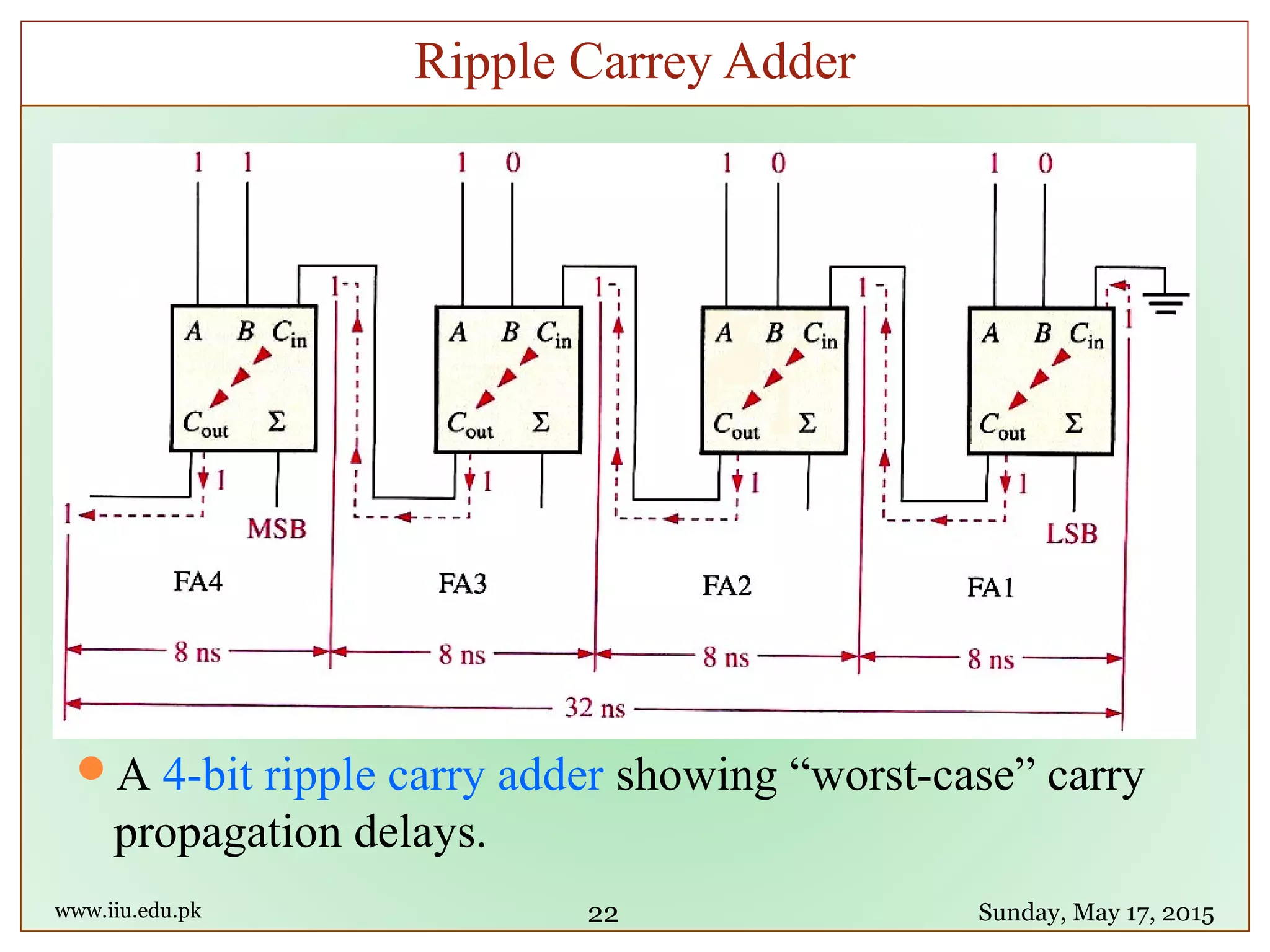
The document discusses various topics related to Verilog including: 1. Port connection rules in Verilog modules can connect signals by ordered list or by name. Width matching between modules is allowed but may generate warnings. 2. Gate delays in Verilog allow specification of rise, fall, and turn-off delays for logic gates. Minimum, typical, and maximum delay values can also be provided. 3. Data flow modeling in Verilog describes a circuit in terms of data flow between registers rather than individual gates. This level of abstraction is known as register transfer level (RTL) modeling.