Download as PDF, PPTX

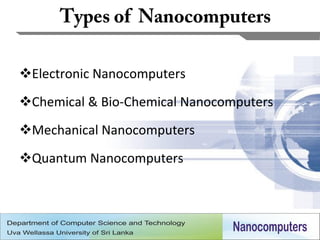

The document discusses various types of proposed nanocomputers including electronic, chemical, mechanical, and quantum nanocomputers. Electronic nanocomputers would operate similarly to microcomputers today but on a smaller physical scale using nanolithography. Chemical and mechanical nanocomputers would store and process information via chemical interactions or mechanical positioning of atoms. Quantum nanocomputers would use atomic quantum states like electron spin to store data. Realizing these proposed nanocomputers remains challenging but would allow computing at the molecular level.


