M.Sridevi, Dr P.Sudhakar Reddy / International Journal of Engineering Research and
                      Applications (IJERA) ISSN: 2248-9622 www.ijera.com
                      Vol. 2, Issue 5, September- October 2012, pp.2217-2219

           Design And Implementation Of Hdlc Protocol On Fpga
                              M.Sridevi*, Dr P.Sudhakar Reddy**
        *(Department of ECE, Srikalasthiswara institute of technology, Srikalasthi, Chittor, Andhra Pradesh)
       **(Department of ECE, Srikalasthiswara institute of technology, Srikalasthi, Chittor, Andhra Pradesh)


ABSTRACT
         High-level Data Link Control (HDLC)                 programmed repeatedly. Considering speed and
procedure is one of the most important protocols             flexibility, FPGA can process multi-channel signals
in digital and data communication system                     in parallel, and the real-time capacity is predictable
development. HDLC procedures are the high-                   and able to be simulated.
level data link control procedures established by
ISO, which are widely used in digital                         II.     HDLC Module
communication and are the bases of many other                          HDLC procedures can be implemented in
data link control protocols. HDLC procedures                 FPGA by hardware programming. By adopting
are commonly performed by FPGA/ASIC devices                  hardware processing technology, FPGA devices can
and embedded software programming. Here we                   be programmed repeatedly. Considering speed and
are proposing new implementation of HDLC                     flexibility, FPGA can process multi-channel signals
protocol for sensor network data processing                  in parallel, and the real-time capacity is predictable
system design and implementation based on Low                and able to be simulated.
power FPGA Architecture. The over all System
Architecture will be designed using Veri-log and
simulation, synthesis and implementation
(Translation, Mapping, Placing and Routing) will
be done using various FPGA based EDA Tools
like Xilings. Finally the proposed system
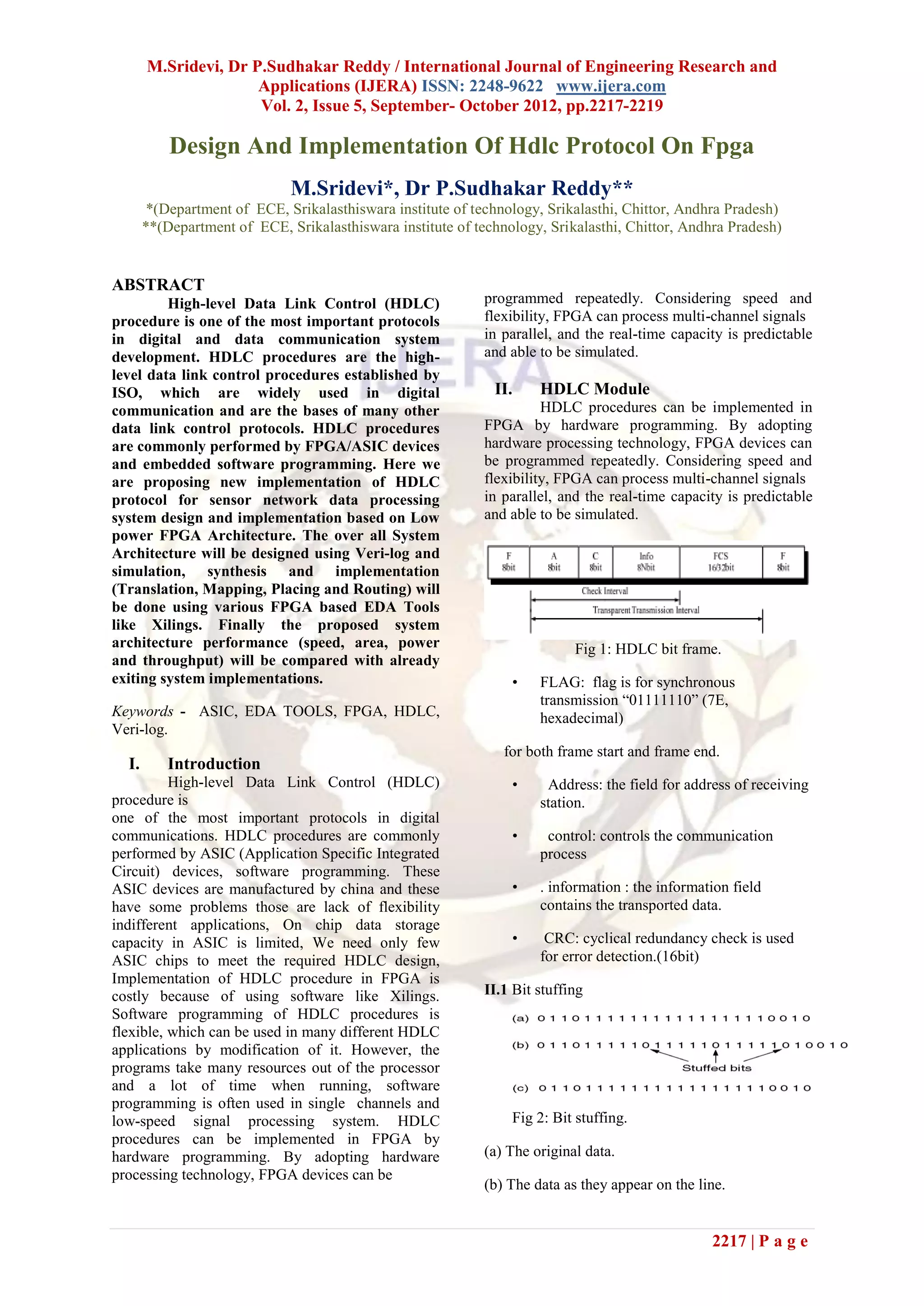
architecture performance (speed, area, power                                Fig 1: HDLC bit frame.
and throughput) will be compared with already
exiting system implementations.                                  •    FLAG: flag is for synchronous
                                                                      transmission “01111110” (7E,
Keywords - ASIC, EDA TOOLS, FPGA, HDLC,                               hexadecimal)
Veri-log.
                                                                for both frame start and frame end.
  I.       Introduction
          High-level Data Link Control (HDLC)                    •     Address: the field for address of receiving
procedure is                                                          station.
one of the most important protocols in digital
communications. HDLC procedures are commonly                     •     control: controls the communication
performed by ASIC (Application Specific Integrated                    process
Circuit) devices, software programming. These
ASIC devices are manufactured by china and these                 •    . information : the information field
have some problems those are lack of flexibility                      contains the transported data.
indifferent applications, On chip data storage
capacity in ASIC is limited, We need only few                    •     CRC: cyclical redundancy check is used
ASIC chips to meet the required HDLC design,                          for error detection.(16bit)
Implementation of HDLC procedure in FPGA is
costly because of using software like Xilings.               II.1 Bit stuffing
Software programming of HDLC procedures is
flexible, which can be used in many different HDLC
applications by modification of it. However, the
programs take many resources out of the processor
and a lot of time when running, software
programming is often used in single channels and
low-speed signal processing system. HDLC                         Fig 2: Bit stuffing.
procedures can be implemented in FPGA by
hardware programming. By adopting hardware                   (a) The original data.
processing technology, FPGA devices can be
                                                             (b) The data as they appear on the line.


                                                                                                  2217 | P a g e
M.Sridevi, Dr P.Sudhakar Reddy / International Journal of Engineering Research and
                    Applications (IJERA) ISSN: 2248-9622 www.ijera.com
                    Vol. 2, Issue 5, September- October 2012, pp.2217-2219
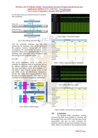
(c) The data as they are stored in receiver’s memory
after unstuffing.


                                                                     Fig 5: HDLC Transmitter output.

           Fig 3: Bit stuffing and removing.

And the proposed technique has the new
architecture by including some of the techniques
like pipeline, resource sharing and will further
investigating the optimization of various system
parameters (area, power, throughput, etc). Even I am
including some application (Network Sensor Data
Processing) for this proposed system.

II.2 CSC

The cyclic redundancy check, or CRC, is a                    Table 1: HDLC transmitter device utilization.
technique for detecting errors in digital data, but not
for making corrections when errors are detected.
The user data which should be a multiple of 8
bits;”CRCL” and “CRCM” are the 8 bits of LSB
and MSB of 16 bit CRC(Cyclic Redundancy
Check). The frame check sequence(FCS) to check
the data transmission reliability. The FCS is zero
insertion and removal for transparent transmission.


                                                                       Fig 6: HDLC Receiver output.


            Fig 4: HDLC module design.
                                                                 Table 2: HDLC receiver device utilization.

                                                          III.      Conclusion
                                                                   We designed HDLC procedures’ sending
                                                          and receiving RTL level modules in Veri-log, and
                                                          downloaded them into FPGA and had them tested
                                                          successfully, and also we have overcome the
                                                          problems existed in the previous technique that uses
                                                          ASIC which is not flexible so this proposed method


                                                                                                2218 | P a g e
M.Sridevi, Dr P.Sudhakar Reddy / International Journal of Engineering Research and
                       Applications (IJERA) ISSN: 2248-9622 www.ijera.com
                       Vol. 2, Issue 5, September- October 2012, pp.2217-2219
can be more useful for many applications like a
Communication protocol link for RADAR data
processing . Real time embedded sensor data and
transmission procedures. Basic communication
protocol controller in embedded SOC. Various
Material sensor wireless data processing system.

VI.       Acknowledgements
         The author M. Sridevi thankful to
Associative Professor Sri Dr.P.Sudhakar Reddy for
his valuable suggestions.

References
  [1]     Henriksson T, Dake Liu, “Implementation
          of fast CRC calculation,” Proceedings of
          the Asia and South Pacific, Design
          Automatation Conference, pp 563-564,
          January 2003.
  [2]     Ming-Der Shieh, Hsin-Fu Lo, Ming-Hwa
          Sheu, “High-speed generation of LFSR
          signatures,” Processdings of Ninth Asia,
          Test Symposium, pp 222-227, December
          2000.
  [3]     Mitel Semiconductor, “MT8952B HDLC
          Protocol Controller,” Mitel Semiconductor
          Inc., pp 2-14, May 1997
  [4]     ISO/IEC 13239, “Information technology -
          -Telecommunications and Information
          exchange between systems – High-level
          data link control (HDLC) procedures,”
          International       Organization      for
          Standardization, pp 10-17, July 2002.
  [6]     Li Wang, “Computer Network Practical
          Guide”, Beijing: Tsinghua University
          Press, pp 72-78, 2007. (in Chinese)


                                                                                 2219 | P a g e

Mx2522172219

  • 1.
    M.Sridevi, Dr P.SudhakarReddy / International Journal of Engineering Research and Applications (IJERA) ISSN: 2248-9622 www.ijera.com Vol. 2, Issue 5, September- October 2012, pp.2217-2219 Design And Implementation Of Hdlc Protocol On Fpga M.Sridevi*, Dr P.Sudhakar Reddy** *(Department of ECE, Srikalasthiswara institute of technology, Srikalasthi, Chittor, Andhra Pradesh) **(Department of ECE, Srikalasthiswara institute of technology, Srikalasthi, Chittor, Andhra Pradesh) ABSTRACT High-level Data Link Control (HDLC) programmed repeatedly. Considering speed and procedure is one of the most important protocols flexibility, FPGA can process multi-channel signals in digital and data communication system in parallel, and the real-time capacity is predictable development. HDLC procedures are the high- and able to be simulated. level data link control procedures established by ISO, which are widely used in digital II. HDLC Module communication and are the bases of many other HDLC procedures can be implemented in data link control protocols. HDLC procedures FPGA by hardware programming. By adopting are commonly performed by FPGA/ASIC devices hardware processing technology, FPGA devices can and embedded software programming. Here we be programmed repeatedly. Considering speed and are proposing new implementation of HDLC flexibility, FPGA can process multi-channel signals protocol for sensor network data processing in parallel, and the real-time capacity is predictable system design and implementation based on Low and able to be simulated. power FPGA Architecture. The over all System Architecture will be designed using Veri-log and simulation, synthesis and implementation (Translation, Mapping, Placing and Routing) will be done using various FPGA based EDA Tools like Xilings. Finally the proposed system architecture performance (speed, area, power Fig 1: HDLC bit frame. and throughput) will be compared with already exiting system implementations. • FLAG: flag is for synchronous transmission “01111110” (7E, Keywords - ASIC, EDA TOOLS, FPGA, HDLC, hexadecimal) Veri-log. for both frame start and frame end. I. Introduction High-level Data Link Control (HDLC) • Address: the field for address of receiving procedure is station. one of the most important protocols in digital communications. HDLC procedures are commonly • control: controls the communication performed by ASIC (Application Specific Integrated process Circuit) devices, software programming. These ASIC devices are manufactured by china and these • . information : the information field have some problems those are lack of flexibility contains the transported data. indifferent applications, On chip data storage capacity in ASIC is limited, We need only few • CRC: cyclical redundancy check is used ASIC chips to meet the required HDLC design, for error detection.(16bit) Implementation of HDLC procedure in FPGA is costly because of using software like Xilings. II.1 Bit stuffing Software programming of HDLC procedures is flexible, which can be used in many different HDLC applications by modification of it. However, the programs take many resources out of the processor and a lot of time when running, software programming is often used in single channels and low-speed signal processing system. HDLC Fig 2: Bit stuffing. procedures can be implemented in FPGA by hardware programming. By adopting hardware (a) The original data. processing technology, FPGA devices can be (b) The data as they appear on the line. 2217 | P a g e
  • 2.
    M.Sridevi, Dr P.SudhakarReddy / International Journal of Engineering Research and Applications (IJERA) ISSN: 2248-9622 www.ijera.com Vol. 2, Issue 5, September- October 2012, pp.2217-2219 (c) The data as they are stored in receiver’s memory after unstuffing. Fig 5: HDLC Transmitter output. Fig 3: Bit stuffing and removing. And the proposed technique has the new architecture by including some of the techniques like pipeline, resource sharing and will further investigating the optimization of various system parameters (area, power, throughput, etc). Even I am including some application (Network Sensor Data Processing) for this proposed system. II.2 CSC The cyclic redundancy check, or CRC, is a Table 1: HDLC transmitter device utilization. technique for detecting errors in digital data, but not for making corrections when errors are detected. The user data which should be a multiple of 8 bits;”CRCL” and “CRCM” are the 8 bits of LSB and MSB of 16 bit CRC(Cyclic Redundancy Check). The frame check sequence(FCS) to check the data transmission reliability. The FCS is zero insertion and removal for transparent transmission. Fig 6: HDLC Receiver output. Fig 4: HDLC module design. Table 2: HDLC receiver device utilization. III. Conclusion We designed HDLC procedures’ sending and receiving RTL level modules in Veri-log, and downloaded them into FPGA and had them tested successfully, and also we have overcome the problems existed in the previous technique that uses ASIC which is not flexible so this proposed method 2218 | P a g e
  • 3.
    M.Sridevi, Dr P.SudhakarReddy / International Journal of Engineering Research and Applications (IJERA) ISSN: 2248-9622 www.ijera.com Vol. 2, Issue 5, September- October 2012, pp.2217-2219 can be more useful for many applications like a Communication protocol link for RADAR data processing . Real time embedded sensor data and transmission procedures. Basic communication protocol controller in embedded SOC. Various Material sensor wireless data processing system. VI. Acknowledgements The author M. Sridevi thankful to Associative Professor Sri Dr.P.Sudhakar Reddy for his valuable suggestions. References [1] Henriksson T, Dake Liu, “Implementation of fast CRC calculation,” Proceedings of the Asia and South Pacific, Design Automatation Conference, pp 563-564, January 2003. [2] Ming-Der Shieh, Hsin-Fu Lo, Ming-Hwa Sheu, “High-speed generation of LFSR signatures,” Processdings of Ninth Asia, Test Symposium, pp 222-227, December 2000. [3] Mitel Semiconductor, “MT8952B HDLC Protocol Controller,” Mitel Semiconductor Inc., pp 2-14, May 1997 [4] ISO/IEC 13239, “Information technology - -Telecommunications and Information exchange between systems – High-level data link control (HDLC) procedures,” International Organization for Standardization, pp 10-17, July 2002. [6] Li Wang, “Computer Network Practical Guide”, Beijing: Tsinghua University Press, pp 72-78, 2007. (in Chinese) 2219 | P a g e