Downloaded 11 times
![International Journal of Modern Engineering Research (IJMER)
www.ijmer.com Vol. 3, Issue. 1, Jan.-Feb. 2013 pp-12-18 ISSN: 2249-6645
Design and Implementation of HDLC Controller by Using
Crc-16
Gaurav Chandil1, Priyanka Mishra2
1, 2
(Department of Electronics and Communication Engineering, United Group of Institutions, Allahabad, India)
ABSTRACT: HDLC controller megacell is a high performance module for the bit oriented, switched, non-switched packet
transmission module. The controller fulfills the specifications according to ITU q.921, X.25 level 2 recommendations. It
supports half duplex and full duplex communication lines, point-to-point and multipoint channels. Furthermore, the
controller is designed to permit synchronous, code transparent data transmission. The control information is always in the
same position and specific bit patterns used for control differ dramatically from those representing data that reduces the
chances of errors. The data stream and transmission rate is controlled by the network node. In this paper, we have designed,
simulated and implemented HDLC controller .This design is coded in a hardware description language (VHDL). The
function of coded design is to simulate on simulation software (e.g. modelsim). After simulation, the design is synthesized
and translated into a structural architecture, in terms of the components on the target FPGA device (Spartan 3) and perform
the post-translate simulation in order to ensure the proper functioning of the design after translation. After the successful
simulation of the post-translate model, the design is mapped to the existing slices of the FPGA and the post-map model
simulated. The post-map model does not include the routing delays. The objective of this paper is to run the programmed
FPGA at frequency i.e. it Operates up to 155.52 Mbits/s data rates.In this paper, we implemented the various HDLC
controllers for 16-bit address, 8 bit data and 16 bit CRC Check, simulation result for final output at the receiver end for 8-
bit data16-bit address and 16-bit CRC, with bit stuffing and removal of error in HDLC.
Keywords: High Level Data Link Control (HDLC) Controller, Frame Check Sequence (FCS), Cyclic Redundancy Check
(CRC), Synchronous Data Link Control (SDLC).
I. INTRODUCTION
HDLC (High-level Data Link Control) is a group of protocols for transmitting synchronous data packets between
point to point nodes. In this controller, data is organized into frames. HDLC protocol resides with Layer 2 of the OSI model ,
the data link layer. It make use of zero insertion/deletion process (bit stuffing) to ensure that the bit pattern of the delimiter
flag does not occur in the fields between flags. The HDLC frame is synchronous and therefore relies on the physical layer to
provide method of clocking and synchronizing the transmission and reception of frames paper.
HDLC controller is one of the most important data link control protocols which are widely used for high
performance. It is the basis for many other important data link control protocols, such as LAPB, LAPD and PPP, which use
the same or similar formats and the same mechanisms employed in HDLC[2] (William Stallings, 2007). Some key
applications of this protocol include frame relay switches, error correction in modems, packet data switches and data link
controllers [3] (Amit Dhir, 2000).
For high speed hardware implementation of new technologies and innovative thoughts in order to check their
validity and possible advantage is possible by using modern field programmable gates such as the digital FPGAs and the
analog FPAAs. Many researchers have attempted to improve existing designs of various types of data processors using
FPGA implementation. The HDLC controller presented in this paper offers high frequency. The signals of our controllers are
compatible with ITU q.921.X.25 level 2 recommendation. It supports point to point, multipoint and half and full duplex
communication channels. HDLC controller is designed to permit both synchronous and code transparent data transmission
this control information reduces the possibility of errors. In this paper, we have designed, simulated and implemented HDLC
controller .This presented design is coded in a hardware description language (VHDL).the design is then synthesized and
translated into a structural architecture, in terms of the components on the target FPGA device (Spartan 3) and perform the
post-translate simulation in order to ensure the proper functioning of the design after translation. After the post-translate
model simulation ,the design is mapped to the existing slices of the FPGA and the post-map model simulated.We
implemented the various HDLC controllers for 16-bit address, 8 bit data and 16 bit CRC Check, simulation result for final
output at the receiver end for 8-bit data16-bit address and 16-bit CRC ,with bit stuffing and removal of error in HDLC.The
main objective of this paper is to run the programmed FPGA at available resources of the target technology efficiently with
high. Our design is flexible, so it is easily modifiable and also it is possible to integrate it with other systems.
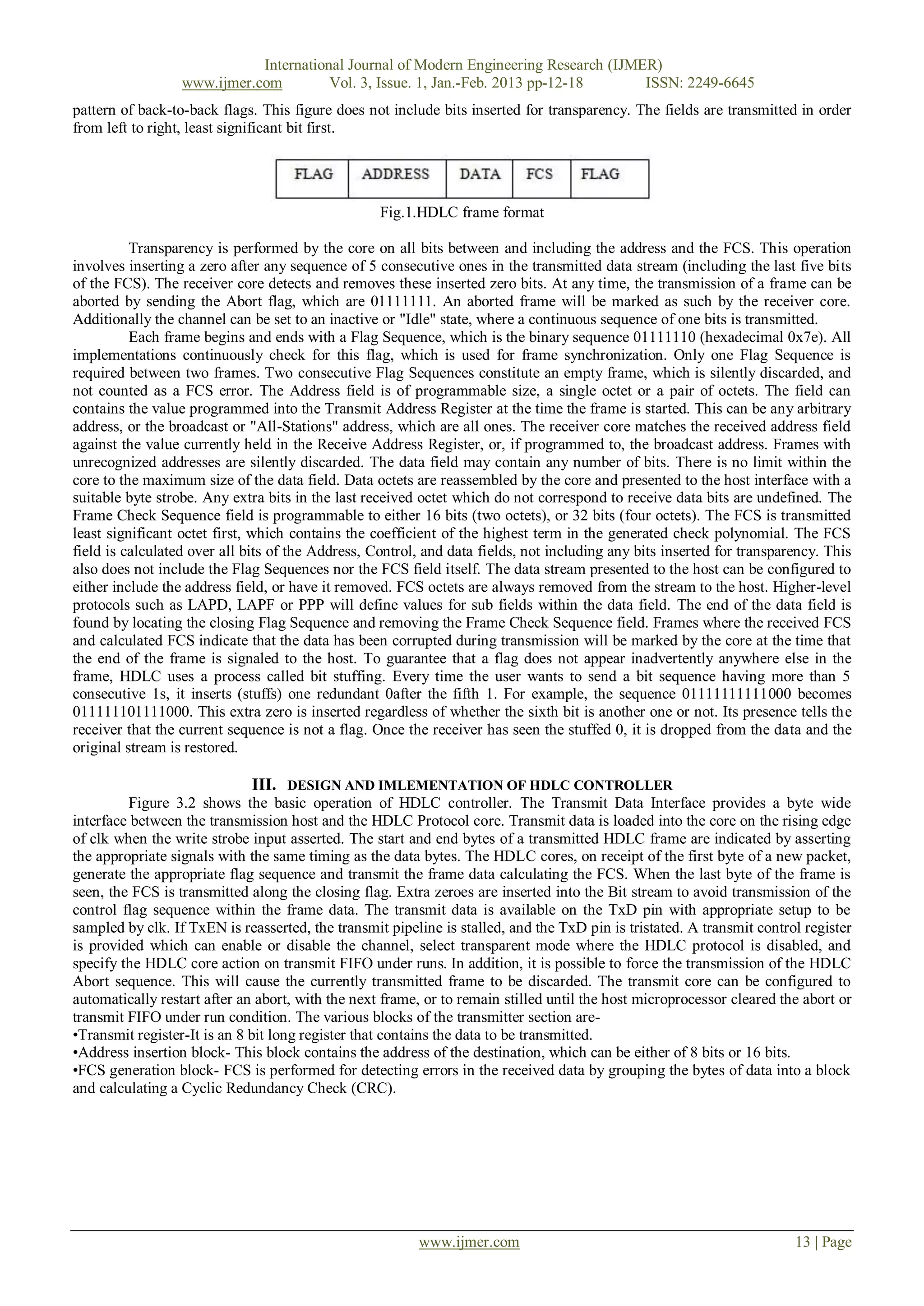
The remainder of this paper is organized as follows: section II describes briefly HDLC frame format. Section III
discusses the system of implemented HDLC controller. Implementation of system on Virtex target is described in section IV.
A comparison of the proposed HDLC controller with some well-known HDLC controllers is presented in section V.
II. SYSTEM MODEL FOR HDLC PROTOCOL
The CDAC HDLC Protocol Core is a high performance module for the bit oriented packet transmission mode. It is
suitable for Frame- Relay; X.25, ISDN B-Channel and D-channel. The core fulfills the specification According to ITU
Q.921, X.25 Level 2 recommendation. The data interface is 8 bit wide synchronous and is suitable for interfacing to transmit
and receive FIFOs.An example of an HDLC frame structure is shown below, for an 8-bit address field with an interframe fill
www.ijmer.com 12 | Page](https://image.slidesharecdn.com/ac311218-130215013331-phpapp02/75/Design-and-Implementation-of-HDLC-Controller-by-Using-Crc-16-1-2048.jpg)
![International Journal of Modern Engineering Research (IJMER)
www.ijmer.com Vol. 3, Issue. 1, Jan.-Feb. 2013 pp-12-18 ISSN: 2249-6645
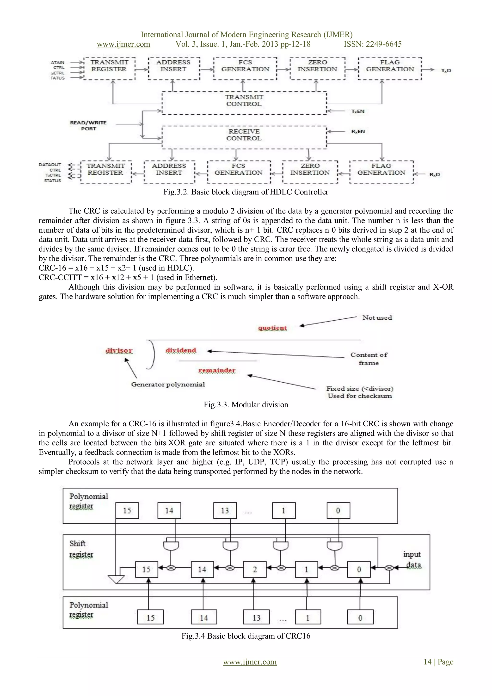
• Zero insertion block- A bit sequence having more than 5 consecutive 1s, this block inserts (stuffs) one redundant 0after
the fifth 1.
• Flag generation block- To inform the receiving station that a new packet is arriving; a specific bit pattern 01111110 is
affixed in the beginning.
• Transmit control register- This register controls the flow of data from transmitter to receiver.
Receiver section-The HDLC protocol core receiver accepts a bit stream. The flag detection block searches the bit
stream for the flag sequence in order to determine the frame boundaries. Any stuffed zeroes are detected and removed by the
zero deletion blocks and the FCS is calculated and checked by the FCS-16 or FCS-32 block depending on the control register
word. The bit stream is accepted on port RxD. The data is latched on the rising edge of clk under the control of the enable
input RxEN. The flag detection block stream for the flag sequence in order to determine the frame boundaries. Any stuffed
zeroes are detected and removed and the FCS is calculated and checked. Frame data is placed on the receiver data interface
and made available to the host. In addition, flag information is passed over indicating the start and end bytes of the HDLC
frame as well as showing any error condition which may have been detected during receipt of the frame.
The receiver can be configured into transparent mode, effectively disabling the HDLC protocol functions. In normal
HDLC protocol made, all received frames are presented to the host on the output register[6]. A status register is provided
which can be used to monitor the status of the receiver channel, and indicates if the packet currently being received includes
any errors. The various blocks in this section are:
• Flag detection block- It checks for the incoming flag.
• Zero deletion block- This block deletes the stuffed zeroes which were introduced during transmission.
• FCS calculator- Calculate the FCS and if the remainder comes out be zero that represents error free transmission.
This block performs the reverse function of the FCS generator. The whole packet is again divided by the same
polynomial that was used at the transmitter end i.e.
CRC-16 = x16 + x15 + x2+ 1
CRC-32 = x32 + x26 + x23 + x22 + x16 + x12 + x11 + x10 + x8 + x7 + x5 + x4 + x2 + x + 1
Fig.3.5 Basic block diagram of CRC16
If after the packet with the polynomial the remainder comes out to be zero that means the transmission and
reception are error free and in case the remainder is not zero that means an error has occurred during the process and hence
the packet is discarded and the whole packet is retransmitted.
1. Data unit arrives at the receiver data first, followed by CRC. The receiver treats the whole string as a data unit and divides
by the same divisor.
2. If remainder comes out to be 0 the string is error free and is accepted but if the remainder comes out to be other than 0, it
is assumed that it contains an error and the whole frame is discarded and is retransmitted.
• Address detector- It detects the address and matched with the address of the destination.
• Receive register- It contains the original 8 bit data sent by the receiver.
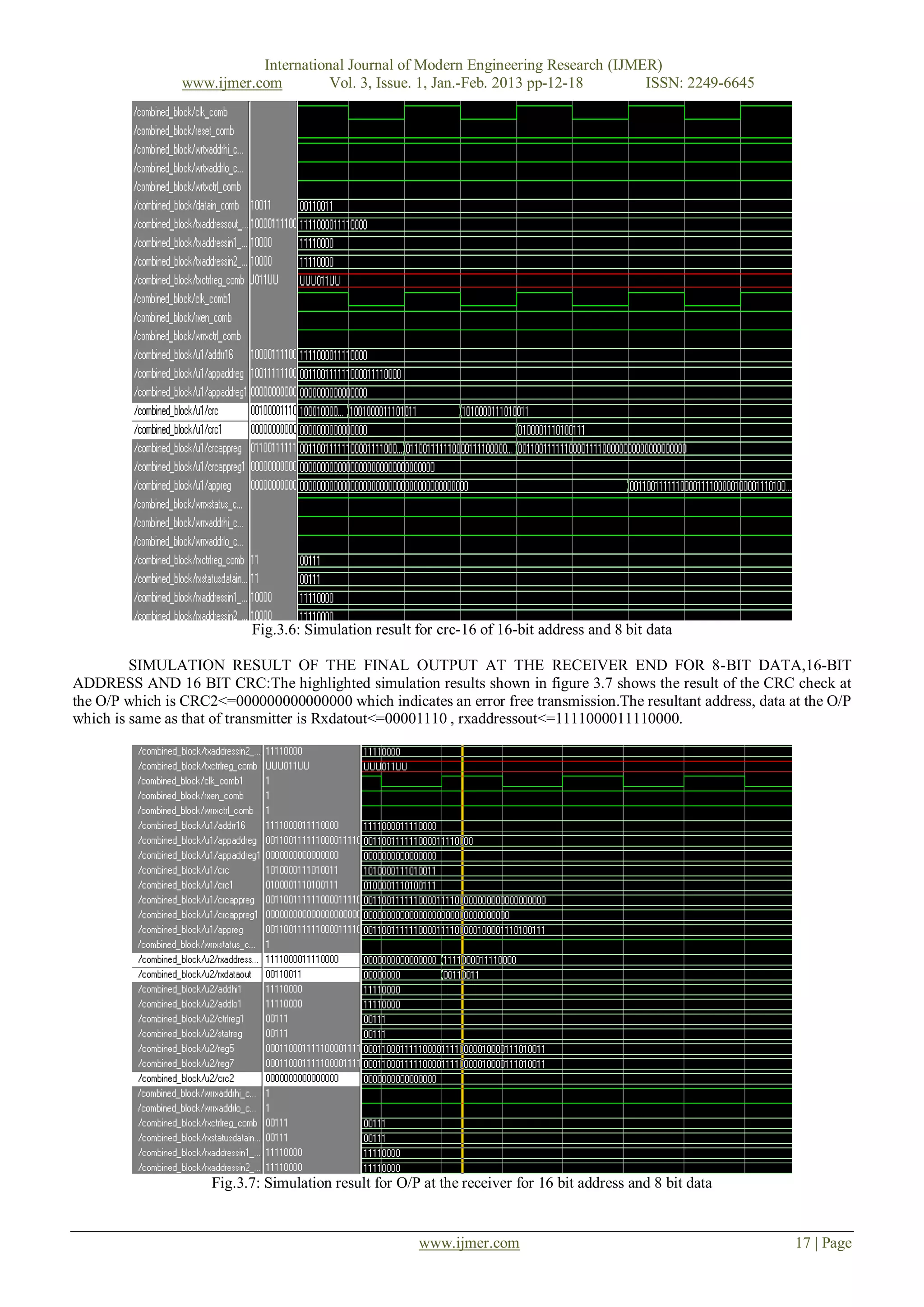
IV. SIMULATION RESULTS
The design and implementation of the HDLC Controller, the results obtained are as follows:
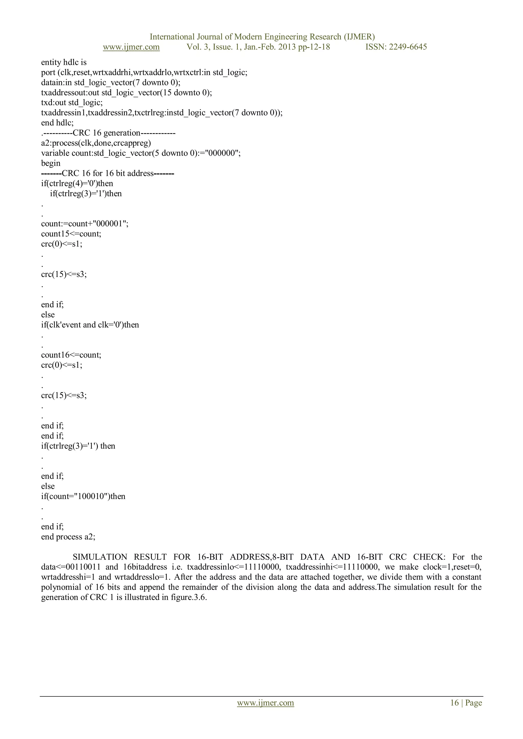
VHDL CODE FOR HDLC Controller
Title:HDLC components package for HDLC controller
File:hdlc_components_pkg.vhd
Simulators:Modelsim 5.3XE/Windows98
Dependency: ieee.std_logic_1164
--------- CODE FOR CRC-16 GENERATION ------------
Library IEEE;
Use IEEE.STD_LOGIC_1164.ALL;
Use IEEE.STD_LOGIC_ARITH.ALL;
Use IEEE.STD_LOGIC_UNSIGNED.ALL;
Uncomment the following library declaration if instantiating any Xilinx primitives in this code.
--library UNISIM;
--use UNISIM.VComponents.all;
www.ijmer.com 15 | Page](https://image.slidesharecdn.com/ac311218-130215013331-phpapp02/75/Design-and-Implementation-of-HDLC-Controller-by-Using-Crc-16-4-2048.jpg)
![International Journal of Modern Engineering Research (IJMER)
www.ijmer.com Vol. 3, Issue. 1, Jan.-Feb. 2013 pp-12-18 ISSN: 2249-6645
V. CONCLUSION
In this paper, we have studied and simulated the HDLC Controller of 16-bit address for 8-bit data. It can
automatically check the frame sequence generation by every time the user want to send a bit sequence using cyclic
redundancy check CRC-16 to provide error free transmission of data.The simulation result of Post Synthesis is an Optimized
Gate Level net list form which a net list code is extracted and it is simulated using Simulator and it is verified that design is
working efficiently. In this paper,we studied and implemented the HDLC and CRC Calculation. The aim of this paper is to
run the programmed FPGA at frequency i.e. in our simulation result,with single +5 V power supply, it performs up to
155.52 Mbits/s data rates.furthermore,we implemented the various HDLC controllers for 16-bit address, 8 bit data and 16 bit
CRC Check, simulation result for final output at the receiver end for 8-bit data16-bit address and 16-bit CRC ,with bit
stuffing and removal of error in HDLC.it is capable of working in different modes:Normal response mode,asynchronous
response mode and asynchronous balanced mode.HDLC controller desgn supports full Duplex and half duplex mode of
operations.It is CCITT X.25 compatible, which is a protocol at the physical layer.An Automation Frame Check Sequence
(CRC) generation at the transmitter end and it is capable of checking the receiver end for reliable and error free
transmission.Also flexible with minimum CPU Overhead as it supports a comprehensive frame Level instruction set.It is
Fully Compatible with TTL ICs.
REFERENCES
[1] Gaurav Chandil;Priyanka Mishra;”Study and performance evaluation of Xilinx HDLC Controller and FCS Calculator”,vol.2,issue
10 (October 2012),PP 41-50.
[2] William Stallings, 2007. Data and Computer Communications, Eight edition, Prentice Hall, pp: 222.
[3] Amit Dhir, 2000. “HDLC Controller Solutions with Spartan-II FPGAs,” Xilinx Inc.
[4] M.A.; Barbetta, L.; Neri, F.; “A Petri net simulation model of HDLC Marsan”,TENCON '89. Fourth IEEE Region 10 International
Conference 22-24 Nov. 1989Page(s):240–247Digital Object Identifier 0.1109/TENCON.1989.176933.
[5] Davis, G.T.; Mandalia, B.D. “Modified byte insertion/deletion for HDLC in ISDN”;Southeastcon '89. Proceedings 'Energy and
Information Technologies in the Southeast’. IEEE 9-12 April 1989 Page(s):1207 - 1210 vol.3 Digital Object Identifier
10.1109/SECON.1989.132614.
[6] “FPGA implementation of a single-channel HDLC Layer-2 protocol transmitter using VHDL”,Qasim, S.M.; Abbasi, S.A.;
Microelectronics, 2003. ICM 2003. Proceedings of the 15th International Conference on 9-11.
[7] Lu, Y., Z. Wang, L. Qiao and B. Huanq, 2002. "Design and implementation of multi-channel high speed HDLC data processor,"
IEEE International Conference on Communications, Circuits and Systems, and West Sino Expositions, 2: 1471-1475.
[8] Latombe, J. (1996). Robot Motion Planning. Kluwer Academic Publishers, UK.
[9] Jun Wang; Wenhao Zhang; Yuxi Zhang; Wei Wu; Weiguang Chang; Sch. of Electron. & Inf. Eng., Beihang Univ. (BUAA), Beijing,
China “Design and implementation of HDLC procedure based on FPGA” , Anti- ounterfeiting, Security, and Identification in
Communication, 2009. ASID 2009. 3rd International Conference, 20-22 Aug.2009.
[10] Guozheng Li Nanlin Tan State Key Lab. of Rail Traffic Control & Safety, Beijing Jiaotong Univ.,Beijing, China “Design and
Implementation of HDLC Protocol and Manchester Encoding Based on FPGA in Train Communication Network”, Information and
Computing (ICIC), 2010 Third International Conference.
[11] Allaire, F.C.J., M. Tarbouchi, G. Labonte and G. Fusina, 2009. "FPGA implementation of genetic algorithm for UAV real-time path
planning," Journal of Intelligent and Robotic Systems: Theory and Applications, 54(1-3): 495-510.
[12] Chen, H. and Y.Q. Han, 2003. "ASIC design of high-speed low-power HDLC controller," Journal of Beijing Institute of Technology
(English Edition), 12(SUPPL.): 66-69.
[13] Gao, Zhen-bin and Jian-Fei Liu, 2005. "FPGA implementation of a multi-channel HDLC protocol transceiver", In Proceedings of
the 2005 International Conference on Communications, Circuits and Systems,2: 1300-1302.
www.ijmer.com 18 | Page](https://image.slidesharecdn.com/ac311218-130215013331-phpapp02/75/Design-and-Implementation-of-HDLC-Controller-by-Using-Crc-16-7-2048.jpg)

This document summarizes a research paper that designed, simulated, and implemented an HDLC controller using VHDL on a Spartan 3 FPGA. The HDLC controller supports data transmission rates up to 155.52 Mbps and complies with ITU and X.25 standards. It allows synchronous, transparent data transmission over point-to-point and multipoint channels. The design was tested through simulation and synthesis, and implemented CRC-16, bit stuffing/removal and error detection. The goal was to efficiently utilize FPGA resources to run the programmed design at high speeds.