Downloaded 47 times


![Some important equations in the
inversion regime (Depth direction)
VT = φms + 2ψB + ψox
Wdm = √[2εS(2ψB)/qNA]
Qinv = Cox(VG - VT)
ψox = Qs/Cox
Qs = qNAWdm
VT = φms + 2ψB + (√[4εSψBqNA] - Qf + Qm + Qot)/Cox
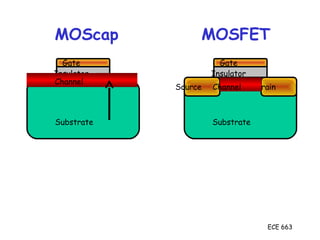
Substrate
Channel Drain
Insulator
Gate
Source
x](https://image.slidesharecdn.com/mos-130626204655-phpapp01/85/Mos-8-320.jpg)


![Simplified MOSFET I-V
Equations
Cut-off: VGS< VT
ID = IS = 0
Active: VGS>VT and VDS < VGS-VT
ID = kn
’
(W/L)[(VGS-VT)VDS - 1
/2VDS
2
]
Saturation: VGS>VT and VDS > VGS-VT
ID = 1
/2kn’(W/L)(VGS-VT)2](https://image.slidesharecdn.com/mos-130626204655-phpapp01/85/Mos-14-320.jpg)

This document discusses the operation and key characteristics of metal-oxide-semiconductor (MOS) devices including MOS diodes and MOS field-effect transistors (MOSFETs). It describes the different operating regions of MOS diodes such as accumulation, depletion, and inversion based on the applied gate voltage. It also explains how a MOSFET operates as a switching device when a positive gate voltage is applied for n-type operation. Important equations for threshold voltage, pinch-off effect, and current-voltage relationships in different operating regions are provided.


