How to include y-dependent potential without doing the whole problem over?
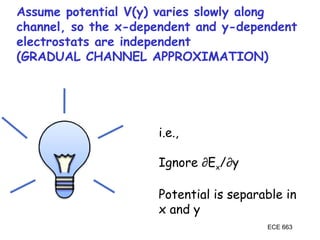
Assume potential V(y) varies slowly along channel, so the x-dependent and y-dependent electrostats are independent �(GRADUAL CHANNEL APPROXIMATION)
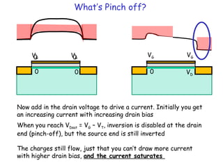
When you reach VDsat = VG – VT, inversion is disabled at the drain end (pinch-off), but the source end is still inverted
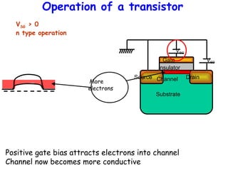
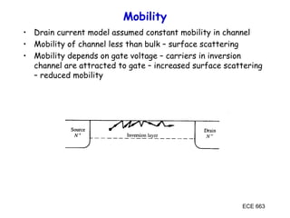
![Some important equations in the
inversion regime (Depth direction)
VT = ms + 2B + ox
Wdm = [2S(2B)/qNA]
Qinv = -Cox(VG - VT)
ox = Qs/Cox
Qs = qNAWdm
VT = ms + 2B + [4SBqNA]/Cox
Substrate
Channel Drain
Insulator
Gate
Source
x](https://image.slidesharecdn.com/lec17mosfetiv-250315163625-19a8ebb7/85/METAL-OXIDE-FIELD-EFFECT-SEMICONDUCTOR-MOSFET-3-320.jpg)
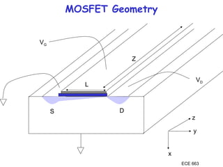
![ECE 663
How to include y-dependent potentials?
S = 2B + V(y)
VG = S + [2SSqNA]/Cox
Need VG – V(y) > VT to invert
channel at y (V increases
threshold)
Since V(y) largest at drain end, that
end reverts from inversion to
depletion first (Pinch off)
SATURATION [VDSAT = VG – VT]](https://image.slidesharecdn.com/lec17mosfetiv-250315163625-19a8ebb7/85/METAL-OXIDE-FIELD-EFFECT-SEMICONDUCTOR-MOSFET-7-320.jpg)
![j = qninvv = (Qinv/tinv)v
I = jA = jZtinv = ZQinvv
ECE 663
So current:
Qinv = -Cox[VG – VT - V(y)]
v = -effdV(y)/dy](https://image.slidesharecdn.com/lec17mosfetiv-250315163625-19a8ebb7/85/METAL-OXIDE-FIELD-EFFECT-SEMICONDUCTOR-MOSFET-8-320.jpg)
![ECE 663
So current:
I = eff ZCox[VG – VT - V(y)]dV(y)/dy
I = eff ZCox[(VG – VT )VD- VD
2
/2]/L
Continuity implies ∫Idy = IL](https://image.slidesharecdn.com/lec17mosfetiv-250315163625-19a8ebb7/85/METAL-OXIDE-FIELD-EFFECT-SEMICONDUCTOR-MOSFET-9-320.jpg)
![ECE 663
But this current behaves like a parabola !!
ID
VD
IDsat
VDsat
I = eff ZCox[(VG – VT )VD- VD
2
/2]/L
We have assumed inversion in our model (ie, always above pinch-off)
So we just extend the maximum current into saturation…
Easy to check that above current is maximum for VDsat = VG - VT
Substituting, IDsat = (CoxeffZ/2L)(VG-VT)2](https://image.slidesharecdn.com/lec17mosfetiv-250315163625-19a8ebb7/85/METAL-OXIDE-FIELD-EFFECT-SEMICONDUCTOR-MOSFET-10-320.jpg)
![Square law theory of MOSFETs
I = eff ZCox[(VG – VT )VD- VD
2
/2]/L, VD < VG - VT
I = eff ZCox(VG – VT )2
/2L, VD > VG - VT
J = qnv
n ~ Cox(VG – VT )
v ~ effVD /L
NEW](https://image.slidesharecdn.com/lec17mosfetiv-250315163625-19a8ebb7/85/METAL-OXIDE-FIELD-EFFECT-SEMICONDUCTOR-MOSFET-12-320.jpg)
![ECE 663
BJT vs MOSFET
• RTL logic vs CMOS logic
• DC Input impedance of MOSFET (at gate end) is infinite
Thus, current output can drive many inputs FANOUT
• CMOS static dissipation is low!! ~ IOFFVDD
• Normally BJTs have higher transconductance/current (faster!)
IC = (qni
2
Dn/WBND)exp(qVBE/kT) ID = CoxW(VG-VT) 2
/L
gm = IC/VBE = IC/(kT/q) gm = ID/VG = ID/[(VG-VT)/2]
• Today’s MOSFET ID >> IC due to near ballistic operation
NEW](https://image.slidesharecdn.com/lec17mosfetiv-250315163625-19a8ebb7/85/METAL-OXIDE-FIELD-EFFECT-SEMICONDUCTOR-MOSFET-32-320.jpg)
![ECE 663
It also affects the I-V
VG
The threshold voltage is increased due to the depletion region
that grows at the drain end because the inversion layer shrinks
there and can’t screen it any more. (Wd > Wdm)
Qinv = -Cox[VG-VT(y)], I = -effZQinvdV(y)/dy
VT(y) = + √2sqNA/Cox
= 2B + V(y)](https://image.slidesharecdn.com/lec17mosfetiv-250315163625-19a8ebb7/85/METAL-OXIDE-FIELD-EFFECT-SEMICONDUCTOR-MOSFET-36-320.jpg)
![ECE 663
It also affects the I-V
IL = ∫effZCox[VG – (2B+V) - √2sqNA(2B+V)/Cox]dV
I = (ZeffCox/L)[(VG–2B)VD –VD
2
/2
-2√2sqNA{(2B+VD)3/2
-(2B)3/2
}/3Cox]](https://image.slidesharecdn.com/lec17mosfetiv-250315163625-19a8ebb7/85/METAL-OXIDE-FIELD-EFFECT-SEMICONDUCTOR-MOSFET-37-320.jpg)
![ECE 663
We can approximately include this…
Include an additional charge term from the
depletion layer capacitance controlling V(y)
Q = -Cox[VG-VT]+(Cox + Cd)V(y)
where Cd = s/Wdm
Q = -Cox[VG –VT - MV(y)], M = 1 + Cd/Cox
ID = (ZeffCox/L)[(VG-VT - MVD/2)VD]](https://image.slidesharecdn.com/lec17mosfetiv-250315163625-19a8ebb7/85/METAL-OXIDE-FIELD-EFFECT-SEMICONDUCTOR-MOSFET-38-320.jpg)