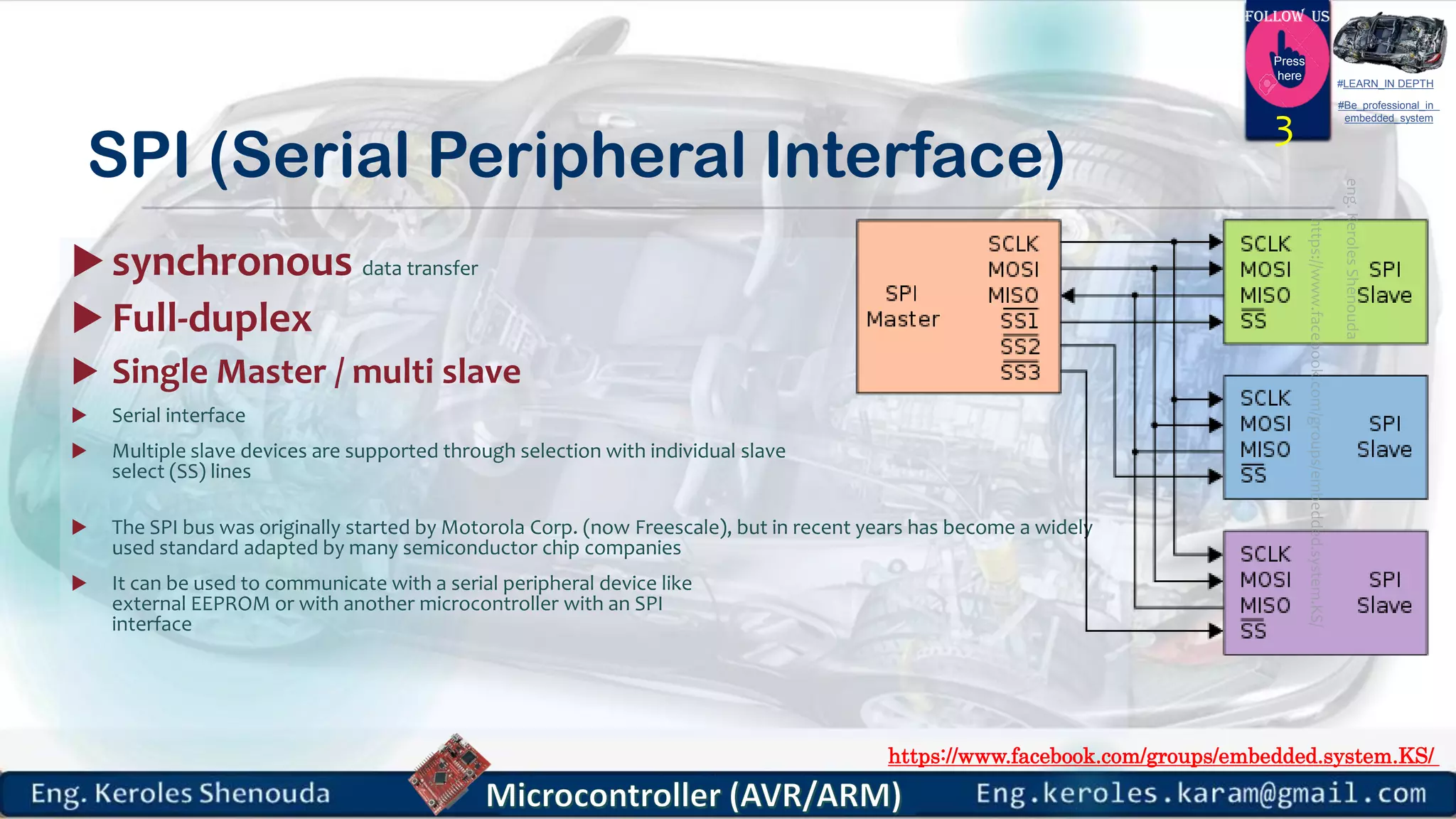
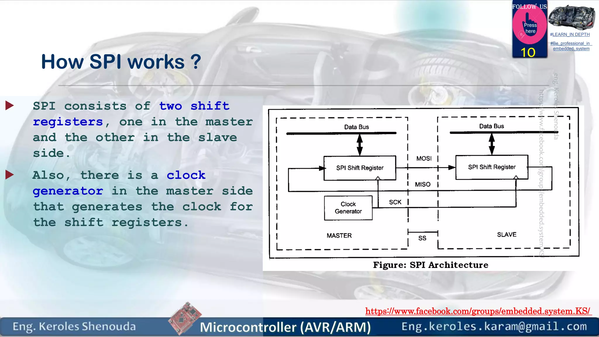
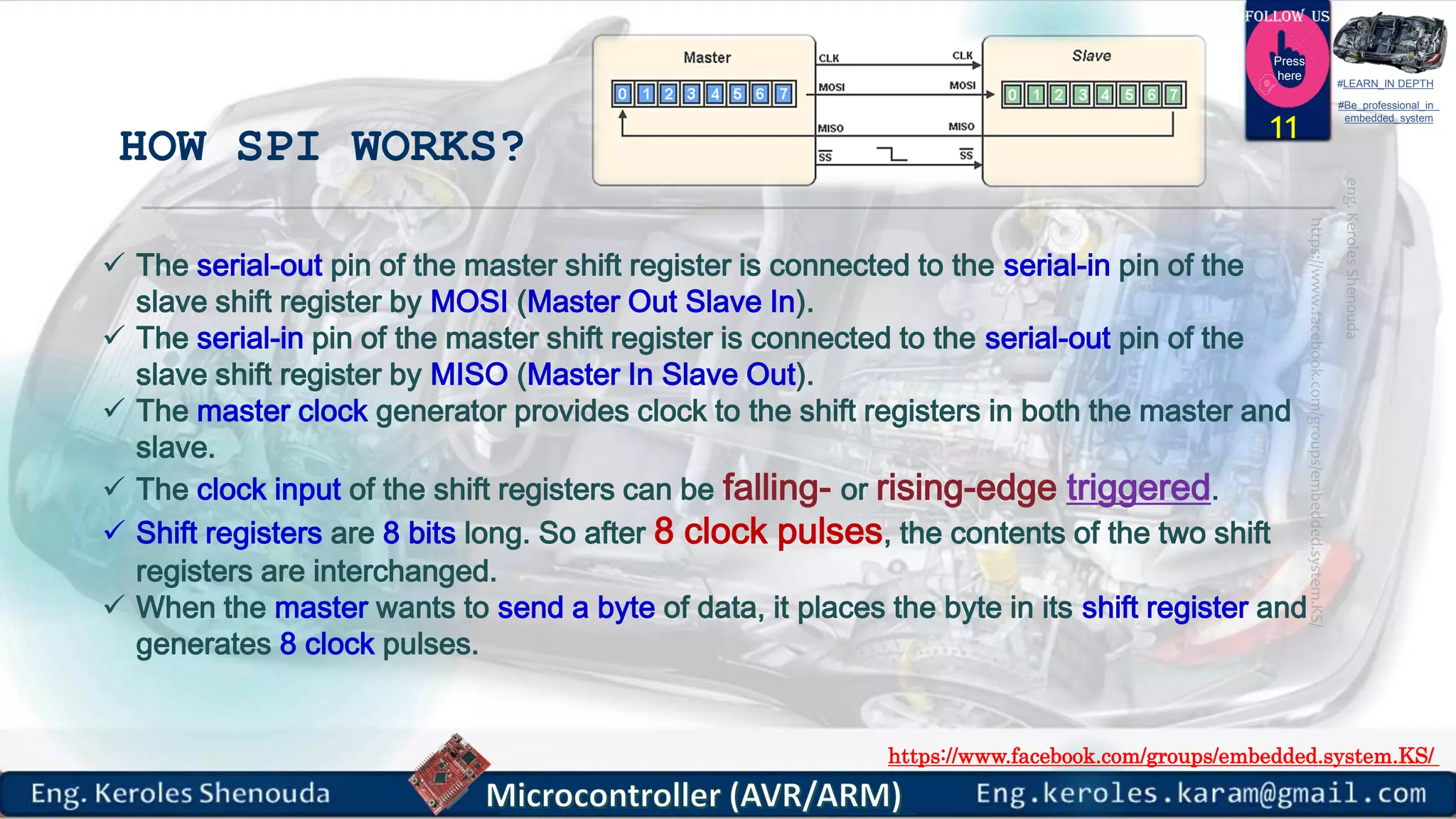
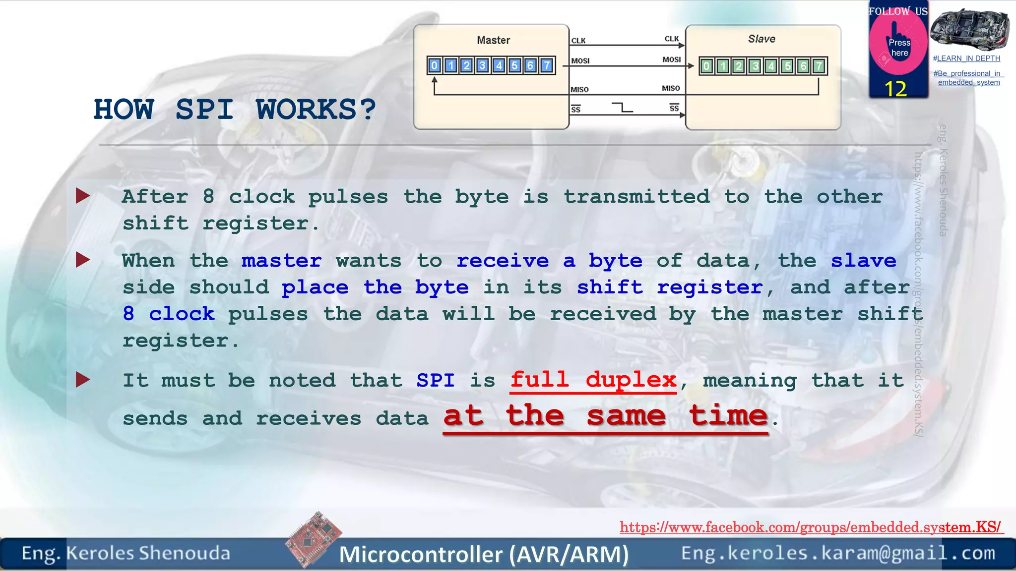
1) SPI (Serial Peripheral Interface) is a synchronous serial communication interface standard used for communicating with serial peripheral devices.
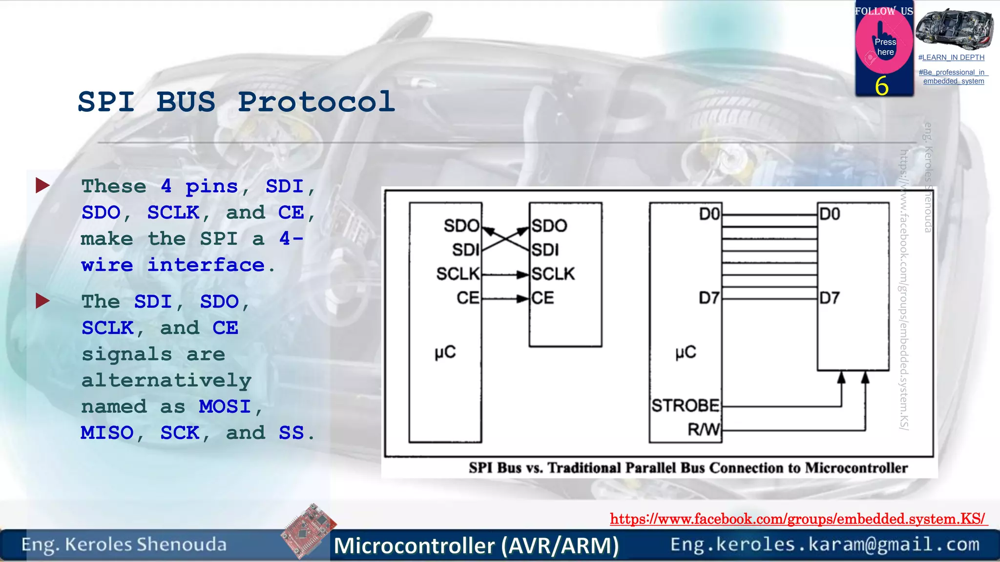
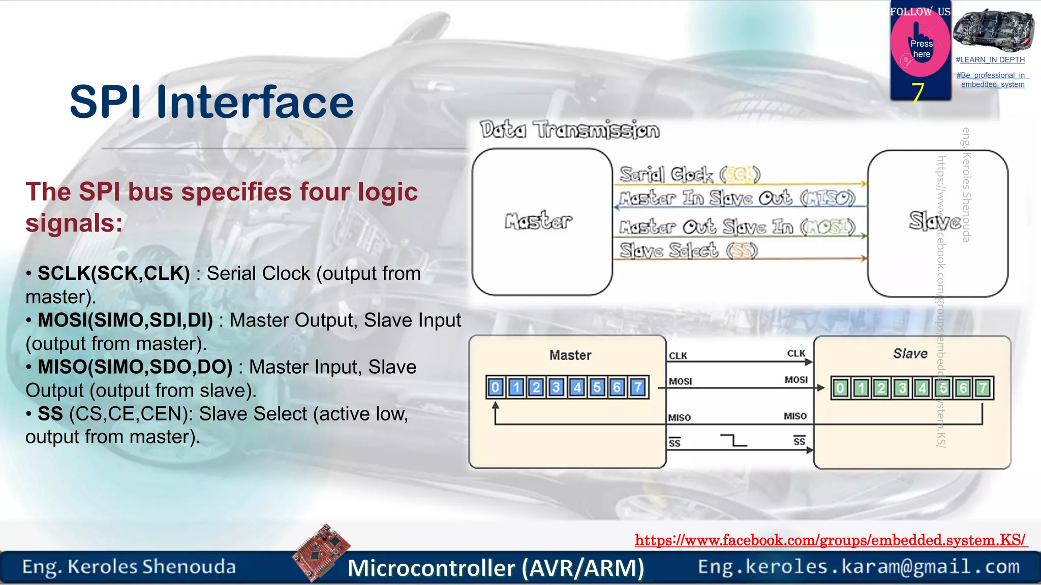
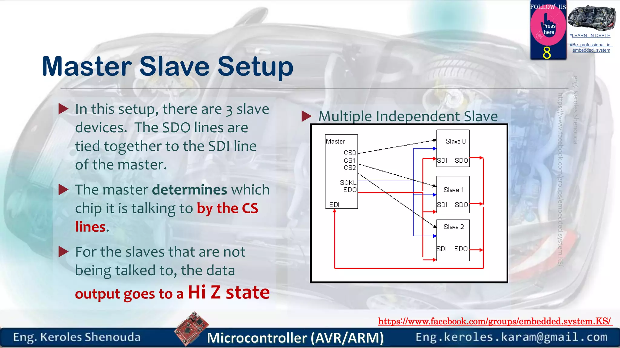
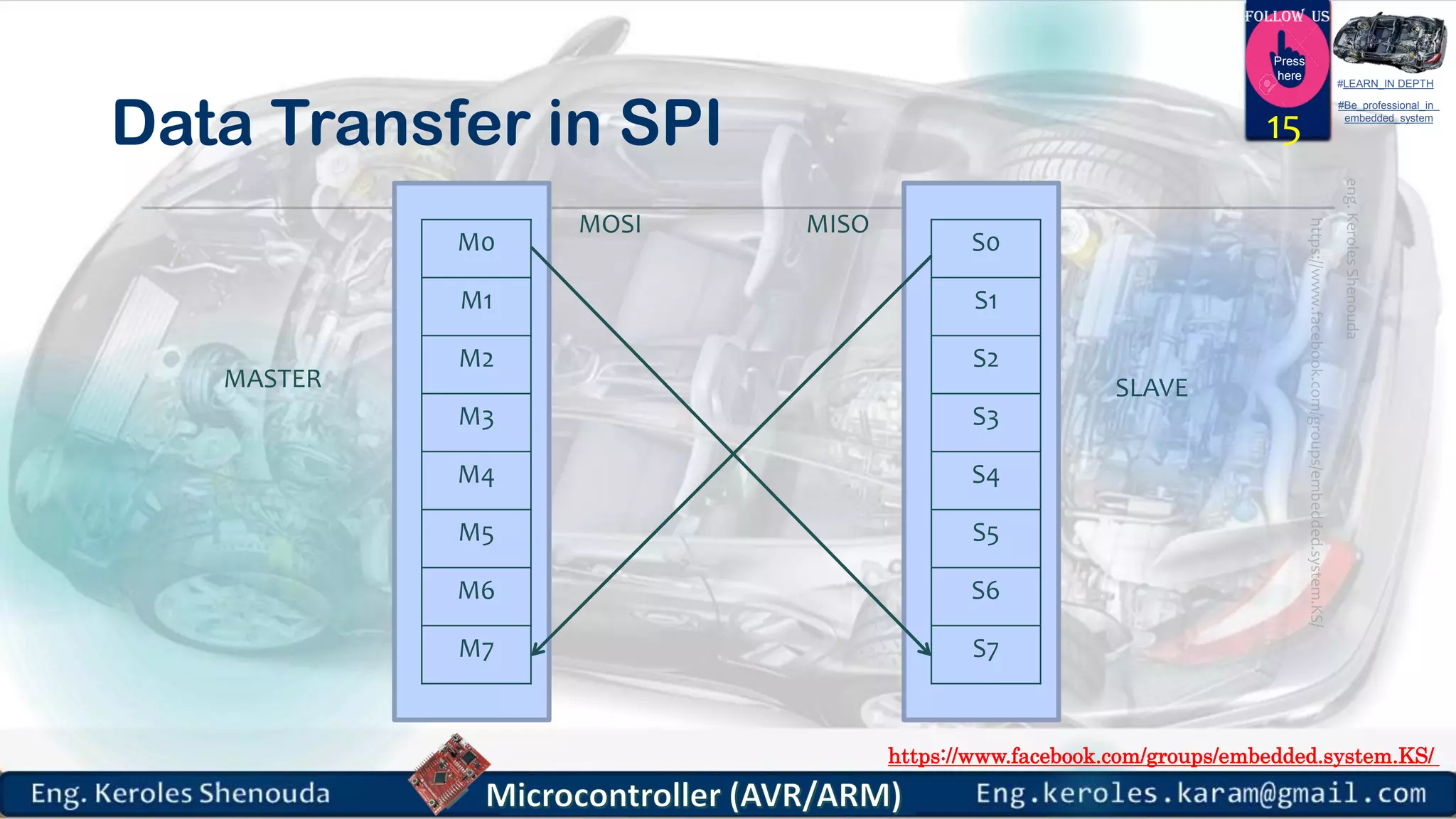
2) SPI uses four signals - Serial Clock (SCLK), Master Output Slave Input (MOSI), Master Input Slave Output (MISO), and Slave Select (SS). It can support multiple slaves through individual SS lines.
3) SPI is full duplex, allowing simultaneous transmission and reception of data. It provides higher throughput than I2C but requires more pins and the master must control all communication.


![https://www.facebook.com/groups/embedded.system.KS/
Follow us
Press
here
#LEARN_IN DEPTH
#Be_professional_in
embedded_system
QUAD SPI [QSPI]
28](https://image.slidesharecdn.com/microcontrollerpart8v1-171015135321/75/Microcontroller-part-8_v1-28-2048.jpg)
![https://www.facebook.com/groups/embedded.system.KS/
Follow us
Press
here
#LEARN_IN DEPTH
#Be_professional_in
embedded_system
QUAD SPI [QSPI]
Multi I/O variants such as dual I/O and quad
I/O add additional data lines to the standard
for increased throughput. This
performance increase enables random
access and direct program execution from
flash memory (execute-in-place)
A multi I/O SPI device is capable of
supporting increased bandwidth or
throughput from a single device. A dual
I/O (two-bit data bus) interface enables
transfer rates to double compared to the
standard serial Flash memory devices.
A quad I/O (four-bit data bus) interface
improves throughput four times.
29](https://image.slidesharecdn.com/microcontrollerpart8v1-171015135321/75/Microcontroller-part-8_v1-29-2048.jpg)


![https://www.facebook.com/groups/embedded.system.KS/
Follow us
Press
here
#LEARN_IN DEPTH
#Be_professional_in
embedded_system
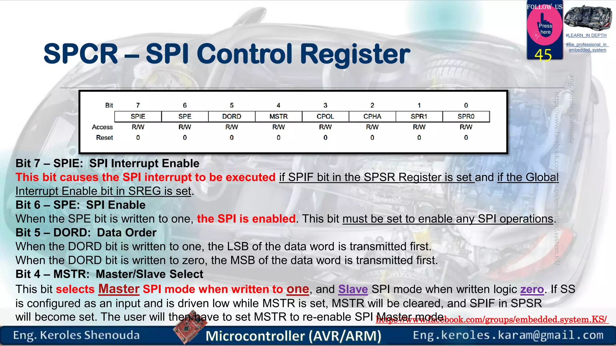
SPCR – SPI Control Register
Bits 1:0 – SPRn: SPI Clock Rate Select [n = 1:0]
47](https://image.slidesharecdn.com/microcontrollerpart8v1-171015135321/75/Microcontroller-part-8_v1-47-2048.jpg)


![https://www.facebook.com/groups/embedded.system.KS/
Follow us
Press
here
#LEARN_IN DEPTH
#Be_professional_in
embedded_system
Lab1 : transmit a
character between
two ATmega32
microcontrollers
[Solution] (Master)
70](https://image.slidesharecdn.com/microcontrollerpart8v1-171015135321/75/Microcontroller-part-8_v1-70-2048.jpg)
![https://www.facebook.com/groups/embedded.system.KS/
Follow us
Press
here
#LEARN_IN DEPTH
#Be_professional_in
embedded_system
Lab1 : transmit a
character between
two ATmega32
microcontrollers
[Solution] (Slave)
71](https://image.slidesharecdn.com/microcontrollerpart8v1-171015135321/75/Microcontroller-part-8_v1-71-2048.jpg)