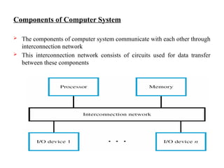
Components of ComputerSystem
The components of computer system communicate with each other through
interconnection network
This interconnection network consists of circuits used for data transfer
between these components
4.
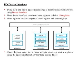
I/O Device Interface
Every input and output device is connected to the interconnection network
using Device Interface
These device interfaces consists of some registers called as I/O registers
These registers are: Data register, Control register and Status register
Above diagram shows the presence of data, status and control registers
inside the device interface of keyboard and display device
5.
Data Transfer betweenI/O device and Computer
The data transfer between I/O devices and the processor can be carried out
in 2 ways:
1. Program-Controlled I/O
2. Interrupt driven I/O
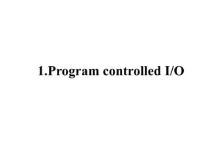
1.Program controlled I/O
Writing the set of instructions for performing data transfer between CPU
and I/O device is called Program controlled I/O
Here while reading data from input device for example keyboard,
whenever user has pressed a character, it will be stored in the Data register
of the keyboard and the KIN flag in the Status register will be set to 1 (see
diagram in next slide)
Similarly during writing of data to output device for example display
device, whenever the output device is ready, it sets the DOUT flag in
Status register to 1. CPU before sending data to display device checks the
DOUT flag in status register first. If it is 1 then only CPU sends the data
which gets stored in Data register of display device. From there display
device takes the data and display in the screen(see diagram in next slide)
8.
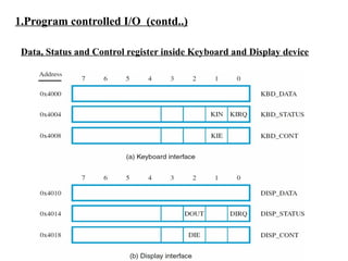
1.Program controlled I/O(contd..)
Data, Status and Control register inside Keyboard and Display device
9.
1.Program controlled I/O(contd..)
In the diagram in previous slide,
KDB_DATA – Keyboard Data register
KDB_STATUS – Keyboard Status register
KDB_ CONT – Keyboard Control register
DISP_DATA – Display device Data register
DISP_STATUS – Display device Status register
DISP_CONT – Display device Control register
Every register is of 8 bits in size and has a memory address. Through that
memory address only CPU will communicate with that device
KIN flag is present in the 1st
bit position in status register of keyboard and
DOUT flag is present in the 2nd
bit position in status register of display
device
10.
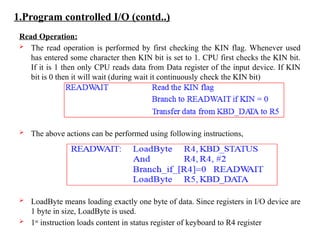
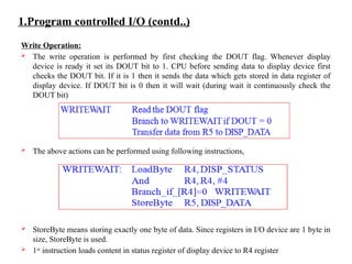
1.Program controlled I/O(contd..)
Read Operation:
The read operation is performed by first checking the KIN flag. Whenever used
has entered some character then KIN bit is set to 1. CPU first checks the KIN bit.
If it is 1 then only CPU reads data from Data register of the input device. If KIN
bit is 0 then it will wait (during wait it continuously check the KIN bit)
The above actions can be performed using following instructions,
LoadByte means loading exactly one byte of data. Since registers in I/O device are
1 byte in size, LoadByte is used.
1st
instruction loads content in status register of keyboard to R4 register
11.
1.Program controlled I/O(contd..)
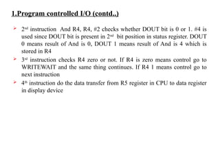
2nd
instruction And R4, R4, #2 checks whether KIN bit is 0 or 1. #2 is used
since KIN bit is present in 1st
bit position in status register. KIN 0 means
result of And is 0, KIN 1 means result of And is 2 which is stored in R4
3rd
instruction checks R4 zero or not. If R4 is zero means control go to
READWAIT and the same thing continues. If R4 1 means control go to
next instruction
4th
instruction do the data transfer from data register in keyboard to R5
register in keyboard
12.
1.Program controlled I/O(contd..)
Write Operation:
The write operation is performed by first checking the DOUT flag. Whenever display
device is ready it set its DOUT bit to 1. CPU before sending data to display device first
checks the DOUT bit. If it is 1 then it sends the data which gets stored in data register of
display device. If DOUT bit is 0 then it will wait (during wait it continuously check the
DOUT bit)
The above actions can be performed using following instructions,
StoreByte means storing exactly one byte of data. Since registers in I/O device are 1 byte in
size, StoreByte is used.
1st
instruction loads content in status register of display device to R4 register
13.
1.Program controlled I/O(contd..)
2nd
instruction And R4, R4, #2 checks whether DOUT bit is 0 or 1. #4 is
used since DOUT bit is present in 2nd
bit position in status register. DOUT
0 means result of And is 0, DOUT 1 means result of And is 4 which is
stored in R4
3rd
instruction checks R4 zero or not. If R4 is zero means control go to
WRITEWAIT and the same thing continues. If R4 1 means control go to
next instruction
4th
instruction do the data transfer from R5 register in CPU to data register
in display device
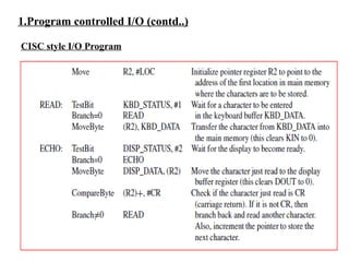
1.Program controlled I/O(contd..)
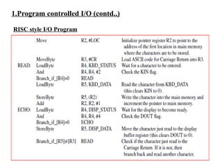
RISC style I/O Program
Instructions in previous slide read data from keyboard and stores it in R5
register. From there it is saved in the memory and also data is displayed in
the display device.
The above one continues until user entered the Carriage Return(CR)
character. The CR character indicates the last character
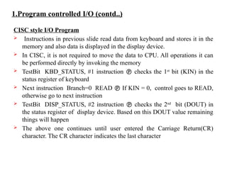
1.Program controlled I/O(contd..)
CISC style I/O Program
Instructions in previous slide read data from keyboard and stores it in the
memory and also data is displayed in the display device.
In CISC, it is not required to move the data to CPU. All operations it can
be performed directly by invoking the memory
TestBit KBD_STATUS, #1 instruction checks the 1st
bit (KIN) in the
status register of keyboard
Next instruction Branch=0 READ If KIN = 0, control goes to READ,
otherwise go to next instruction
TestBit DISP_STATUS, #2 instruction checks the 2nd
bit (DOUT) in
the status register of display device. Based on this DOUT value remaining
things will happen
The above one continues until user entered the Carriage Return(CR)
character. The CR character indicates the last character
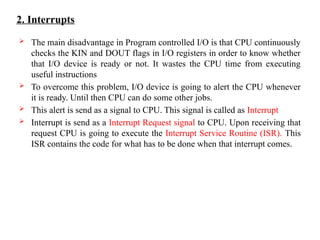
2. Interrupts
Themain disadvantage in Program controlled I/O is that CPU continuously
checks the KIN and DOUT flags in I/O registers in order to know whether
that I/O device is ready or not. It wastes the CPU time from executing
useful instructions
To overcome this problem, I/O device is going to alert the CPU whenever
it is ready. Until then CPU can do some other jobs.
This alert is send as a signal to CPU. This signal is called as Interrupt
Interrupt is send as a Interrupt Request signal to CPU. Upon receiving that
request CPU is going to execute the Interrupt Service Routine (ISR). This
ISR contains the code for what has to be done when that interrupt comes.
20.
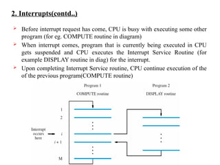
2. Interrupts(contd..)
Beforeinterrupt request has come, CPU is busy with executing some other
program (for eg. COMPUTE routine in diagram)
When interrupt comes, program that is currently being executed in CPU
gets suspended and CPU executes the Interrupt Service Routine (for
example DISPLAY routine in diag) for the interrupt.
Upon completing Interrupt Service routine, CPU continue execution of the
of the previous program(COMPUTE routine)
21.
2. Interrupts(contd..)
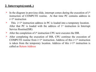
Inthe diagram in previous slide, interrupt comes during the execution of ith
instruction of COMPUTE routine. At that time PC contains address in
i+1th
instruction
This i+1th
instruction address in PC is loaded into a temporary location.
After that PC is loaded with the address of 1st
instruction in Interrupt
Service Routine(ISR)
After the completion of ith
instruction CPU next executes the ISR.
After completing the execution of ISR, CPU continue the execution of
COMPUTE routine from i+1th
instruction. Address of this i+1th
instruction
is taken from the temporary location. Address of this i+1th
instruction is
called as Return Address
22.
2. Interrupts(contd..)
I/Odevice will continue sending its interrupt request signal to CPU until it
know that its request has been recognized by CPU
I/O device will stop sending the interrupt request signal when its knows
that its request has been recognized by the CPU
CPU inform the device that the request has been recognized in 2 ways,
1. CPU can send a control signal called interrupt acknowledge which
indicates that the interrupt request has been recognized by the CPU
2. The execution of ISR which access the data or status register of device
implicitly implies that the request from device has been recognized by the
CPU
23.
2. Interrupts(contd..)
Interrupt Latencyand Shadow Registers
When an interrupt arrives, before executing the ISR, information (like
information in PC, status register and other register contents) related to the
program that is currently been executed by the CPU must be saved
The interval between the time when an interrupt request is arrived and the
start of the execution of the interrupt service routine is called interrupt
latency
In order to reduce the time gap between interrupt arrival time and
executing of its ISR, duplicate registers are used. One set of registers for
executing normal programs and another set of registers for executing ISR.
Duplicate registers are called as Shadow registers
24.
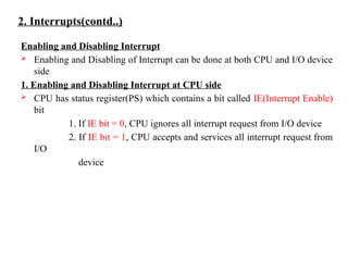
2. Interrupts(contd..)
Enabling andDisabling Interrupt
Enabling and Disabling of Interrupt can be done at both CPU and I/O device
side
1. Enabling and Disabling Interrupt at CPU side
CPU has status register(PS) which contains a bit called IE(Interrupt Enable)
bit
1. If IE bit = 0, CPU ignores all interrupt request from I/O device
2. If IE bit = 1, CPU accepts and services all interrupt request from
I/O
device
25.
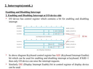
2. Interrupts(contd..)
Enabling andDisabling Interrupt
2. Enabling and Disabling Interrupt at I/O device side
I/O device has control register which contains a bit for enabling and disabling
interrupt
In above diagram Keyboard control register has KIE (Keyboard Interrupt Enable)
bit which can be used for enabling and disabling interrupt at keyboard. If KIE=1
then only I/O device can raise the interrupt requests.
Similarly DIE (Display Interrupt Enable) bit in control register of display device
can be used
IE bit
26.
2. Interrupts(contd..)
Enabling andDisabling Interrupt
The following are the steps during interrupt,
1. The device raises an interrupt request.
2. The processor interrupts the program currently being executed and saves the
contents of the PC and PS registers.
3. Interrupts are disabled by clearing the IE bit in the PS to 0.
4. The action requested by the interrupt is performed by the interrupt-service
routine, during which time the device is informed that its request has been
recognized, and in response, it deactivates the interrupt-request signal.
5. Upon completion of the interrupt-service routine, the saved contents of
the PC and PS registers are restored (enabling interrupts by setting the IE bit
to 1), and execution of the interrupted program is resumed.
27.
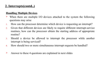
2. Interrupts(contd..)
Handling MultipleDevices
When there are multiple I/O devices attached to the system the following
questions may arise
1. How can the processor determine which device is requesting an interrupt?
2. Given that different devices are likely to require different interrupt-service
routines, how can the processor obtain the starting address of appropriate
routine?
3. Should a device be allowed to interrupt the processor while another
interrupt is being serviced?
4. How should two or more simultaneous interrupt requests be handled?
Answer to these 4 questions are explained in next slides
28.
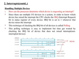
2. Interrupts(contd..)
Handling MultipleDevices
1. How can the processor determine which device is requesting an interrupt?
Since there are multiple I/O devices in a system, in order to know which
device has raised the interrupt the CPU checks the IRQ (Interrupt Request)
bit in status register of every device. IRQ bit is set to 1 whenever that
device raises the interrupt
This technique of checking the IRQ bit of all devices is called Polling
This polling technique is easy to implement but time get wasted by
checking the IRQ bit of device that does not raised interrupt(non-
interrupted device)
IRQ Bit
29.
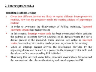
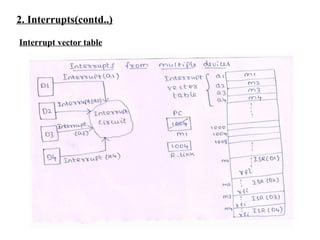
2. Interrupts(contd..)
Handling MultipleDevices
2. Given that different devices are likely to require different interrupt-service
routines, how can the processor obtain the starting address of appropriate
routine?
In order to overcome the disadvantage of Polling technique, Vectored
Interrupts scheme has been proposed
In this scheme, Interrupt vector table has been constructed which contains
the address of Interrupt Service Routines of all devices(where ISR for a
device present in the memory). These address are called as Interrupt
vector. Interrupt service routine can be present anywhere in the memory
When an interrupt request arrives, the information provided by the
requesting device can be used as a pointer to the interrupt vector table and
the address of the corresponding ISR is fetched
Thus using this interrupt vector table, processor knows which device raised
the interrupt and also obtains the starting address of appropriate ISR
2. Interrupts(contd..)
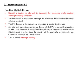
Handling MultipleDevices
3. Should a device be allowed to interrupt the processor while another
interrupt is being serviced?
Yes the device is allowed to interrupt the processor while another interrupt
is being serviced.
The I/O devices in the system are organized in a priority structure.
An interrupt request comes from a device while CPU is currently executing
an ISR. This interrupt is accepted if the priority of the device which raised
this interrupt is higher than the priority of the currently servicing device.
Otherwise interrupt will be discarded
This is called Interrupt Nesting
32.
2. Interrupts(contd..)
Handling MultipleDevices
4. How should two or more simultaneous interrupt requests be handled?
When multiple devices send the interrupt request at the same time, anyone
of the following approach is used,
1. Polling technique is used in which the device status register is checked
based in a priority manner
2. Vectored interrupts are used in which one device is selected to send its
information to CPU
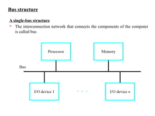
Bus structure
A single-busstructure
The interconnection network that connects the components of the computer
is called bus
35.
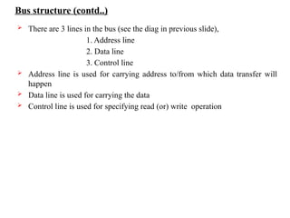
Bus structure (contd..)
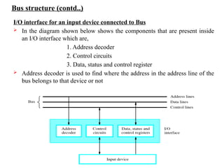
I/Ointerface for an input device connected to Bus
In the diagram shown below shows the components that are present inside
an I/O interface which are,
1. Address decoder
2. Control circuits
3. Data, status and control register
Address decoder is used to find where the address in the address line of the
bus belongs to that device or not
36.
Bus structure (contd..)
There are 3 lines in the bus (see the diag in previous slide),
1. Address line
2. Data line
3. Control line
Address line is used for carrying address to/from which data transfer will
happen
Data line is used for carrying the data
Control line is used for specifying read (or) write operation
37.
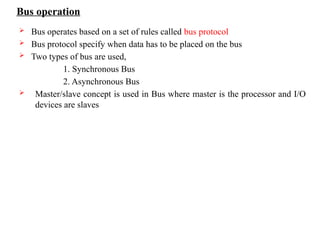
Bus operation
Busoperates based on a set of rules called bus protocol
Bus protocol specify when data has to be placed on the bus
Two types of bus are used,
1. Synchronous Bus
2. Asynchronous Bus
Master/slave concept is used in Bus where master is the processor and I/O
devices are slaves
38.
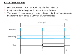
1. Synchronous Bus
On a synchronous bus, all bus sends data based on bus clock
Every read/write is completed in one clock cycle duration
The below diagram shows the timing diagram for Read operation(data
transfer from input device to CPU) on a synchronous bus
39.
1. Synchronous Bus(contd..)
Read Operation
In the diagram shown in pervious slide for read, the following things happen
1. At time t0, the master places the device address on the address lines and
sends a command on the control lines indicating a Read operation.
2. All devices to decode the address and control signals, so that the addressed
device (the slave) can respond at time t1 by placing the requested input
data on the data lines.
3. At the end of the clock cycle, at time t2, the master loads the data on the
data lines into one of its registers.
40.
1. Synchronous Bus(contd..)
Write Operation
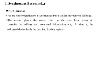
For the write operation on a synchronous bus a similar procedure is followed.
The master places the output data on the data lines when it
transmits the address and command information at t0. At time t2, the
addressed device loads the data into its data register
41.
1. Synchronous Bus(contd..)
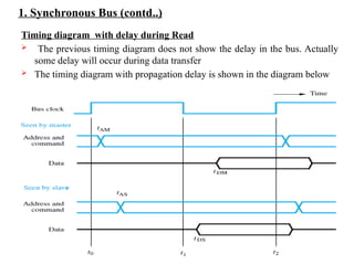
Timing diagram with delay during Read
The previous timing diagram does not show the delay in the bus. Actually
some delay will occur during data transfer
The timing diagram with propagation delay is shown in the diagram below
42.
1. Synchronous Bus(contd..)
Timing diagram with delay during Read
In the diagram shown in pervious slide for read, the following things happen
1. The master sends the address and command signals at the beginning of the
clock cycle (at t0).
2.These signals do not actually appear on the bus until tAM, largely due to the
delay in the electronic circuit from the master to the bus lines.
3. At tAS, the signals reach the slave. The slave decodes the address, and at t1
sends the requested data. Here again, the data signals do not appear on the bus
until tDS. They travel toward the master and arrive at tDM.
4. At t2, the master loads the data into its register. The data must continue to be
valid after t2 for a period equal to the hold time requirement of the register
43.
1. Synchronous Bus(contd..)
Disadvantages in single clock cycle data transfer
The disadvantage in single clock cycle data transfer is that all devices must
transfer data within one clock cycle.
This one clock cycle duration is based on speed of the slowest device. This
forces all devices to operate at the speed of slowest device
And also master has no way of determining where the slave has responded or
not. If slave does not operate correctly the error will not be detected
Multiple cycle Data Transfer
To overcome the disadvantages of single clock cycle, multiple clock cycle data
transfer comes into picture
In this scheme each device can transfer data at its own speed
They make it possible to adjust the duration of the data transfer period to match
the response speeds of different devices. This is accomplished by allowing a
complete data transfer operation to span several clock cycles. Then, the
number of clock cycles involved can vary from one device to another.
Most buses incorporate control signals that represent a response from the
device. These signals inform the master that the slave has recognized its
address and that it is ready to participate in a data transfer operation (Slave
Ready signal).
44.
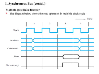
1. Synchronous Bus(contd..)
Multiple cycle Data Transfer
The diagram below shows the read operation in multiple clock cycle
45.
1. Synchronous Bus(contd..)
Multiple cycle Data Transfer
The diagram in previous slide is explained below,
During clock cycle 1, the master sends address and command information
on the bus, requesting a Read operation.
The slave receives this information and decodes it. It begins to access the
requested data at the beginning of clock cycle 2.
Due to the delay involved in getting the data, the slave cannot respond
immediately. The data become ready and are placed on the bus during clock
cycle 3. The slave asserts a control signal called Slave-ready at the same
time
The master, which has been waiting for this signal, loads the data into its
register at the end of the clock cycle.
The slave removes its data signals from the bus and returns its Slave-ready
signal to the low level at the end of cycle 3.
46.
2. Asynchronous Bus
On an asynchronous bus, no clock signal is used
Asynchronous bus does the data transfer based on Handshake protocol
between master and slave
In this handshake protocol, a control line called Master-ready is send by
master to indicate that it is ready to start a data transfer. The slave responds
by sending Slave-ready signal
The Master-ready signal is an indication to all slaves that the master has
placed the address and control information on the bus. Slave-ready signal is
an indication to master that the slave has responded to master request
47.
2. Asynchronous Bus(contd..)
Handshake control for data transfer during an input(read) operation
48.
2. Asynchronous Bus(contd..)
Handshake control for data transfer during an input(read) operation
The diagram shown in the previous slide is explained as below,
t0 - The master places the address and command information on the bus
t1 - The master sets the Master-ready line to 1 to inform the devices that it has
placed address and command information on the bus. The time gap t1 −
t0 is intended to allow for any skew(delay) that may occur on the bus.[Skew
occurs when two signals transmitted simultaneously from one source may
arrive at destination at different times (ie) In order to ensure Master- ready
signal should not reach slave before address and command information after
some time gap Master-ready signal is sent]
t2 – The Master-ready signal reach the slave. The selected slave, having decoded
the address and command information, place its data on the data lines. At
the same time, it sets the Slave-ready signal to 1
49.
2. Asynchronous Bus(contd..)
Handshake control for data transfer during an input(read) operation
t3 - The Slave-ready signal arrives at the master, indicating that the input data are
available on the bus. The master loads the data into its register. Then it drops
the Master- ready signal, indicating that it has received the data.
t4 - The master removes the address and command information from the bus.
The time gap between t3 and t4 is again intended to allow for bus skew.
[Master-ready signal should stopped first after that only address and command
information should be removed]
t5 – The slave knows master has stopped Master-ready signal, so it removes the
data and the Slave-ready signal from the bus. This completes the input
transfer.
50.
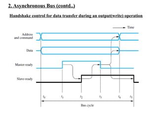
2. Asynchronous Bus(contd..)
Handshake control for data transfer during an output(write) operation
51.
2. Asynchronous Bus(contd..)
Handshake control for data transfer during an output(write) operation
The diagram shown in the previous slide is explained as below,
t0 - The master places the address and command information , data on the bus
t1 - The master sets the Master-ready line to 1 to inform the devices that it has
placed address and command information and data on the bus.
t2 – The Master-ready signal reach the slave. The selected slave loads the data
send by master into its register. At the same time, it sets the Slave-ready
signal to 1
t3 - The Slave-ready signal arrives at the master. Then master drops the Master-
ready signal
t4 - The master removes the address and command information and data from
the bus.
t5 – The slave removes the Slave-ready signal from the bus. This completes the
output transfer.
52.
2. Asynchronous Bus(contd..)
Since change in one signal is based on change in the other signal(Master-
ready and Slave-ready signals), handshake signals are said to be fully
interlocked
Hence Handshake protocol is also called as Full handshake protocol
53.
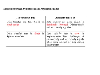
Difference between Synchronousand Asynchronous Bus
Synchronous Bus Asynchronous Bus
Data transfer are done based on
clock cycles
Data transfer are done based on
Handshake Protocol (Master-ready
and slave-ready signals)
Data transfer rate is faster in
Synchronous bus
Data transfer rate is slow in
Asynchronous bus. Exchange of
master-ready and slave-ready signals
takes some amount of time during
data transfer
54.
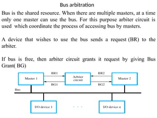
Bus arbitration
Bus isthe shared resource. When there are multiple masters, at a time
only one master can use the bus. For this purpose arbiter circuit is
used which coordinate the process of accessing bus by masters.
A device that wishes to use the bus sends a request (BR) to the
arbiter.
If bus is free, then arbiter circuit grants it request by giving Bus
Grant( BG)
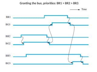
The master 1has the highest priority, followed by the others
in increasing numerical order.
Master 2 sends a request to use the bus first. Since there are
no other requests, the arbiter grants the bus to this master by
asserting BG2. When master 2 completes its data transfer
operation, it releases the bus by deactivating BR2.
By that time, both masters 1 and 3 have activated their
request lines. Since device 1 has a higher priority, the arbiter
activates BG1 after it deactivates BG2, thus granting the bus
to master 1.
When master 1 releases the bus by deactivating BR1, the
arbiter deactivates BG1 and activates BG3 to grant the bus to
master 3. The bus is granted to master 1 before master 3 even
though master 3 activated its request line before master 1.
57.
Interconnection Standards
A typicaldesktop or notebook computer has several ports that can be used to connect
I/O devices, such as a mouse, a memory key, or a disk drive. IEEE (Institute of
Electrical and Electronics Engineers) develops standards for I/O interfaces.
Universal Serial Bus (USB)
USB is the most widely used interconnection standard. A large variety of devices are
available with a USB connector, including mouse, disk drives, printers, cameras, and
many more. The commercial success of the USB is due to its simplicity and low cost.
The original USB specification supports two speeds of operation, called low-speed (1.5
Megabits/s) and full-speed (12 Megabits/s). Later, USB 2 called High-Speed USB
enables data transfers at speeds up to 480 Megabits/s. As I/O devices continued to
evolve with even higher speed requirements, USB3 (called Super speed) was
developed to support data transfer rates up to 5 Gigabits/s.
58.
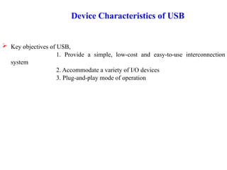
Device Characteristics ofUSB
Key objectives of USB,
1. Provide a simple, low-cost and easy-to-use interconnection
system
2. Accommodate a variety of I/O devices
3. Plug-and-play mode of operation
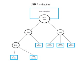
The USB usespoint-to-point connections and a serial
transmission format. When multiple devices are connected,
they are arranged in a tree structure. Each node of the tree has
a device called a hub, which acts as an intermediate transfer
point between the host computer and the I/O devices.
At the root of the tree, a root hub connects the entire tree to
the host computer. The leaves of the tree are the I/O devices: a
mouse, a keyboard, a printer, an Internet connection, a camera,
or a speaker. The tree structure makes it possible to connect
many devices using simple point-to-point serial links.
If I/O devices are allowed to send messages at any time, two
messages may reach the hub at the same time and interfere
with each other. For this reason, the USB operates strictly
on the basis of polling.
61.
A device maysend a message only in response to a poll
message from the host processor. Hence, no two devices can
send messages at the same time. This restriction allows hubs to
be simple, low-cost devices.
When a device is first connected to a hub, or when it is
powered on, it has the address 0. Periodically, the host polls
each hub to collect status information and learn about new
devices that may have been added or disconnected.
When the host is informed that a new device has been
connected, it reads the information in a special memory in the
device’s USB interface to know about the device’s
capabilities.
It then assigns the device a unique USB address and writes
that address in one of the device’s interface registers. It is this
initial connection procedure that gives the USB its plug-and-
play capability.
62.
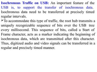
Isochronous Traffic onUSB: An important feature of the
USB is, to support the transfer of isochronous data.
Isochronous data need to be transferred at precisely timed
regular intervals.
To accommodate this type of traffic, the root hub transmits a
uniquely recognizable sequence of bits over the USB tree
every millisecond. This sequence of bits, called a Start of
Frame character, acts as a marker indicating the beginning of
isochronous data, which are transmitted after this character.
Thus, digitized audio and video signals can be transferred in a
regular and precisely timed manner.


![2. Asynchronous Bus (contd..)
Handshake control for data transfer during an input(read) operation
The diagram shown in the previous slide is explained as below,
t0 - The master places the address and command information on the bus
t1 - The master sets the Master-ready line to 1 to inform the devices that it has
placed address and command information on the bus. The time gap t1 −
t0 is intended to allow for any skew(delay) that may occur on the bus.[Skew
occurs when two signals transmitted simultaneously from one source may
arrive at destination at different times (ie) In order to ensure Master- ready
signal should not reach slave before address and command information after
some time gap Master-ready signal is sent]
t2 – The Master-ready signal reach the slave. The selected slave, having decoded
the address and command information, place its data on the data lines. At
the same time, it sets the Slave-ready signal to 1](https://image.slidesharecdn.com/unit5ioorganization-260120173756-ad55042e/85/Input-and-output-organization-under-computer-organization-48-320.jpg)
![2. Asynchronous Bus (contd..)
Handshake control for data transfer during an input(read) operation
t3 - The Slave-ready signal arrives at the master, indicating that the input data are
available on the bus. The master loads the data into its register. Then it drops
the Master- ready signal, indicating that it has received the data.
t4 - The master removes the address and command information from the bus.
The time gap between t3 and t4 is again intended to allow for bus skew.
[Master-ready signal should stopped first after that only address and command
information should be removed]
t5 – The slave knows master has stopped Master-ready signal, so it removes the
data and the Slave-ready signal from the bus. This completes the input
transfer.](https://image.slidesharecdn.com/unit5ioorganization-260120173756-ad55042e/85/Input-and-output-organization-under-computer-organization-49-320.jpg)