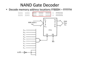
- Memory interfacing in microprocessor systems involves two main types of memory: read-only memory (ROM) and random access memory (RAM).
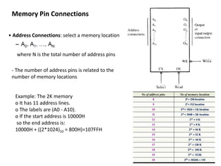
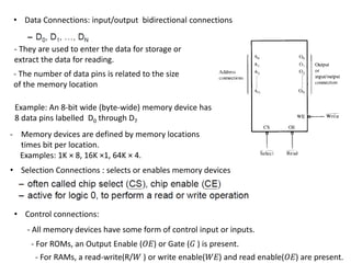
- Memory is made up of semiconductor devices with each bit stored in a memory cell consisting of transistors. The capacity of a memory chip depends on the number of address pins determining the number of memory locations and data pins determining the number of bits stored per location.
- The two major types of memory are RAM, which can be read from and written to, and ROM, which can only be read from. Common ROM types include PROM, EPROM, and EEPROM, while common RAM types are SRAM and DRAM.


![INTERFACING2 [Autosaved] interfacing in Computer system](https://cdn.slidesharecdn.com/ss_thumbnails/interfacing2autosaved-250404124048-193f189f-thumbnail.jpg?width=640&height=640&fit=bounds)