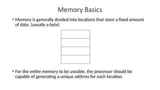
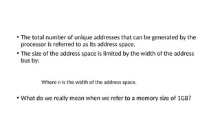
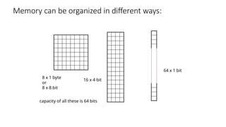
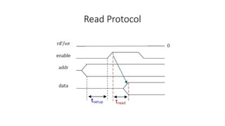
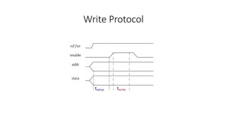
Memory Interfacing
Memory Basics
• Memory is generally divided into locations that store a fixed amount
of data. (usually a byte)
• For the entire memory to be useable, the processor should be
capable of generating a unique address for each location.
• The total number of unique addresses that can be generated by the
processor is referred to as its address space.
• The size of the address space is limited by the width of the address
bus by:
Where n is the width of the address space.
• What do we really mean when we refer to a memory size of 1GB?
Memory connections
Address Connections
• All memory devices have address inputs that select a memory
location within the memory device.
• They are usually labelled from the least significant address input to ,
the most significant.
• A 1K device has 10 address pins; labelled .
• Memory addresses are usually represented in hexadecimal.
• Example: 400H represents 1K-bytes. If a memory device is decoded to
begin at address 1000H, and it is a 1K device, what is the address of
the last memory location?
• Others you should keep in mind: 1000H : 4K, 10000H : 64K, etc
Practical Application
Processors have a limit on how
much memory they can make
use of based on the address
space.
Memory can be organized in different ways:
8 x 1 byte
or
8 x 8 bit
16 x 4 bit
64 x 1 bit
capacity of all these is 64 bits
Data Connections
• All memory devices have a set of data outputs or input/outputs. The
figure in slide 4 has a set of common I/O pins.
• The data connections are the points at which data is entered for
writing or extracted for reading.
• Data pins on memory devices are almost always labelled Do – D7 for an
8-bit wide memory device. (Often called byte-wide memory)
• It is however possible to have 16-bits, 4-bits, or just 1-bit wide
memory devices.
• Catalogue listings of memory devices often refer to memory locations
times bits per location.
• Example: 1K x 8, 16k x 1, etc.
• Memory devices are also classified according to the total bit capacity.
• Example: 1K x 8 may be listed as 8K, 64K x 4 as 256K, etc
• Variations occur across manufacturers.
TEST YOUR UNDERSTANDING!
• Why is the data bus bi-directional?
• If a 32 bit microprocessor system is designed to access a memory
system of total of 256 K bytes what is the data bus and the address
bus lengths of the system.
Selection Connections
• Each memory device has an input that selects or enables the device.
• (Refer again to image on Slide 4)
• This input is often called a chip select (CS or ) or chip enable (CE or ).
It is sometimes simply referred to as a Select (S or ) input.
• If this input is active the memory device performs a read or write. If it
is inactive, the memory device is disabled.
Control Connections
• All memory devices have some form of control input(s).
• This input determines what kind of action is performed on the device.
• A ROM usually has one control input, the output connection ( or gate
( input. (Why?)
• A RAM device has one or two control inputs.
• If there exists only one control input it is usually labelled .
• If there are two control inputs, they are labelled and
Read and Write Protocols
Timing Diagrams
• Most common method for describing a communication protocol is by
the use of timing diagrams.
• On a timing diagram, time proceeds to the right on x-axis.
• A control signal is shown with a single line and may by low or high at
some intervals.
• A signal may be active low (e.g., G’, , or G_L).
• The term assert is used to indicate that the signal is made active and
deassert means deactivated. Asserting G means set G=0.
• Deassert for an active low signal:
• Data signals on the other hand are usually represented by a single line
when inactive and a ‘double’ line when active.
Read Protocol
Write Protocol
TEST YOUR UNDERSTANDING…
•Can you explain the difference between these
three terms:
•Setup time, read time, write time?
Assignment.
 Read about different types of memory systems in use in today’s
industry.
 ROM, RAM, Disk, Cache, etc.

Microprocessor memory interfacing basics

  • 1.
  • 2.
    Memory Basics • Memoryis generally divided into locations that store a fixed amount of data. (usually a byte) • For the entire memory to be useable, the processor should be capable of generating a unique address for each location.
  • 3.
    • The totalnumber of unique addresses that can be generated by the processor is referred to as its address space. • The size of the address space is limited by the width of the address bus by: Where n is the width of the address space. • What do we really mean when we refer to a memory size of 1GB?
  • 4.
  • 5.
    Address Connections • Allmemory devices have address inputs that select a memory location within the memory device. • They are usually labelled from the least significant address input to , the most significant. • A 1K device has 10 address pins; labelled . • Memory addresses are usually represented in hexadecimal. • Example: 400H represents 1K-bytes. If a memory device is decoded to begin at address 1000H, and it is a 1K device, what is the address of the last memory location? • Others you should keep in mind: 1000H : 4K, 10000H : 64K, etc
  • 6.
    Practical Application Processors havea limit on how much memory they can make use of based on the address space.
  • 7.
    Memory can beorganized in different ways: 8 x 1 byte or 8 x 8 bit 16 x 4 bit 64 x 1 bit capacity of all these is 64 bits
  • 8.
    Data Connections • Allmemory devices have a set of data outputs or input/outputs. The figure in slide 4 has a set of common I/O pins. • The data connections are the points at which data is entered for writing or extracted for reading. • Data pins on memory devices are almost always labelled Do – D7 for an 8-bit wide memory device. (Often called byte-wide memory) • It is however possible to have 16-bits, 4-bits, or just 1-bit wide memory devices.
  • 9.
    • Catalogue listingsof memory devices often refer to memory locations times bits per location. • Example: 1K x 8, 16k x 1, etc. • Memory devices are also classified according to the total bit capacity. • Example: 1K x 8 may be listed as 8K, 64K x 4 as 256K, etc • Variations occur across manufacturers.
  • 10.
    TEST YOUR UNDERSTANDING! •Why is the data bus bi-directional? • If a 32 bit microprocessor system is designed to access a memory system of total of 256 K bytes what is the data bus and the address bus lengths of the system.
  • 11.
    Selection Connections • Eachmemory device has an input that selects or enables the device. • (Refer again to image on Slide 4) • This input is often called a chip select (CS or ) or chip enable (CE or ). It is sometimes simply referred to as a Select (S or ) input. • If this input is active the memory device performs a read or write. If it is inactive, the memory device is disabled.
  • 12.
    Control Connections • Allmemory devices have some form of control input(s). • This input determines what kind of action is performed on the device. • A ROM usually has one control input, the output connection ( or gate ( input. (Why?) • A RAM device has one or two control inputs. • If there exists only one control input it is usually labelled . • If there are two control inputs, they are labelled and
  • 13.
    Read and WriteProtocols Timing Diagrams • Most common method for describing a communication protocol is by the use of timing diagrams. • On a timing diagram, time proceeds to the right on x-axis. • A control signal is shown with a single line and may by low or high at some intervals. • A signal may be active low (e.g., G’, , or G_L). • The term assert is used to indicate that the signal is made active and deassert means deactivated. Asserting G means set G=0.
  • 14.
    • Deassert foran active low signal: • Data signals on the other hand are usually represented by a single line when inactive and a ‘double’ line when active.
  • 15.
  • 16.
  • 17.
    TEST YOUR UNDERSTANDING… •Canyou explain the difference between these three terms: •Setup time, read time, write time?
  • 18.
    Assignment.  Read aboutdifferent types of memory systems in use in today’s industry.  ROM, RAM, Disk, Cache, etc.

Editor's Notes

  • #1 See chapter Nine of Text book.