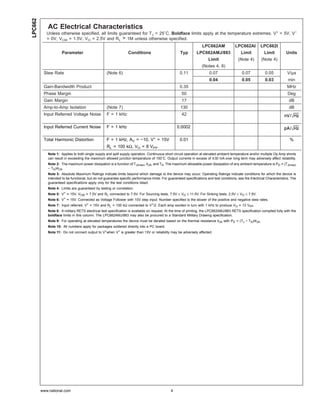
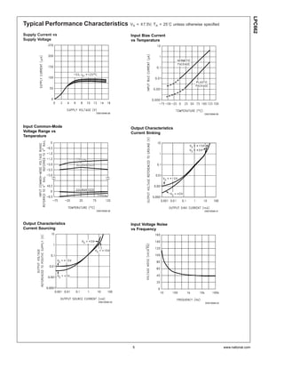
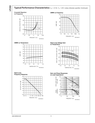
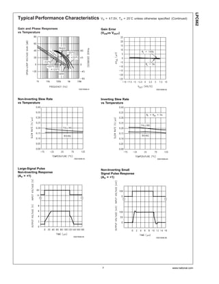
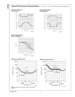
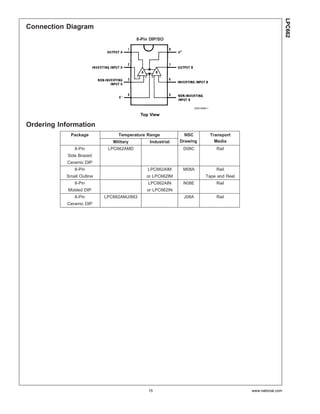
This document provides information on the LPC662 low power CMOS dual operational amplifier:
- It is ideal for single supply operation from +5V to +15V with rail-to-rail output swing and input common-mode range including ground.
- Key features include micropower operation (<0.5mW), high voltage gain (120dB), low input offset voltage (3mV), and ultra low input bias current (2fA).
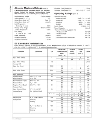
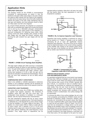
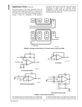
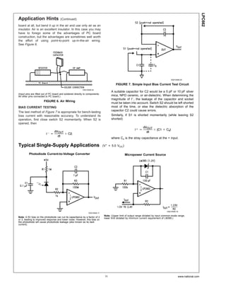
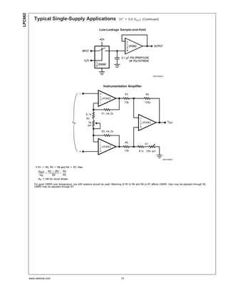
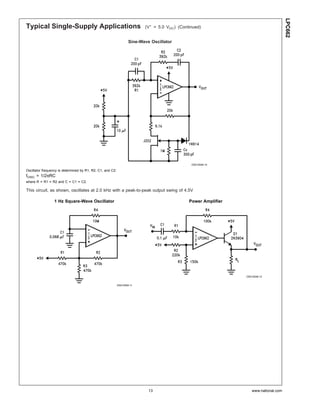
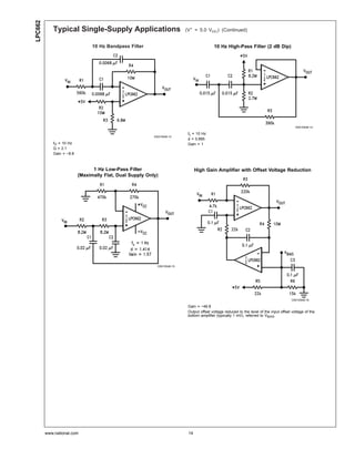
- Applications include high-impedance buffer, precision current-to-voltage converter, long-term integrator, high-impedance preamplifier, active filter, sample-and-hold circuit, and peak detector.