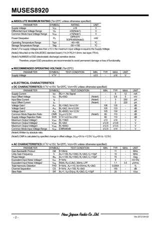
The MUSES8920 is a high quality audio J-FET input dual operational amplifier. It has low noise of 8nV/√Hz, high slew rate of 25V/μs, and low distortion of 0.00004% at a voltage gain of 1. These characteristics make it suitable for applications such as audio preamplifiers, active filters, and line amplifiers. It can also be used in transimpedance amplifiers due to its low input bias current. The MUSES8920 is available in an 8-pin DIP or SOP package. It operates from a ±3.5V to ±16V power supply and provides high performance audio amplification.

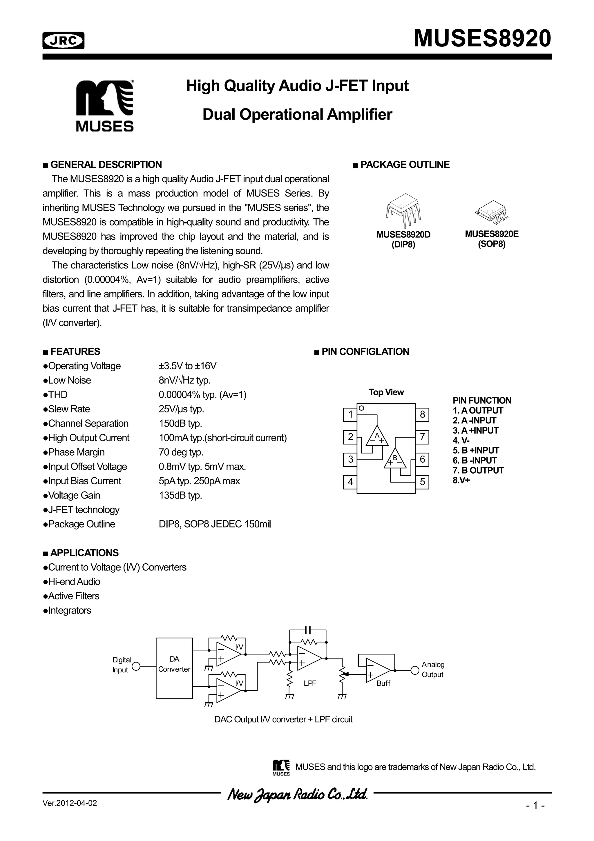
![MUSES8920
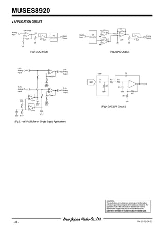
■ Application Notes
●Package Power, Power Dissipation and Output Power
IC is heated by own operation and possibly gets damage when the junction power exceeds the acceptable value called
Power Dissipation PD. The dependence of the MUSES8920 PD on ambient temperature is shown in Fig 1. The plots are
depended on following two points. The first is PD on ambient temperature 25ºC, which is the maximum power dissipation.
The second is 0W, which means that the IC cannot radiate any more. Conforming the maximum junction temperature
Tjmax to the storage temperature Tstg derives this point. Fig.1 is drawn by connecting those points and conforming the PD
lower than 25ºC to it on 25ºC. The PD is shown following formula as a function of the ambient temperature between those
points.
Tjmax - Ta
Dissipation Power PD = [W] (Ta=25ºC to Ta=150ºC)
θja
Where, ja is heat thermal resistance which depends on parameters such as package material, frame material and so on.
Therefore, PD is different in each package.
While, the actual measurement of dissipation power on MUSES8920 is obtained using following equation.
(Actual Dissipation Power) = (Supply Voltage VDD) X (Supply Current IDD) – (Output Power Po)
The MUSES8920 should be operated in lower than PD of the actual dissipation power.
To sustain the steady state operation, take account of the Dissipation Power and thermal design.
PD [mW]
SOP8
900
870
DIP8
Ta [deg]
-40 25 85 150
(Topr max.) (Tstg max.)
Fig.1 Power Dissipations vs. Ambient Temperature on the MUSE8920
Ver.2012-04-02 -3-](https://image.slidesharecdn.com/muses8920e-130226003755-phpapp02/85/MUSES8920-3-320.jpg)
![MUSES8920
TYPICAL CARACTERISTICS
THD+N vs. Output Voltage (Frequency) THD+N vs. Output Voltage (Frequency)
V+/V-=±15V, AV=+10, RL=2k, Ta=25ºC V+/V-=±3.5V, AV=+10, RL=2k, Ta=25ºC
10 10
1 1
f=20Hz
THD+N [%]
THD+N [%]
0.1 0.1 f=1kHz
f=20kHz
0.01 0.01
f=1kHz
f=20kHz
f=20kHz
0.001 0.001
0.0001 0.0001
0.01 0.1 1 10 100 0.01 0.1 1 10 100
Output Voltage [Vrms] Output Voltage [Vrms]
Voltage Noise vs. Frequency Channel Separation vs. Frequency
+ - + -
∞
V /V =±15V, AV=+100, RS=100Ω, RL=∞, Ta=25ºC V /V =±15V, AV=-100, RL=2kΩ, Ta=25ºC
100 -120
-125
Equivalent Input Noise Voltage
80
Channel Separation [dB]
-130
60 -135
[nV/√ Hz]
-140
40 -145
-150
20
-155
0 -160
1 10 100 1k 10k 100k 10 100 1k 10k 100k
Frequency [Hz] Frequency [Hz]
Gain vs. Frequency (Temperature) Phase Margin vs. Temperature (Supply Voltage)
+ - + -
V /V =±15V, AV=+100, RL=2kΩ, CL=10pF V /V =±15V, AV=+100, RS=100Ω, RL=2kΩ, CL=10pF, VIN=-30dBm
60 90
Gain
Ta=+85ºC
40
Ta=+25ºC
Phase Margin [deg]
V+/V-=±15V
Voltage Gain [dB]
Phase Ta=-40ºC
20 0 80
Phase [deg]
0 -45
-20 Ta=+85ºC -90 70
Ta=+25ºC Ta=-40ºC
V+/V-=±3.5V
-40 -135
-60 -180 60
10k 100k 1M 10M 100M -50 -25 0 25 50 75 100 125 150
Frequency [Hz] Ambient Temperature [ºC]
-4- Ver.2012-04-02](https://image.slidesharecdn.com/muses8920e-130226003755-phpapp02/85/MUSES8920-4-320.jpg)
![MUSES8920
■ TYPICAL CARACTERISTICS
Pulse Response Slew Rate vs. Temperature
+ - + -
V /V =±15V, Gv=0dB, CL=10pF, RL=2kΩ, Ta=25ºC V /V =±15V, VIN=2VP-P, f=100kHz, Gv=0dB, CL=10pF, RL=2kΩ
80
Input
70
60
Fall
Slew Rate [V/µs]
Voltage [1V/div]
50
40
30
20
Rise
10
Output
0
Time [1µs/div]
-50 -25 0 25 50 75 100 125 150
Ambient Temperature [ºC]
Supply Current vs. Supply Voltage (Temperature) Supply Current vs. Temperature (Supply Voltage)
AV=0dB AV=0dB
12 12
+ -
V /V =±15V
Ta=+25ºC
10 10
Supply Current [mA]
Supply Current [mA]
8 8
Ta=+85ºC Ta=-40ºC V+/V-=±3.5V
6 6
4 4
2 2
0 0
±0 ±4 ±8 ±12 ±16 -50 -25 0 25 50 75 100 125 150
+ -
Supply Voltage V /V [V] Ambient Temperature [ºC]
Input Offset Voltage vs. Supply Voltage (Temperature) Input Offset Voltage vs. Temperature (Supply Voltage)
VICM=0V, VIN=0V VICM=0V, VIN=0V
2.0 2.0
1.5 1.5
Input Offset Voltage [mV]
Input Offset Voltage [mV]
1.0 1.0 V+/V-=±15V
Ta=-40ºC
0.5 0.5
0.0 0.0
Ta=+25ºC
=
Ta=+85ºC
+ -
V /V =±3.5V
-0.5 -0.5
-1.0 -1.0
0 ±4 ±8 ±12 ±16 -50 -25 0 25 50 75 100 125 150
+ -
Supply Voltage V /V [V] Ambient Temperature [ºC]
Ver.2012-04-02 -5-](https://image.slidesharecdn.com/muses8920e-130226003755-phpapp02/85/MUSES8920-5-320.jpg)
![MUSES8920
■ TYPICAL CARACTERISTICS
Input Offset Voltage Input Offset Voltage
vs. Common Mode Input Voltage vs. Common Mode Input Voltage
(Temperature) (Temperature)
V+/V-=±15V V+/V-=±3.5V
2.0 2.0
1.5 1.5
Input Offset Voltage [mV]
Input Offset Voltage [mV]
1.0 Ta=-40ºC 1.0
Ta=-40ºC
0.5 0.5
0.0 0.0
Ta=+25ºC
= Ta=+85ºC
Ta=+25ºC
=
Ta=+85ºC
-0.5 -0.5
-1.0 -1.0
-15 -10 -5 0 5 10 15 -4 -3 -2 -1 0 1 2 3 4
Common Mode Input Voltage [V] Common Mode Input Voltage [V]
Input Bias Current vs. Common Mode Input Voltage
Input Bias Current vs. Temperature (Supply Voltage) (Temperature)
+ - + -
VICM=0V, V /V =±15V V /V =±15V, Ta=25ºC
1000n 10
100n 9
Input Bias Current [A]
Input Bias Current [pA]
8
10n
7
1n
6
100p
5
10p 4
1p 3
-50 -25 0 25 50 75 100 125 150 -15 -10 -5 0 5 10 15
Ambient Temperature [ºC] Common Mode Input Voltage [V]
CMR vs. Temperature SVR vs. Temperature
+ - + -
V /V =±15V →
VICM=0V, V /V =±3.5V→±16V
140 140
Supply Voltage Rejection Ratio [dB]
Common Mode Rejection Ratio [dB]
130 130
→
VICM=0V→+12.5V
120 120
110 110
100 100
→
VICM=-12.5V→0V
90 90
80 80
-50 -25 0 25 50 75 100 125 150 -50 -25 0 25 50 75 100 125 150
Ambient Temperature [ºC] Ambient Temperature [ºC]
-6- Ver.2012-04-02](https://image.slidesharecdn.com/muses8920e-130226003755-phpapp02/85/MUSES8920-6-320.jpg)
![MUSES8920
■ TYPICAL CARACTERISTICS
Output Voltage vs. Output Current (Temperature) Output Voltage vs. Output Current (Temperature)
+ - + -
V /V =±15V V /V =±3.5V
15 4
Isource
Isource 3 Ta=+125ºC
10 Ta=-40ºC
Ta=+85ºC
2
Output Voltage [V]
Output Voltage [V]
Ta=+25ºC
5 Ta=+25ºC
1
Ta=-40ºC
0 0
Ta=+85ºC -1
-5
Ta=+25ºC Ta=-40ºC
-2
-10
Isink -3 Isink
-15 -4
1 10 100 1k 1 10 100 1k
Output Current [mA] Output Current [mA]
Maximum Output Voltage vs. Load Resistance Maximum Output Voltage vs. Load Resistance
(Temperature) (Temperature)
+ - + -
V /V =±15V, Gv=open, RL to 0V V /V =±3.5V, Gv=open, RL to 0V
15 4
3
10
Maximum Output Voltage [V]
Maximum Output Voltage [V]
Ta=-40ºC
Ta=+25ºC 2
5
Ta=+85ºC 1
0 0
Ta=+85ºC
Ta=+25ºC
-1 Ta=-40ºC
-5
-2
-10
-3
-15 -4
10 100 1k 10k 100k 10 100 1k 10k 100k
Load Resistance [Ω] Load Resistance [Ω]
Ver.2012-04-02 -7-](https://image.slidesharecdn.com/muses8920e-130226003755-phpapp02/85/MUSES8920-7-320.jpg)