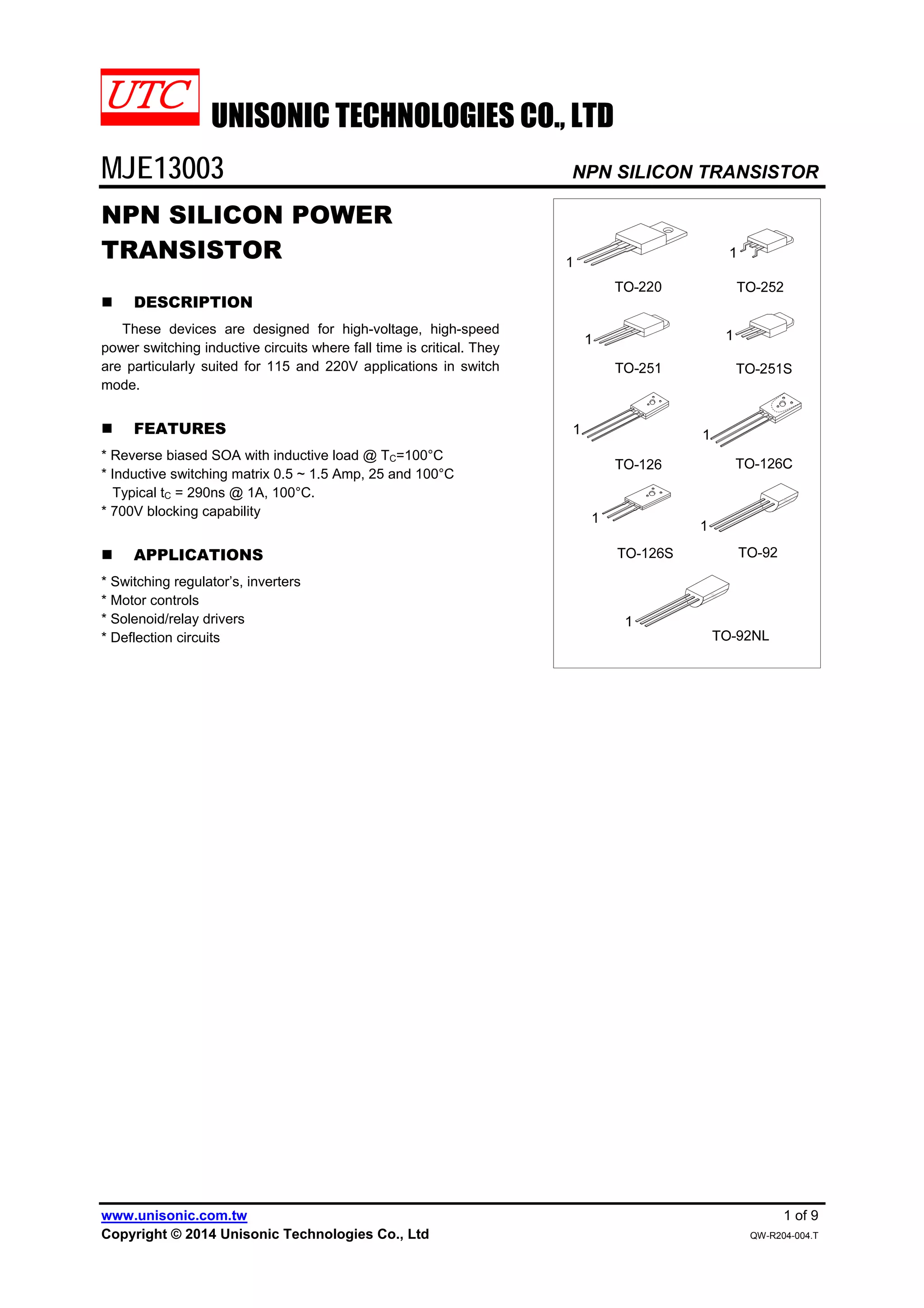
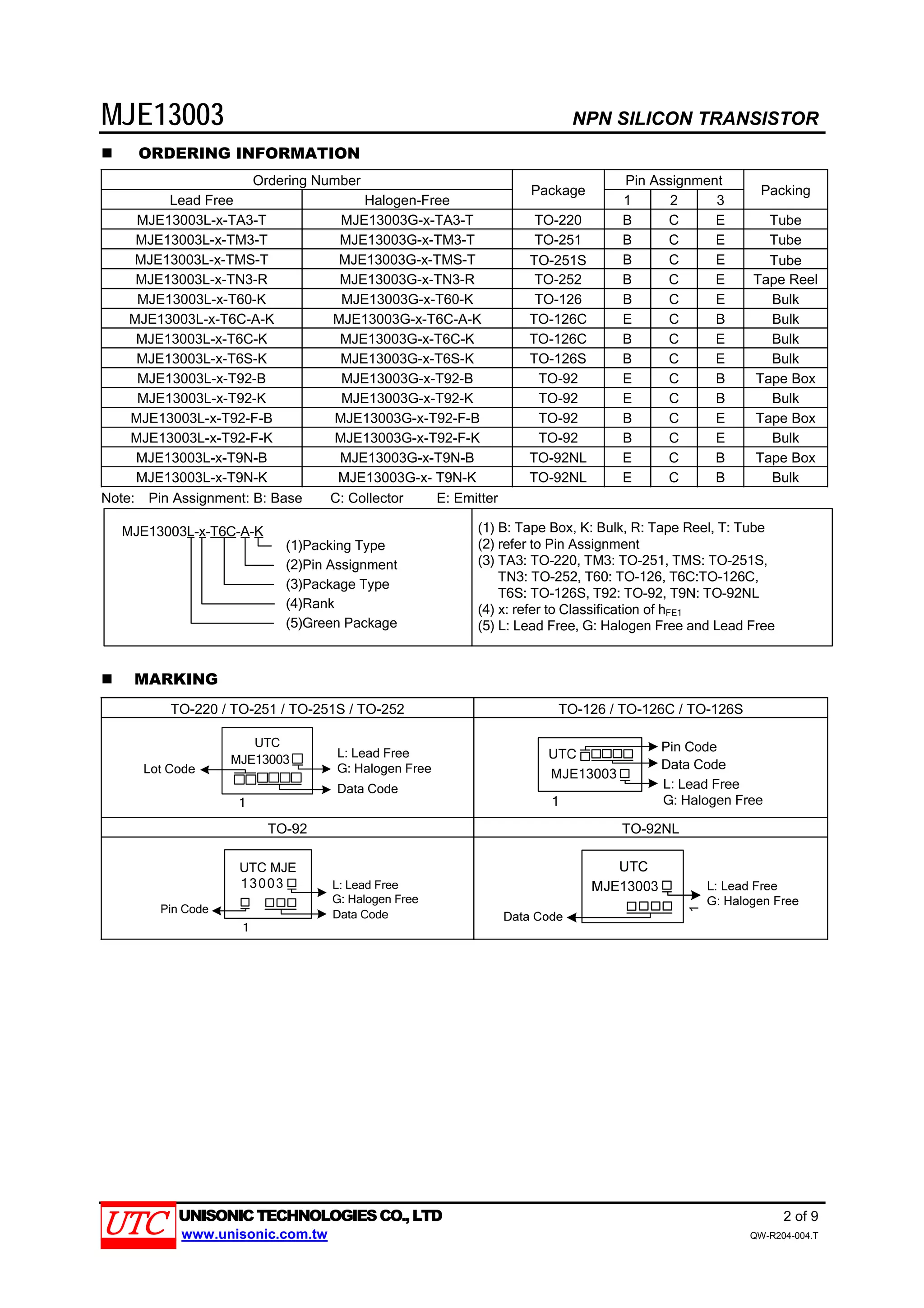
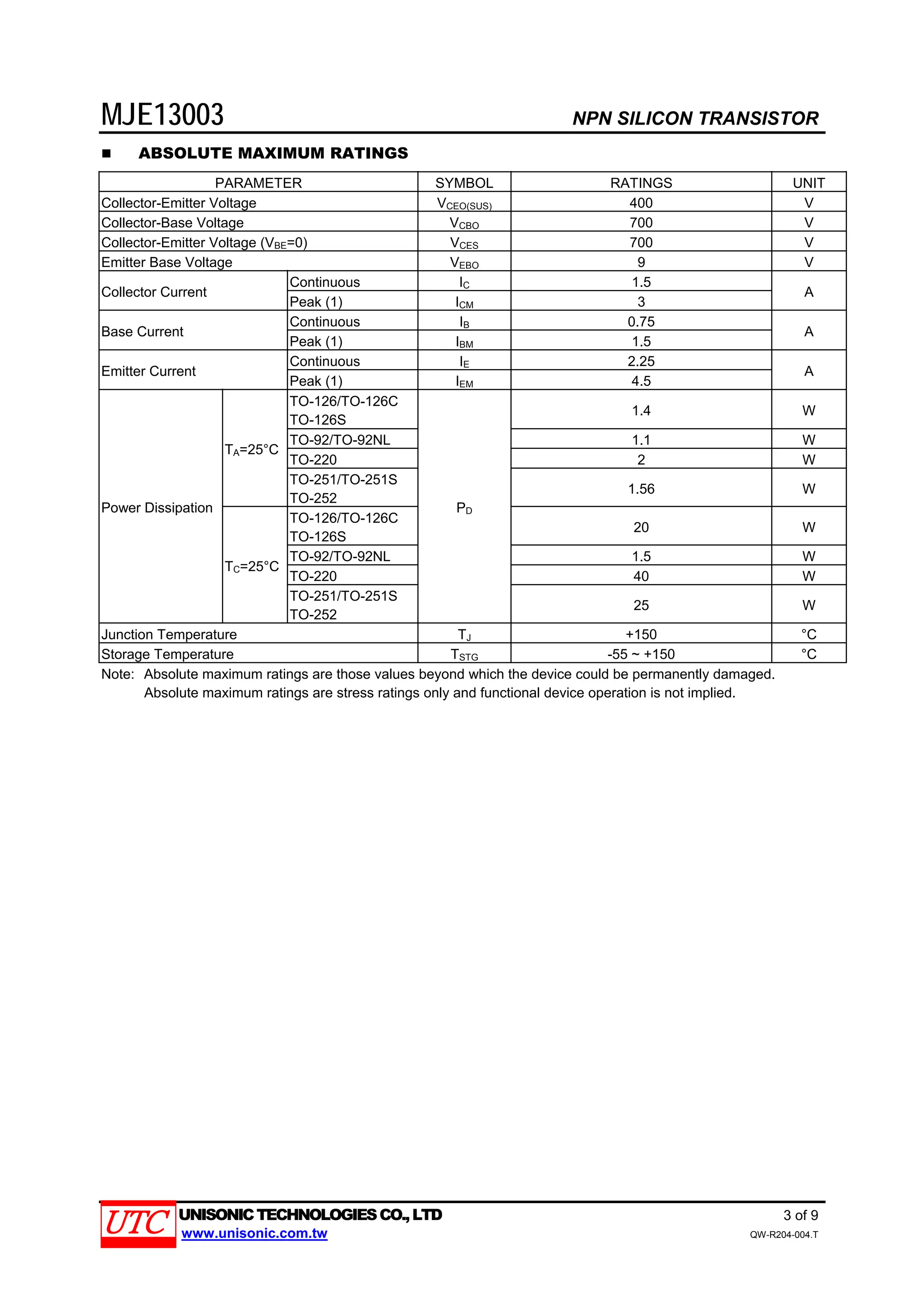
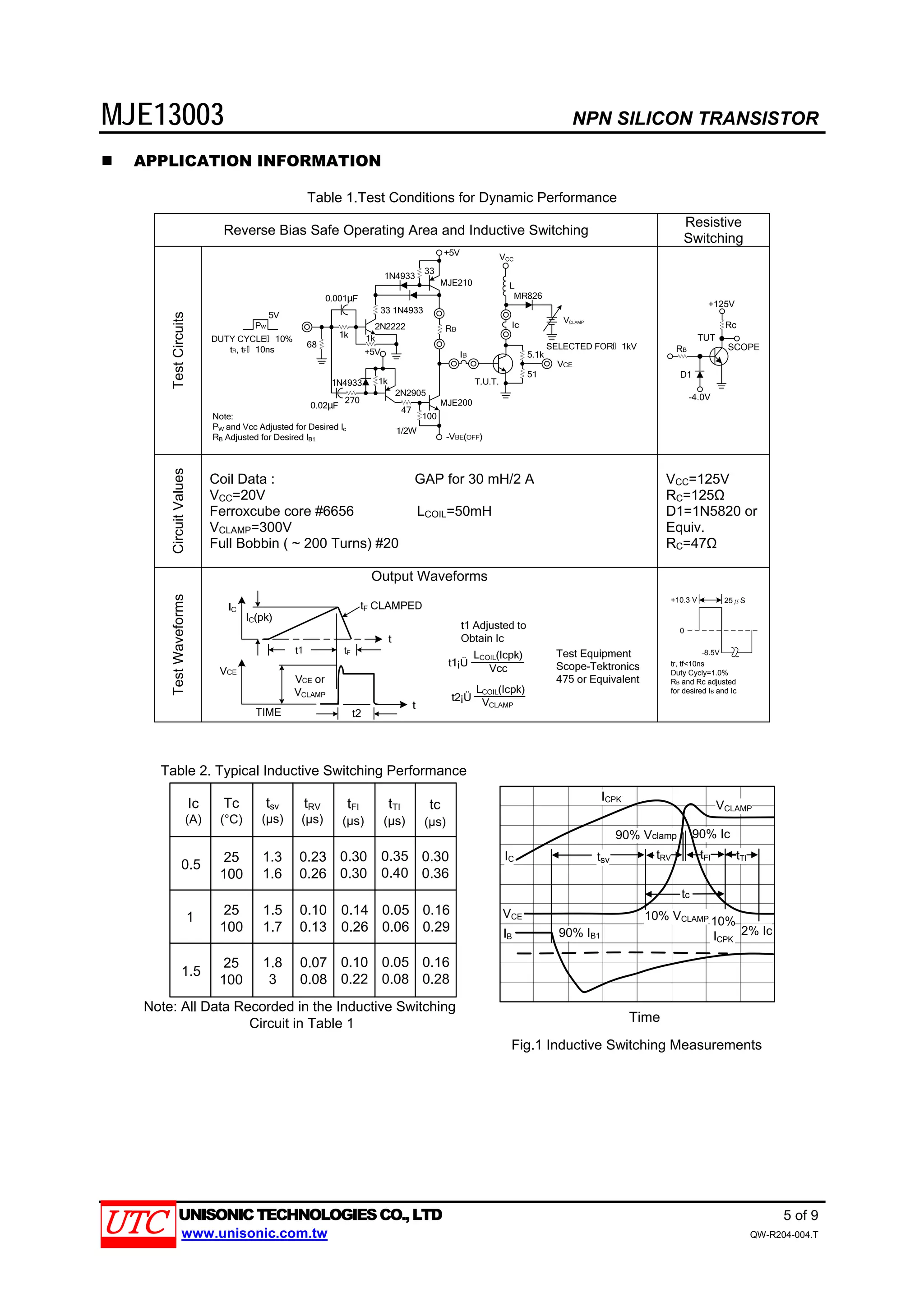
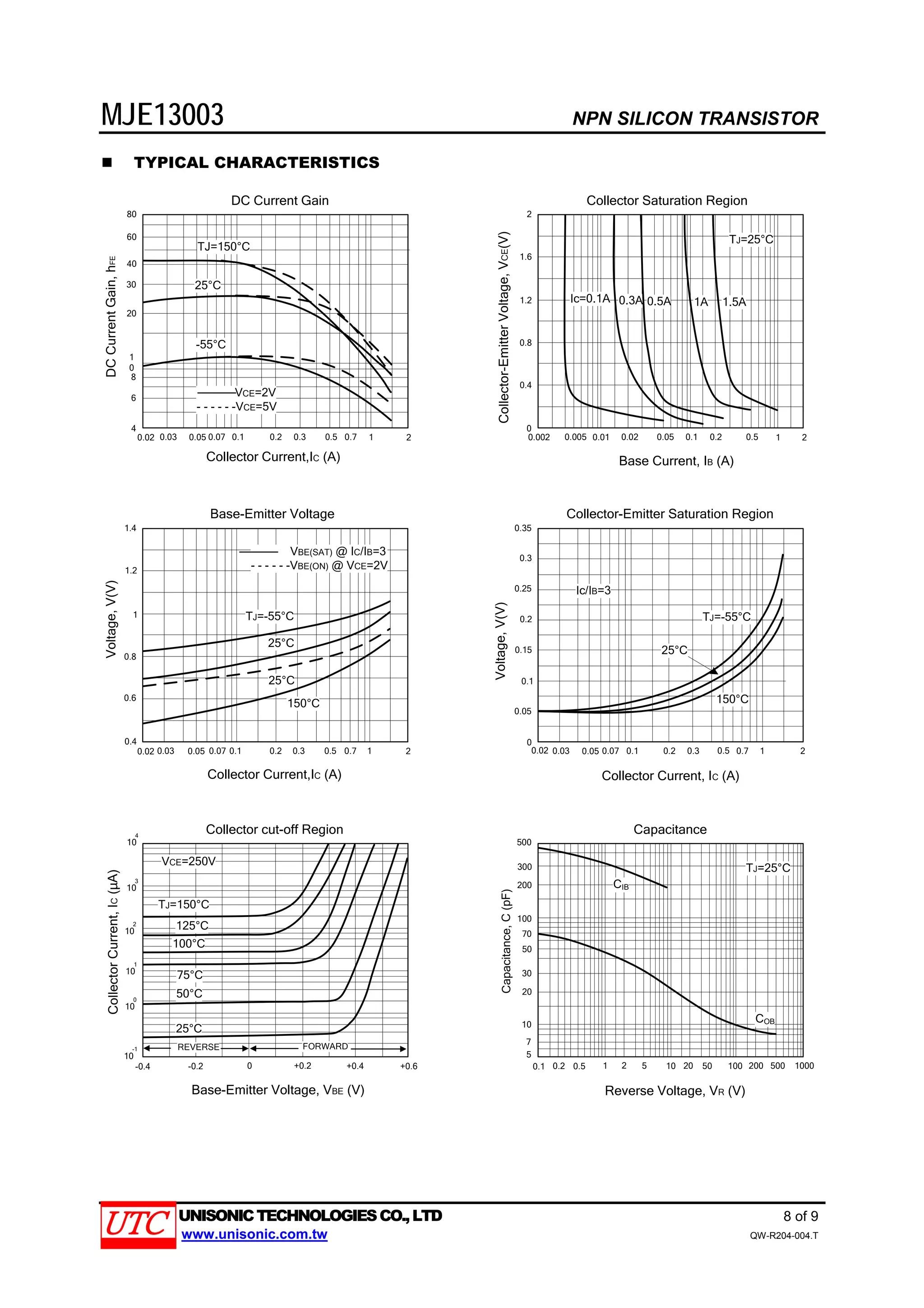
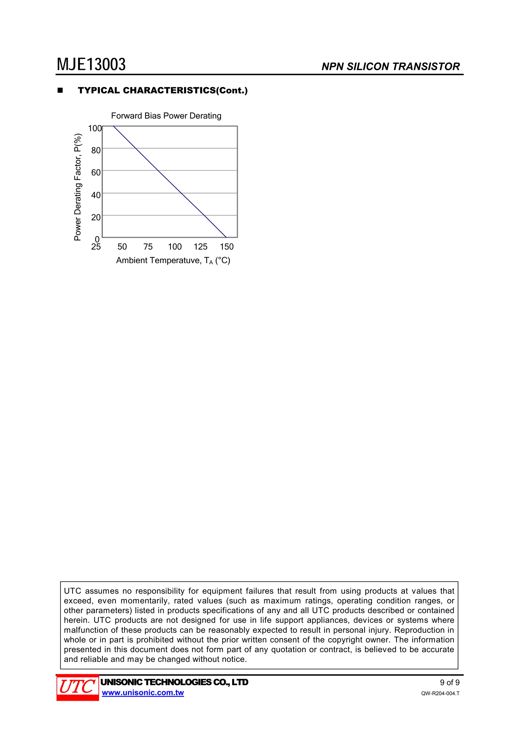
UNISONIC TECHNOLOGIES CO., LTD
MJE13003 NPN SILICON TRANSISTOR
www.unisonic.com.tw 1 of 9
Copyright © 2014 Unisonic Technologies Co., Ltd QW-R204-004.T
NPN SILICON POWER
TRANSISTOR
 DESCRIPTION
These devices are designed for high-voltage, high-speed
power switching inductive circuits where fall time is critical. They
are particularly suited for 115 and 220V applications in switch
mode.
 FEATURES
* Reverse biased SOA with inductive load @ TC=100°C
* Inductive switching matrix 0.5 ~ 1.5 Amp, 25 and 100°C
Typical tC = 290ns @ 1A, 100°C.
* 700V blocking capability
 APPLICATIONS
* Switching regulator’s, inverters
* Motor controls
* Solenoid/relay drivers
* Deflection circuits
MJE13003 NPN SILICON TRANSISTOR
UNISONICTECHNOLOGIESCO.,LTD 2 of 9
www.unisonic.com.tw QW-R204-004.T
 ORDERING INFORMATION
Ordering Number
Package
Pin Assignment
Packing
Lead Free Halogen-Free 1 2 3
MJE13003L-x-TA3-T MJE13003G-x-TA3-T TO-220 B C E Tube
MJE13003L-x-TM3-T MJE13003G-x-TM3-T TO-251 B C E Tube
MJE13003L-x-TMS-T MJE13003G-x-TMS-T TO-251S B C E Tube
MJE13003L-x-TN3-R MJE13003G-x-TN3-R TO-252 B C E Tape Reel
MJE13003L-x-T60-K MJE13003G-x-T60-K TO-126 B C E Bulk
MJE13003L-x-T6C-A-K MJE13003G-x-T6C-A-K TO-126C E C B Bulk
MJE13003L-x-T6C-K MJE13003G-x-T6C-K TO-126C B C E Bulk
MJE13003L-x-T6S-K MJE13003G-x-T6S-K TO-126S B C E Bulk
MJE13003L-x-T92-B MJE13003G-x-T92-B TO-92 E C B Tape Box
MJE13003L-x-T92-K MJE13003G-x-T92-K TO-92 E C B Bulk
MJE13003L-x-T92-F-B MJE13003G-x-T92-F-B TO-92 B C E Tape Box
MJE13003L-x-T92-F-K MJE13003G-x-T92-F-K TO-92 B C E Bulk
MJE13003L-x-T9N-B MJE13003G-x-T9N-B TO-92NL E C B Tape Box
MJE13003L-x-T9N-K MJE13003G-x- T9N-K TO-92NL E C B Bulk
Note: Pin Assignment: B: Base C: Collector E: Emitter
 MARKING
TO-220 / TO-251 / TO-251S / TO-252 TO-126 / TO-126C / TO-126S
TO-92 TO-92NL
MJE13003 NPN SILICON TRANSISTOR
UNISONICTECHNOLOGIESCO.,LTD 3 of 9
www.unisonic.com.tw QW-R204-004.T
 ABSOLUTE MAXIMUM RATINGS
PARAMETER SYMBOL RATINGS UNIT
Collector-Emitter Voltage VCEO(SUS) 400 V
Collector-Base Voltage VCBO 700 V
Collector-Emitter Voltage (VBE=0) VCES 700 V
Emitter Base Voltage VEBO 9 V
Collector Current
Continuous IC 1.5
A
Peak (1) ICM 3
Base Current
Continuous IB 0.75
A
Peak (1) IBM 1.5
Emitter Current
Continuous IE 2.25
A
Peak (1) IEM 4.5
Power Dissipation
TA=25°C
TO-126/TO-126C
TO-126S
PD
1.4 W
TO-92/TO-92NL 1.1 W
TO-220 2 W
TO-251/TO-251S
TO-252
1.56 W
TC=25°C
TO-126/TO-126C
TO-126S
20 W
TO-92/TO-92NL 1.5 W
TO-220 40 W
TO-251/TO-251S
TO-252
25 W
Junction Temperature TJ +150 °C
Storage Temperature TSTG -55 ~ +150 °C
Note: Absolute maximum ratings are those values beyond which the device could be permanently damaged.
Absolute maximum ratings are stress ratings only and functional device operation is not implied.
MJE13003 NPN SILICON TRANSISTOR
UNISONICTECHNOLOGIESCO.,LTD 4 of 9
www.unisonic.com.tw QW-R204-004.T
 ELECTRICAL CHARACTERISTICS (TC=25°C, unless otherwise specified.)
PARAMETER SYMBOL TEST CONDITIONS MIN TYP MAX UNIT
OFF CHARACTERISTICS (Note)
Collector-Emitter Sustaining Voltage VCEO(SUS) IC=10mA , IB=0 400 V
Collector Cutoff Current
TC=25°C
ICEO
VCEO=Rated Value,
VBE(OFF)=1.5 V
1
mA
TC=100°C 5
Emitter Cutoff Current IEBO VEB=9V, IC=0 1 mA
SECOND BREAKDOWN
Second Breakdown Collector Current with bass
forward biased
Is/b See Fig.5
Clamped Inductive SOA with base reverse biased RBSOA See Fig.6
ON CHARACTERISTICS (Note)
DC Current Gain
hFE1 IC=0.5A, VCE=5V 14 57
hFE2 IC=1A, VCE=5V 5 30
Collector-Emitter Saturation Voltage VCE(SAT)
IC=0.5A, IB=0.1A 0.5
V
IC=1A, IB=0.25A 1
IC=1.5A, IB=0.5A 3
IC=1A, IB=0.25A, TC=100°C 1
Base-Emitter Saturation Voltage VBE(SAT)
IC=0.5A, IB=0.1A 1
VIC=1A, IB=0.25A 1.2
IC=1A, IB=0.25A, TC=100°C 1.1
DYNAMIC CHARACTERISTICS
Current-Gain-Bandwidth Product fT IC=100mA, VCE=10V, f=1MHz 4 10 MHz
Output Capacitance COB VCB=10V, IE=0, f=0.1MHz 21 pF
SWITCHING CHARACTERISTICS
Resistive Load (Table 1)
Delay Time tD
VCC=125V, IC=1A, B1=IB2=0.2A,
tP=25μs, Duty Cycle≤1%
0.05 0.1 μs
Rise Time tR 0.5 1 μs
Storage Time tS 2 4 μs
Fall Time tF 0.4 0.7 μs
Inductive Load, Clamped (Table 1)
Storage Time tSTG
IC=1A, VCLAMP=300V, IB1=0.2A,
VBE(OFF)=5VDC, TC=100°C
1.7 4 μs
Crossover Time tC 0.29 0.75 μs
Fall Time tF 0.15 μs
Note: Pulse Test: PW=300μs, Duty Cycle≤2%
 CLASSIFICATION OF hFE1
RANK A B C D E F G H
RANGE 14 ~ 22 21 ~ 27 26 ~ 32 31 ~ 37 36 ~ 42 41 ~ 47 46 ~ 52 51 ~ 57
MJE13003 NPN SILICON TRANSISTOR
UNISONICTECHNOLOGIESCO.,LTD 5 of 9
www.unisonic.com.tw QW-R204-004.T
 APPLICATION INFORMATION
Table 1.Test Conditions for Dynamic Performance
Reverse Bias Safe Operating Area and Inductive Switching
Resistive
Switching
TestCircuits
+125V
RB
D1
-4.0V
SCOPE
Rc
TUT
CircuitValues
Coil Data : GAP for 30 mH/2 A
VCC=20V
Ferroxcube core #6656 LCOIL=50mH
VCLAMP=300V
Full Bobbin ( ~ 200 Turns) #20
VCC=125V
RC=125Ω
D1=1N5820 or
Equiv.
RC=47Ω
TestWaveforms
Output Waveforms
+10.3 V 25μS
0
-8.5V
tr, tf<10ns
Duty Cycly=1.0%
RB and Rc adjusted
for desired IB and Ic
Ic
(A)
Tc
(°C)
tsv
(μs)
tRV
(μs)
tFI
(μs)
tTI
(μs)
tc
(μs)
0.5
1
1.5
25
100
1.3
1.6
0.23
0.26
0.30
0.30
0.35
0.40
0.30
0.36
25
100
1.5
1.7
0.10
0.13
0.14
0.26
0.05
0.06
0.16
0.29
25
100
1.8
3
0.07
0.08
0.10
0.22
0.05
0.08
0.16
0.28
Table 2. Typical Inductive Switching Performance
Note: All Data Recorded in the Inductive Switching
Circuit in Table 1 Time
ICPK
90% Vclamp
IC tsv tRV tFI tTI
VCLAMP
10% VCLAMP
tc
90% Ic
2% Ic
10%
ICPK
VCE
IB 90% IB1
Fig.1 Inductive Switching Measurements
MJE13003 NPN SILICON TRANSISTOR
UNISONICTECHNOLOGIESCO.,LTD 6 of 9
www.unisonic.com.tw QW-R204-004.T
 SWITCHING TIMES NOTE
In resistive switching circuits, rise, fall, and storage times have been defined and apply to both current and voltage
waveforms since they are in phase. However, for inductive loads, which are common to switch mode power supplies
and hammer drivers, current and voltage waveforms are not in phase. Therefore, separate measurements must be
made on each waveform to determine the total switching time. For this reason, the following new terms have been
defined.
tSV = Voltage Storage Time, 90% IB1 to 10% VCLAMP
tRV = Voltage Rise Time, 10 ~ 90% VCLAMP
tFI= Current Fall Time, 90 ~ 10% IC
tTI = Current Tail, 10 ~ 2% IC
tC = Crossover Time, 10% VCLAMP to 10% IC
For the designer, there is minimal switching loss during storage time and the predominant switching power losses
occur during the crossover interval and can be obtained using the standard equation:
PSWT = 1/2 VCCIC (tC) f
In general, tRV + tFI ≈ tC. However, at lower test currents this relationship may not be valid.
As is common with most switching transistors, resistive switching is specified at 25°C and has become a
benchmark for designers. However, for designers of high frequency converter circuits, the user oriented
specifications which make this transistor are the inductive switching speeds (tC and tSV) which are guaranteed at
100°C.
RESISTIVE SWITCHING PERFORMANCE
Time,t(°C)
0.02 0.05 0.5
2
1
0.7
0.2
0.1
0.02
0.1 0.2 0.3
Collector Current, IC (A)
tR
20
tD @ VBE(OFF)=5V
Vcc=125V
Ic/IB=5
TJ=25°C
0.07
Time,t(°C)
0.02 0.05 1
10
7
2
1
0.5
0.2
0.1 0.2 0.5 2
0.3
0.1
ts
0.5
0.3
0.05
0.03
0.03 0.07 0.7 10
Vcc=125V
Ic/IB=5
TJ=25°C
tF
5
3
0.7
0.03 0.07 0.3 0.7
Collector Current, IC (A)
Fig.2 Turn-On Time Fig.3 Turn-Off Time
EffectiveTransientThermal
Resistance,R(t)(Normalized)
Fig.4 Thermal Response
MJE13003 NPN SILICON TRANSISTOR
UNISONICTECHNOLOGIESCO.,LTD 7 of 9
www.unisonic.com.tw QW-R204-004.T
 SAFE OPERATING AREA INFORMATION
FORWARD BIAS
There are two limitations on the power handling ability of a transistor: average junction temperature and second
breakdown. Safe operating area curves indicate IC-VCE limits of the transistor that must be observed for reliable
operation; i.e., the transistor must not be subjected to greater dissipation than the curves indicate.
The data of Fig.5 is based on TC = 25°C; TJ(PK) is variable depending on power level. Second breakdown pulse
limits are valid for duty cycles to 10% but must be derated when TC≥25°C. Second breakdown limitations do not
derate the same as thermal limitations. Allowable current at the voltages shown on Fig.5.
TJ(PK) may be calculated from the data in Fig.4. At high case temperatures, thermal limitations will reduce the
power that can be handled to values less than the limitations imposed by second breakdown.
REVERSE BIAS
For inductive loads, high voltage and high current must be sustained simultaneously during turn-off, in most cases,
with the base to emitter junction reverse biased. Under these conditions the collector voltage must be held to a safe
level at or below a specific value of collector current. This can be accomplished by several means such as active
clamping, RC snubbing, load line shaping, etc. The safe level for these devices is specified as RBSOA( Reverse Bias
Safe Operating Area) and represents the voltage-current conditions during reverse biased turn-off. This rating is
verified under clamped conditions so that the device is never subjected to an avalanche mode. Fig.6 gives RBSOA
characteristics.
The Safe Operating Area of Fig.5 and 6 are specified ratings (for these devices under the test conditions shown.)
CollectorCurrent,IC(A)
Fig.5 Active Region Safe Operating Area Fig.6 Reverse Bias Safe Operating Area
MJE13003 NPN SILICON TRANSISTOR
UNISONICTECHNOLOGIESCO.,LTD 8 of 9
www.unisonic.com.tw QW-R204-004.T
 TYPICAL CHARACTERISTICS
DCCurrentGain,hFE
0.02
DC Current Gain
0.03 0.05 2
80
60
40
30
20
1
0
8
4
0.1 0.2 0.3 0.5 0.7
Collector Current,IC (A)
Collector-EmitterVoltage,VCE(V)
0.002
Collector Saturation Region
0.005 0.01 1
2
1.6
1.2
0.8
0.4
0
0.02 0.05 0.1 0.2 0.5
Base Current, IB (A)
2
VCE=2V
- - - - - -VCE=5V
-55°C
25°C
TJ=150°C
6
0.07 1
TJ=25°C
1.5A1A0.5A0.3AIc=0.1A
Voltage,V(V)
0.02
Base-Emitter Voltage
0.03 0.05 2
1.4
1.2
1
0.8
0.6
0.4
0.1 0.2 0.3 0.5 0.7
25°C
25°C
150°C
Voltage,V(V)
0.02
Collector-Emitter Saturation Region
0.03 0.05 0.5
0.35
0.25
0.2
0.15
0.05
0
0.1 0.2 0.3 1 2
Collector Current, IC (A)
25°C
VBE(SAT) @ IC/IB=3
- - - - - -VBE(ON) @ VCE=2V
TJ=-55°C
150°C
TJ=-55°C
Ic/IB=3
0.3
0.1
0.07 0.70.07 1
CollectorCurrent,IC(μA)
-0.4
Collector cut-off Region
-0.2 +0.60 +0.2 +0.4
Base-Emitter Voltage, VBE (V)
VCE=250V
100°C
TJ=150°C
75°C
50°C
25°C
REVERSE FORWARD
Capacitance,C(pF)
0.1
Capacitance
0.5 50
500
300
200
100
70
30
20
5
1 2 5 10 20
Reverse Voltage, VR (V)
100 1000
50
10
7
125°C
10
4
10
3
10
2
10
1
10
0
10
-1
CIB
COB
TJ=25°C
0.2 200 500
Collector Current,IC (A)
MJE13003 NPN SILICON TRANSISTOR
UNISONICTECHNOLOGIESCO.,LTD 9 of 9
www.unisonic.com.tw QW-R204-004.T
 TYPICAL CHARACTERISTICS(Cont.)
UTC assumes no responsibility for equipment failures that result from using products at values that
exceed, even momentarily, rated values (such as maximum ratings, operating condition ranges, or
other parameters) listed in products specifications of any and all UTC products described or contained
herein. UTC products are not designed for use in life support appliances, devices or systems where
malfunction of these products can be reasonably expected to result in personal injury. Reproduction in
whole or in part is prohibited without the prior written consent of the copyright owner. The information
presented in this document does not form part of any quotation or contract, is believed to be accurate
and reliable and may be changed without notice.

Original Transistor NPN MJE13003 KSE13003 E13003 13003 1.5A 400V TO-126 New

  • 1.
    UNISONIC TECHNOLOGIES CO.,LTD MJE13003 NPN SILICON TRANSISTOR www.unisonic.com.tw 1 of 9 Copyright © 2014 Unisonic Technologies Co., Ltd QW-R204-004.T NPN SILICON POWER TRANSISTOR  DESCRIPTION These devices are designed for high-voltage, high-speed power switching inductive circuits where fall time is critical. They are particularly suited for 115 and 220V applications in switch mode.  FEATURES * Reverse biased SOA with inductive load @ TC=100°C * Inductive switching matrix 0.5 ~ 1.5 Amp, 25 and 100°C Typical tC = 290ns @ 1A, 100°C. * 700V blocking capability  APPLICATIONS * Switching regulator’s, inverters * Motor controls * Solenoid/relay drivers * Deflection circuits
  • 2.
    MJE13003 NPN SILICONTRANSISTOR UNISONICTECHNOLOGIESCO.,LTD 2 of 9 www.unisonic.com.tw QW-R204-004.T  ORDERING INFORMATION Ordering Number Package Pin Assignment Packing Lead Free Halogen-Free 1 2 3 MJE13003L-x-TA3-T MJE13003G-x-TA3-T TO-220 B C E Tube MJE13003L-x-TM3-T MJE13003G-x-TM3-T TO-251 B C E Tube MJE13003L-x-TMS-T MJE13003G-x-TMS-T TO-251S B C E Tube MJE13003L-x-TN3-R MJE13003G-x-TN3-R TO-252 B C E Tape Reel MJE13003L-x-T60-K MJE13003G-x-T60-K TO-126 B C E Bulk MJE13003L-x-T6C-A-K MJE13003G-x-T6C-A-K TO-126C E C B Bulk MJE13003L-x-T6C-K MJE13003G-x-T6C-K TO-126C B C E Bulk MJE13003L-x-T6S-K MJE13003G-x-T6S-K TO-126S B C E Bulk MJE13003L-x-T92-B MJE13003G-x-T92-B TO-92 E C B Tape Box MJE13003L-x-T92-K MJE13003G-x-T92-K TO-92 E C B Bulk MJE13003L-x-T92-F-B MJE13003G-x-T92-F-B TO-92 B C E Tape Box MJE13003L-x-T92-F-K MJE13003G-x-T92-F-K TO-92 B C E Bulk MJE13003L-x-T9N-B MJE13003G-x-T9N-B TO-92NL E C B Tape Box MJE13003L-x-T9N-K MJE13003G-x- T9N-K TO-92NL E C B Bulk Note: Pin Assignment: B: Base C: Collector E: Emitter  MARKING TO-220 / TO-251 / TO-251S / TO-252 TO-126 / TO-126C / TO-126S TO-92 TO-92NL
  • 3.
    MJE13003 NPN SILICONTRANSISTOR UNISONICTECHNOLOGIESCO.,LTD 3 of 9 www.unisonic.com.tw QW-R204-004.T  ABSOLUTE MAXIMUM RATINGS PARAMETER SYMBOL RATINGS UNIT Collector-Emitter Voltage VCEO(SUS) 400 V Collector-Base Voltage VCBO 700 V Collector-Emitter Voltage (VBE=0) VCES 700 V Emitter Base Voltage VEBO 9 V Collector Current Continuous IC 1.5 A Peak (1) ICM 3 Base Current Continuous IB 0.75 A Peak (1) IBM 1.5 Emitter Current Continuous IE 2.25 A Peak (1) IEM 4.5 Power Dissipation TA=25°C TO-126/TO-126C TO-126S PD 1.4 W TO-92/TO-92NL 1.1 W TO-220 2 W TO-251/TO-251S TO-252 1.56 W TC=25°C TO-126/TO-126C TO-126S 20 W TO-92/TO-92NL 1.5 W TO-220 40 W TO-251/TO-251S TO-252 25 W Junction Temperature TJ +150 °C Storage Temperature TSTG -55 ~ +150 °C Note: Absolute maximum ratings are those values beyond which the device could be permanently damaged. Absolute maximum ratings are stress ratings only and functional device operation is not implied.
  • 4.
    MJE13003 NPN SILICONTRANSISTOR UNISONICTECHNOLOGIESCO.,LTD 4 of 9 www.unisonic.com.tw QW-R204-004.T  ELECTRICAL CHARACTERISTICS (TC=25°C, unless otherwise specified.) PARAMETER SYMBOL TEST CONDITIONS MIN TYP MAX UNIT OFF CHARACTERISTICS (Note) Collector-Emitter Sustaining Voltage VCEO(SUS) IC=10mA , IB=0 400 V Collector Cutoff Current TC=25°C ICEO VCEO=Rated Value, VBE(OFF)=1.5 V 1 mA TC=100°C 5 Emitter Cutoff Current IEBO VEB=9V, IC=0 1 mA SECOND BREAKDOWN Second Breakdown Collector Current with bass forward biased Is/b See Fig.5 Clamped Inductive SOA with base reverse biased RBSOA See Fig.6 ON CHARACTERISTICS (Note) DC Current Gain hFE1 IC=0.5A, VCE=5V 14 57 hFE2 IC=1A, VCE=5V 5 30 Collector-Emitter Saturation Voltage VCE(SAT) IC=0.5A, IB=0.1A 0.5 V IC=1A, IB=0.25A 1 IC=1.5A, IB=0.5A 3 IC=1A, IB=0.25A, TC=100°C 1 Base-Emitter Saturation Voltage VBE(SAT) IC=0.5A, IB=0.1A 1 VIC=1A, IB=0.25A 1.2 IC=1A, IB=0.25A, TC=100°C 1.1 DYNAMIC CHARACTERISTICS Current-Gain-Bandwidth Product fT IC=100mA, VCE=10V, f=1MHz 4 10 MHz Output Capacitance COB VCB=10V, IE=0, f=0.1MHz 21 pF SWITCHING CHARACTERISTICS Resistive Load (Table 1) Delay Time tD VCC=125V, IC=1A, B1=IB2=0.2A, tP=25μs, Duty Cycle≤1% 0.05 0.1 μs Rise Time tR 0.5 1 μs Storage Time tS 2 4 μs Fall Time tF 0.4 0.7 μs Inductive Load, Clamped (Table 1) Storage Time tSTG IC=1A, VCLAMP=300V, IB1=0.2A, VBE(OFF)=5VDC, TC=100°C 1.7 4 μs Crossover Time tC 0.29 0.75 μs Fall Time tF 0.15 μs Note: Pulse Test: PW=300μs, Duty Cycle≤2%  CLASSIFICATION OF hFE1 RANK A B C D E F G H RANGE 14 ~ 22 21 ~ 27 26 ~ 32 31 ~ 37 36 ~ 42 41 ~ 47 46 ~ 52 51 ~ 57
  • 5.
    MJE13003 NPN SILICONTRANSISTOR UNISONICTECHNOLOGIESCO.,LTD 5 of 9 www.unisonic.com.tw QW-R204-004.T  APPLICATION INFORMATION Table 1.Test Conditions for Dynamic Performance Reverse Bias Safe Operating Area and Inductive Switching Resistive Switching TestCircuits +125V RB D1 -4.0V SCOPE Rc TUT CircuitValues Coil Data : GAP for 30 mH/2 A VCC=20V Ferroxcube core #6656 LCOIL=50mH VCLAMP=300V Full Bobbin ( ~ 200 Turns) #20 VCC=125V RC=125Ω D1=1N5820 or Equiv. RC=47Ω TestWaveforms Output Waveforms +10.3 V 25μS 0 -8.5V tr, tf<10ns Duty Cycly=1.0% RB and Rc adjusted for desired IB and Ic Ic (A) Tc (°C) tsv (μs) tRV (μs) tFI (μs) tTI (μs) tc (μs) 0.5 1 1.5 25 100 1.3 1.6 0.23 0.26 0.30 0.30 0.35 0.40 0.30 0.36 25 100 1.5 1.7 0.10 0.13 0.14 0.26 0.05 0.06 0.16 0.29 25 100 1.8 3 0.07 0.08 0.10 0.22 0.05 0.08 0.16 0.28 Table 2. Typical Inductive Switching Performance Note: All Data Recorded in the Inductive Switching Circuit in Table 1 Time ICPK 90% Vclamp IC tsv tRV tFI tTI VCLAMP 10% VCLAMP tc 90% Ic 2% Ic 10% ICPK VCE IB 90% IB1 Fig.1 Inductive Switching Measurements
  • 6.
    MJE13003 NPN SILICONTRANSISTOR UNISONICTECHNOLOGIESCO.,LTD 6 of 9 www.unisonic.com.tw QW-R204-004.T  SWITCHING TIMES NOTE In resistive switching circuits, rise, fall, and storage times have been defined and apply to both current and voltage waveforms since they are in phase. However, for inductive loads, which are common to switch mode power supplies and hammer drivers, current and voltage waveforms are not in phase. Therefore, separate measurements must be made on each waveform to determine the total switching time. For this reason, the following new terms have been defined. tSV = Voltage Storage Time, 90% IB1 to 10% VCLAMP tRV = Voltage Rise Time, 10 ~ 90% VCLAMP tFI= Current Fall Time, 90 ~ 10% IC tTI = Current Tail, 10 ~ 2% IC tC = Crossover Time, 10% VCLAMP to 10% IC For the designer, there is minimal switching loss during storage time and the predominant switching power losses occur during the crossover interval and can be obtained using the standard equation: PSWT = 1/2 VCCIC (tC) f In general, tRV + tFI ≈ tC. However, at lower test currents this relationship may not be valid. As is common with most switching transistors, resistive switching is specified at 25°C and has become a benchmark for designers. However, for designers of high frequency converter circuits, the user oriented specifications which make this transistor are the inductive switching speeds (tC and tSV) which are guaranteed at 100°C. RESISTIVE SWITCHING PERFORMANCE Time,t(°C) 0.02 0.05 0.5 2 1 0.7 0.2 0.1 0.02 0.1 0.2 0.3 Collector Current, IC (A) tR 20 tD @ VBE(OFF)=5V Vcc=125V Ic/IB=5 TJ=25°C 0.07 Time,t(°C) 0.02 0.05 1 10 7 2 1 0.5 0.2 0.1 0.2 0.5 2 0.3 0.1 ts 0.5 0.3 0.05 0.03 0.03 0.07 0.7 10 Vcc=125V Ic/IB=5 TJ=25°C tF 5 3 0.7 0.03 0.07 0.3 0.7 Collector Current, IC (A) Fig.2 Turn-On Time Fig.3 Turn-Off Time EffectiveTransientThermal Resistance,R(t)(Normalized) Fig.4 Thermal Response
  • 7.
    MJE13003 NPN SILICONTRANSISTOR UNISONICTECHNOLOGIESCO.,LTD 7 of 9 www.unisonic.com.tw QW-R204-004.T  SAFE OPERATING AREA INFORMATION FORWARD BIAS There are two limitations on the power handling ability of a transistor: average junction temperature and second breakdown. Safe operating area curves indicate IC-VCE limits of the transistor that must be observed for reliable operation; i.e., the transistor must not be subjected to greater dissipation than the curves indicate. The data of Fig.5 is based on TC = 25°C; TJ(PK) is variable depending on power level. Second breakdown pulse limits are valid for duty cycles to 10% but must be derated when TC≥25°C. Second breakdown limitations do not derate the same as thermal limitations. Allowable current at the voltages shown on Fig.5. TJ(PK) may be calculated from the data in Fig.4. At high case temperatures, thermal limitations will reduce the power that can be handled to values less than the limitations imposed by second breakdown. REVERSE BIAS For inductive loads, high voltage and high current must be sustained simultaneously during turn-off, in most cases, with the base to emitter junction reverse biased. Under these conditions the collector voltage must be held to a safe level at or below a specific value of collector current. This can be accomplished by several means such as active clamping, RC snubbing, load line shaping, etc. The safe level for these devices is specified as RBSOA( Reverse Bias Safe Operating Area) and represents the voltage-current conditions during reverse biased turn-off. This rating is verified under clamped conditions so that the device is never subjected to an avalanche mode. Fig.6 gives RBSOA characteristics. The Safe Operating Area of Fig.5 and 6 are specified ratings (for these devices under the test conditions shown.) CollectorCurrent,IC(A) CollectorCurrent,IC(A) Fig.5 Active Region Safe Operating Area Fig.6 Reverse Bias Safe Operating Area
  • 8.
    MJE13003 NPN SILICONTRANSISTOR UNISONICTECHNOLOGIESCO.,LTD 8 of 9 www.unisonic.com.tw QW-R204-004.T  TYPICAL CHARACTERISTICS DCCurrentGain,hFE 0.02 DC Current Gain 0.03 0.05 2 80 60 40 30 20 1 0 8 4 0.1 0.2 0.3 0.5 0.7 Collector Current,IC (A) Collector-EmitterVoltage,VCE(V) 0.002 Collector Saturation Region 0.005 0.01 1 2 1.6 1.2 0.8 0.4 0 0.02 0.05 0.1 0.2 0.5 Base Current, IB (A) 2 VCE=2V - - - - - -VCE=5V -55°C 25°C TJ=150°C 6 0.07 1 TJ=25°C 1.5A1A0.5A0.3AIc=0.1A Voltage,V(V) 0.02 Base-Emitter Voltage 0.03 0.05 2 1.4 1.2 1 0.8 0.6 0.4 0.1 0.2 0.3 0.5 0.7 25°C 25°C 150°C Voltage,V(V) 0.02 Collector-Emitter Saturation Region 0.03 0.05 0.5 0.35 0.25 0.2 0.15 0.05 0 0.1 0.2 0.3 1 2 Collector Current, IC (A) 25°C VBE(SAT) @ IC/IB=3 - - - - - -VBE(ON) @ VCE=2V TJ=-55°C 150°C TJ=-55°C Ic/IB=3 0.3 0.1 0.07 0.70.07 1 CollectorCurrent,IC(μA) -0.4 Collector cut-off Region -0.2 +0.60 +0.2 +0.4 Base-Emitter Voltage, VBE (V) VCE=250V 100°C TJ=150°C 75°C 50°C 25°C REVERSE FORWARD Capacitance,C(pF) 0.1 Capacitance 0.5 50 500 300 200 100 70 30 20 5 1 2 5 10 20 Reverse Voltage, VR (V) 100 1000 50 10 7 125°C 10 4 10 3 10 2 10 1 10 0 10 -1 CIB COB TJ=25°C 0.2 200 500 Collector Current,IC (A)
  • 9.
    MJE13003 NPN SILICONTRANSISTOR UNISONICTECHNOLOGIESCO.,LTD 9 of 9 www.unisonic.com.tw QW-R204-004.T  TYPICAL CHARACTERISTICS(Cont.) UTC assumes no responsibility for equipment failures that result from using products at values that exceed, even momentarily, rated values (such as maximum ratings, operating condition ranges, or other parameters) listed in products specifications of any and all UTC products described or contained herein. UTC products are not designed for use in life support appliances, devices or systems where malfunction of these products can be reasonably expected to result in personal injury. Reproduction in whole or in part is prohibited without the prior written consent of the copyright owner. The information presented in this document does not form part of any quotation or contract, is believed to be accurate and reliable and may be changed without notice.