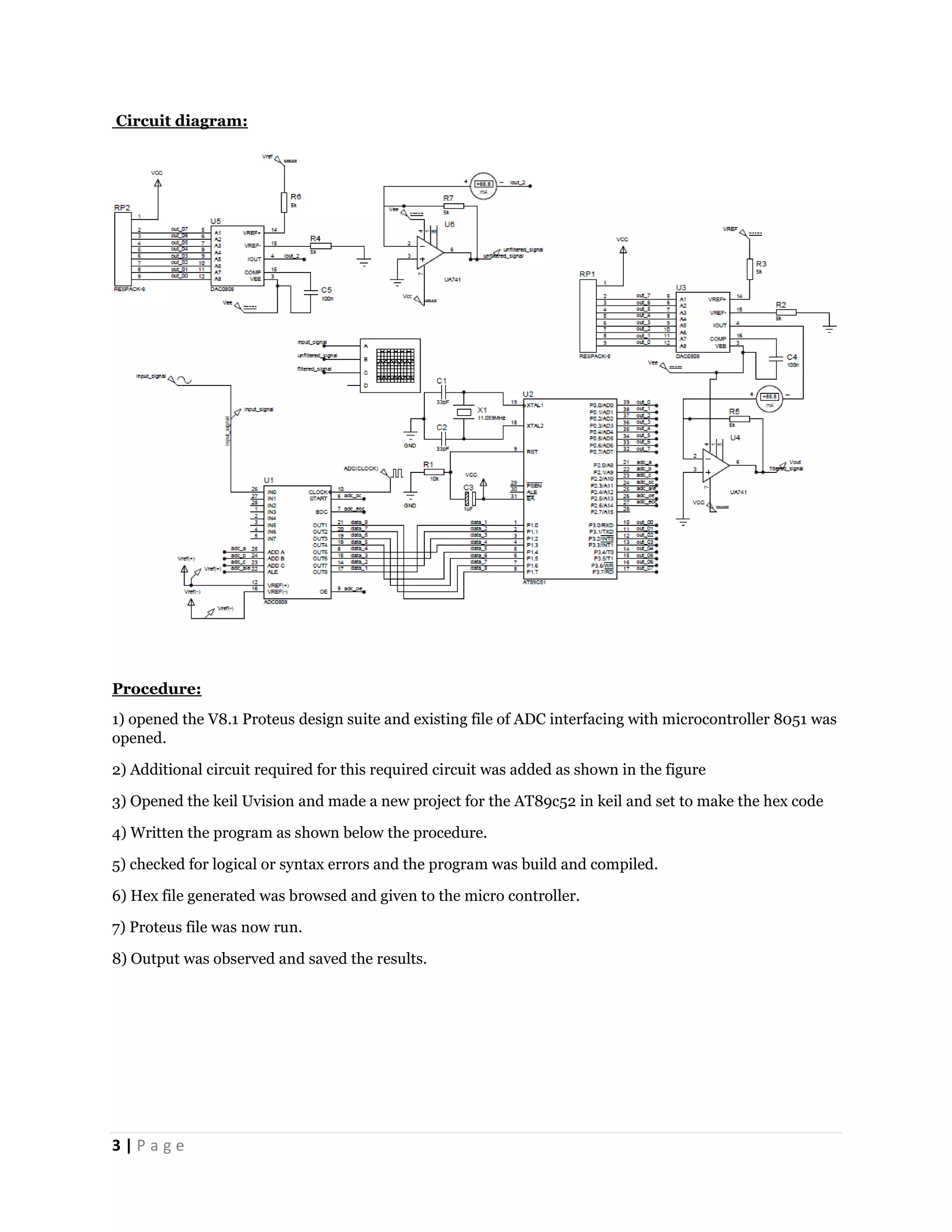
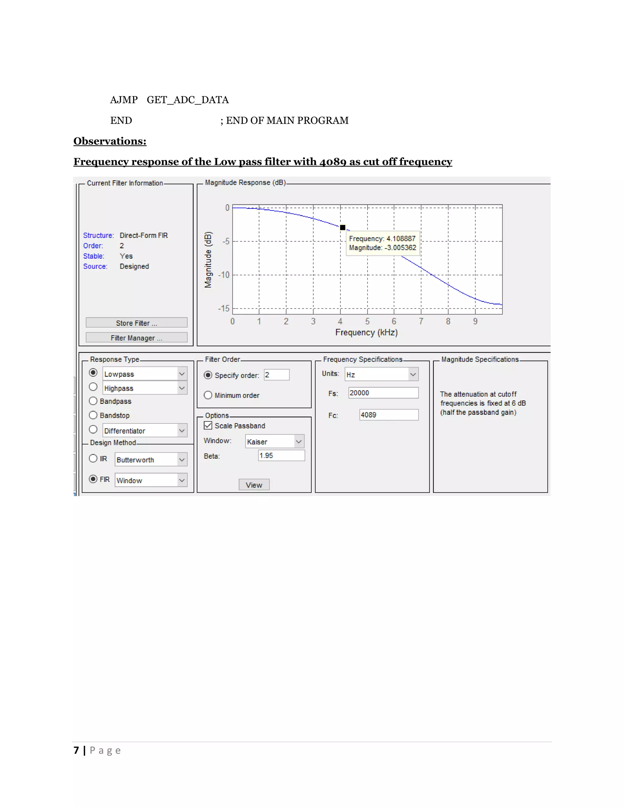
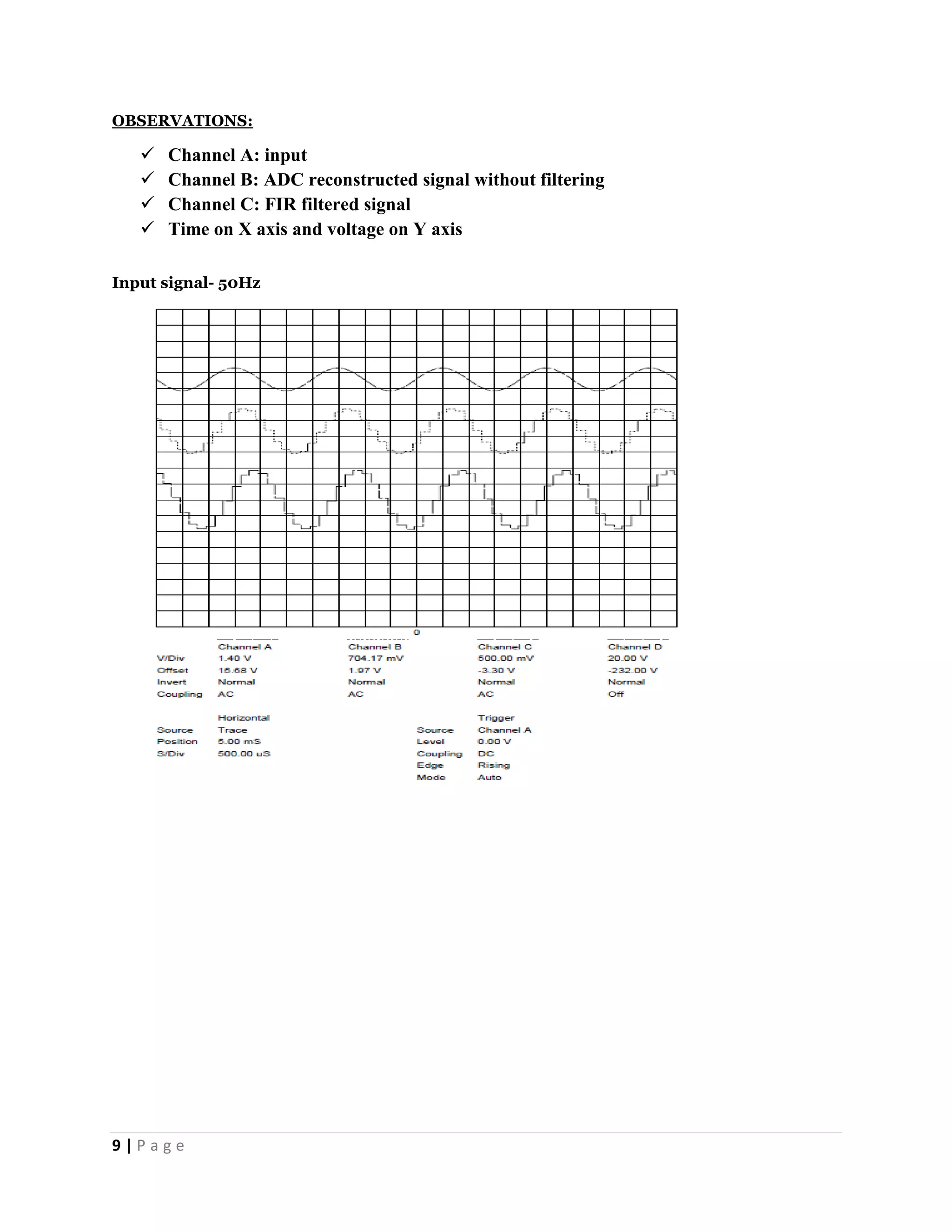
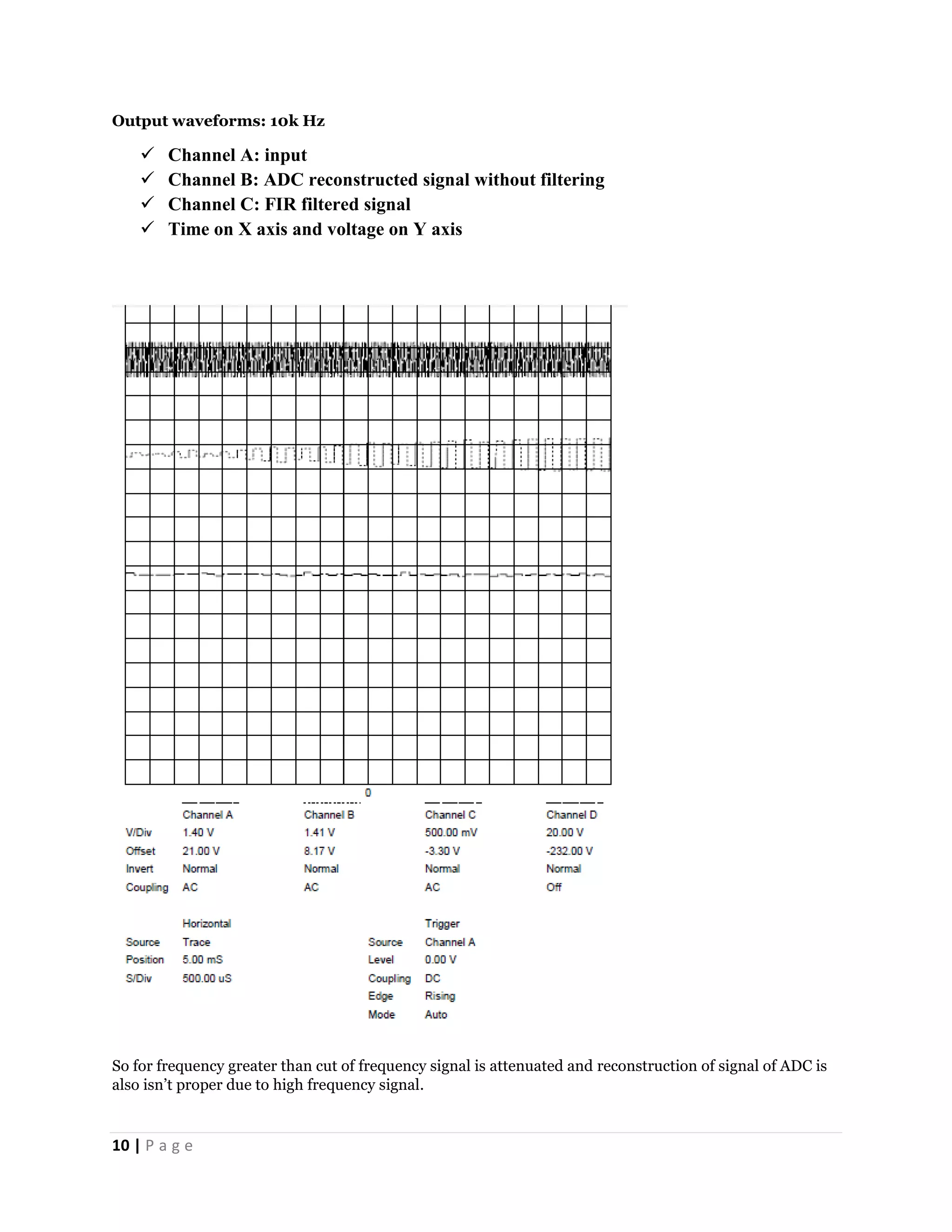
Guidance by
Dr. Supratim Gupta
Submitted by
Group 13
714ee4089 Aviral Tiwari
714ee4116 Nikhil Valiveti
714ee4122 Santhosh kumar
714ee4123 Abhishek Panda
REAL TIME SYSTEM LABORATORY
COURSE CODE: EE 481
LAB REPORT
1 | P a g e
EXPERIMENT 2
AIM: Design Low pass (LP) & Notch Filter with FIR structure of 2nd order
APPARTUS REQUIRED:
Name Specification quantity
Proteus software Version 8.1 -
Micro Controller AT89C51 1
ADC ADC0808 1
DAC DAC0808 2
Opamp IC 741 2
Resistors 10k, 5k , 8.2k,1k 5
Capacitors 30 pF, 0.1uF ,10uF 5
Digital Oscilloscope 0-10k 1
Crystal oscillator 11.0592MHz 1
DC voltage source 5V 5
AC voltage source V min -2.5 and V max- 2.5v ,
frequency 20Hz ,phase =0
1
Clock signal 500 KHz 1
Respack 9 terminal 2
Theory:
Digital Filter
A digital filter is a system that performs mathematical algorithm that operates on a digital input signal to
improve output signal for the purpose of achieving a filter objective such as: separation of signals that
have been combined, or restoration of signals that have been distorted. It refers to the specific hardware
and software routine that performs the filtering algorithm. Digital filter mostly operates on digitized
analog signals or just numbers, representing some variable, stored in a computer memory. A simplified
block diagram of a real-time digital filter with analog input and output signals, is given below. The band
limited analog signal is sampled periodically to generate a discrete time signal, which further quantized to
convert into series of digital samples x(n), n = 0,1,… and the digital processor implements the filtering
operation, mapping the input sequence x(n) into the output sequence y(n) in accordance with a
computational algorithm of the filter. The DAC converts the digitally filtered output into analog values.
2 | P a g e
Digital FIR filter
A Finite Impulse Response (FIR) filter is a type of signal processing filter whose impulse response ( or
response to any finite length input ) is of finite duration, because it settles to zero in finite time. The impulse
response of an Nth-order discrete-time FIR filter lasts for N+1 samples, and then dies to zero.
For a discrete-time FIR filter, the output is a weighted sum of the current and a finite number of previous
input values. The operation is described by the following equation, which defines the output
sequence y[n] in terms of its input sequence x[n] :
𝑌[𝑛] = 𝐵𝑜 ∗ 𝑥[𝑛] + 𝐵1 ∗ 𝑥[𝑛 − 1] + 𝐵2 ∗ 𝑥[𝑛 − 2] + ⋯ … . . 𝐵𝑁 ∗ 𝑥[𝑛 − 𝑁]
𝑦[𝑛] = ∑ 𝐵𝑖 ∗ 𝑥[𝑛 − 𝑖]𝑁
𝐼=0
 x[n] ----------- input signal
 y[n] ----------- output signal
 bi ----------- filter co-efficients
 N ----------- filter order
3 | P a g e
Circuit diagram:
Procedure:
1) opened the V8.1 Proteus design suite and existing file of ADC interfacing with microcontroller 8051 was
opened.
2) Additional circuit required for this required circuit was added as shown in the figure
3) Opened the keil Uvision and made a new project for the AT89c52 in keil and set to make the hex code
4) Written the program as shown below the procedure.
5) checked for logical or syntax errors and the program was build and compiled.
6) Hex file generated was browsed and given to the micro controller.
7) Proteus file was now run.
8) Output was observed and saved the results.
4 | P a g e
Assembly Code:
; ADC 0808 INTERFACING WITH ATMEL 89C51 UC
; WAIT TILL CONVERSION IS DONE
ADC_A BIT P2.0 ; DEFINE ADC PINS CONNECTED TO THE PINS OF MICROCONTROLLER
ADC_B BIT P2.1
ADC_C BIT P2.2
ADC_SC BIT P2.3
ADC_ALE BIT P2.4
ADC_OE BIT P2.5
ADC_EOC BIT P2.6
; FILTER COEFFICIENTS
K0 EQU 65
K1 EQU 125
K2 EQU 65
; DEFINE INPUT AND O/P PORTS
MYDATA EQU P1
OUT_DEQU P0
ORG 0000H ; SET START ADDRESS TO 0000H
SJMP MAIN ; JUMP TO MAIN PROGRAM
ORG 100H
MAIN:
MOV R0, #00H ; INITIALIZE THESE REGISTERS FOR STORING PARTIAL PRODUCTS
MOV R1, #00H
MOV R2, #00H
MOV R3, #00H
MOV R4, #00H
5 | P a g e
MOV R6, #00H ; TEMPORARY STORAGE FOR MSB AND LSB OF PARTIAL PRODUCTS
MOV R7, #00H
GET_ADC_DATA:
MOV MYDATA, #0FFH ; DEFINE MY_DATA AS I/P PORT
MOV OUT_D, #00H ; SET PORT 3 AS O/P PORT
MOV P3, #00H ; SET PORT 0 AS O/P PORT
SETB ADC_EOC
CLR ADC_OE
CLR ADC_ALE
CLR ADC_SC
CLR ADC_A ; FOR SELCTING INPUT PIN 1
CLR ADC_B
CLR ADC_C
SETB ADC_ALE
SETB ADC_SC
CLR ADC_ALE
CLR ADC_SC
WAIT: JNB ADC_EOC, WAIT ; WAIT TILL CONVERSION IS COMPLETE
SETB ADC_OE ; ENABLE THE OUTPUT PORT OF ADC
NOP
MOV A, P1 ; MOVE CONVERTED DATA FROM ADC TO ACCUMULATOR
MOV P3, A ; MOVE THE UNFILTERED SIGNAL TO PORT 3
CLR ADC_OE
SETB ADC_EOC
FILTER:
MOV R0, A ; FIRST ADC O/P SAMPLE MOVED TO RO
MOV B, #K0 ; KO MOVED TO B
6 | P a g e
MUL AB ; MULTIPLIED AB COZ OF TERM IN FILTER
MOV R7, A
MOV R6, B
MOV A, R1 ; SECOND ADC SAMPLE MOVED TO R1
MOV B, #K1 ; K1 MOVED TO B
MUL AB ; LOWER BYTE OF MULTIPLIED OUTPUT COPIED TO A
ADD A, R7 ; ADDING 1-2 TERMS LOWER BYTES OF DIGITAL FILTER EQUATION
MOV R7, A ; NOW R7 CONTAINS 2 TERMS SUM O/P LOWER BYTES
MOV A, B ; HIGHER BYTE IS COPIES TO A
ADDC A, R6
MOV R6, A
MOV A, R2
MOV B, #K2 ; K2 MOVED TO B
MUL AB ; MULTIPLIED PRODUCT STORED IN A
ADD A, R7 ; LOWER BYTE 3 TERMS SUMM IS STORED IN ACCUMULATOR
MOV R7, A ; R7 COTAINS THE SUM OF THE THREE TERMS LOWER BYTES
MOV A, B ;
ADDC A, R6
MOV R6, A
MOV OUT_D, A
NOP
SHIFT_ADC_DATA:
; SINCE THERE ARE ONLY 3 COEFFICIENTS R0, R1 ARE SHIFTED TO R1 AND R2
MOV A, R1
MOV R2, A ; MOVED THE TERM R0 TO R1
MOV A, R0
MOV R1, A ; MOVED THE TERM R1 TO R2
; ON EVERY LOOP R0 WILL BE THE OUTPUT OF A SAMPLE CONVERTED FROM ADC
7 | P a g e
AJMP GET_ADC_DATA
END ; END OF MAIN PROGRAM
Observations:
Frequency response of the Low pass filter with 4089 as cut off frequency
8 | P a g e
Frequency response of the Notch filter
9 | P a g e
OBSERVATIONS:
 Channel A: input
 Channel B: ADC reconstructed signal without filtering
 Channel C: FIR filtered signal
 Time on X axis and voltage on Y axis
Input signal- 50Hz
10 | P a g e
Output waveforms: 10k Hz
 Channel A: input
 Channel B: ADC reconstructed signal without filtering
 Channel C: FIR filtered signal
 Time on X axis and voltage on Y axis
So for frequency greater than cut of frequency signal is attenuated and reconstruction of signal of ADC is
also isn’t proper due to high frequency signal.
11 | P a g e
Result:
Since the cut off frequency is 4089Hz for the low pass filter this range of frequency signals aren’t
converted properly by ADC.
Even Notch filter was of 2nd order so the band stop filter’s quality factor is very low nearly zero. IIR filter
is preferred
Limitations:
FIR filter order must be preferably higher order for getting accurate results.
Cut off frequency of the filter must be lesser than Frequency limited by ADC
Conclusion:
Output filtered signal was similar to the input signal for low frequency signal and higher frequencies
amplitude is attenuated according to the frequency response.
References:
1. ADC0808, DAC0808 Data sheet
2. Muhammad Ali Mazidi, Janice GillispieMazidi, and Rolin D. McKinlay, “The 8051 microcontroller
and embedded systems,” Vol. 1. Upper Saddle River, NJ, USA, Prentice hall, 2000.
12 | P a g e

Low pass digital filter using FIR structure of 2nd order

  • 1.
    Guidance by Dr. SupratimGupta Submitted by Group 13 714ee4089 Aviral Tiwari 714ee4116 Nikhil Valiveti 714ee4122 Santhosh kumar 714ee4123 Abhishek Panda REAL TIME SYSTEM LABORATORY COURSE CODE: EE 481 LAB REPORT
  • 2.
    1 | Pa g e EXPERIMENT 2 AIM: Design Low pass (LP) & Notch Filter with FIR structure of 2nd order APPARTUS REQUIRED: Name Specification quantity Proteus software Version 8.1 - Micro Controller AT89C51 1 ADC ADC0808 1 DAC DAC0808 2 Opamp IC 741 2 Resistors 10k, 5k , 8.2k,1k 5 Capacitors 30 pF, 0.1uF ,10uF 5 Digital Oscilloscope 0-10k 1 Crystal oscillator 11.0592MHz 1 DC voltage source 5V 5 AC voltage source V min -2.5 and V max- 2.5v , frequency 20Hz ,phase =0 1 Clock signal 500 KHz 1 Respack 9 terminal 2 Theory: Digital Filter A digital filter is a system that performs mathematical algorithm that operates on a digital input signal to improve output signal for the purpose of achieving a filter objective such as: separation of signals that have been combined, or restoration of signals that have been distorted. It refers to the specific hardware and software routine that performs the filtering algorithm. Digital filter mostly operates on digitized analog signals or just numbers, representing some variable, stored in a computer memory. A simplified block diagram of a real-time digital filter with analog input and output signals, is given below. The band limited analog signal is sampled periodically to generate a discrete time signal, which further quantized to convert into series of digital samples x(n), n = 0,1,… and the digital processor implements the filtering operation, mapping the input sequence x(n) into the output sequence y(n) in accordance with a computational algorithm of the filter. The DAC converts the digitally filtered output into analog values.
  • 3.
    2 | Pa g e Digital FIR filter A Finite Impulse Response (FIR) filter is a type of signal processing filter whose impulse response ( or response to any finite length input ) is of finite duration, because it settles to zero in finite time. The impulse response of an Nth-order discrete-time FIR filter lasts for N+1 samples, and then dies to zero. For a discrete-time FIR filter, the output is a weighted sum of the current and a finite number of previous input values. The operation is described by the following equation, which defines the output sequence y[n] in terms of its input sequence x[n] : 𝑌[𝑛] = 𝐵𝑜 ∗ 𝑥[𝑛] + 𝐵1 ∗ 𝑥[𝑛 − 1] + 𝐵2 ∗ 𝑥[𝑛 − 2] + ⋯ … . . 𝐵𝑁 ∗ 𝑥[𝑛 − 𝑁] 𝑦[𝑛] = ∑ 𝐵𝑖 ∗ 𝑥[𝑛 − 𝑖]𝑁 𝐼=0  x[n] ----------- input signal  y[n] ----------- output signal  bi ----------- filter co-efficients  N ----------- filter order
  • 4.
    3 | Pa g e Circuit diagram: Procedure: 1) opened the V8.1 Proteus design suite and existing file of ADC interfacing with microcontroller 8051 was opened. 2) Additional circuit required for this required circuit was added as shown in the figure 3) Opened the keil Uvision and made a new project for the AT89c52 in keil and set to make the hex code 4) Written the program as shown below the procedure. 5) checked for logical or syntax errors and the program was build and compiled. 6) Hex file generated was browsed and given to the micro controller. 7) Proteus file was now run. 8) Output was observed and saved the results.
  • 5.
    4 | Pa g e Assembly Code: ; ADC 0808 INTERFACING WITH ATMEL 89C51 UC ; WAIT TILL CONVERSION IS DONE ADC_A BIT P2.0 ; DEFINE ADC PINS CONNECTED TO THE PINS OF MICROCONTROLLER ADC_B BIT P2.1 ADC_C BIT P2.2 ADC_SC BIT P2.3 ADC_ALE BIT P2.4 ADC_OE BIT P2.5 ADC_EOC BIT P2.6 ; FILTER COEFFICIENTS K0 EQU 65 K1 EQU 125 K2 EQU 65 ; DEFINE INPUT AND O/P PORTS MYDATA EQU P1 OUT_DEQU P0 ORG 0000H ; SET START ADDRESS TO 0000H SJMP MAIN ; JUMP TO MAIN PROGRAM ORG 100H MAIN: MOV R0, #00H ; INITIALIZE THESE REGISTERS FOR STORING PARTIAL PRODUCTS MOV R1, #00H MOV R2, #00H MOV R3, #00H MOV R4, #00H
  • 6.
    5 | Pa g e MOV R6, #00H ; TEMPORARY STORAGE FOR MSB AND LSB OF PARTIAL PRODUCTS MOV R7, #00H GET_ADC_DATA: MOV MYDATA, #0FFH ; DEFINE MY_DATA AS I/P PORT MOV OUT_D, #00H ; SET PORT 3 AS O/P PORT MOV P3, #00H ; SET PORT 0 AS O/P PORT SETB ADC_EOC CLR ADC_OE CLR ADC_ALE CLR ADC_SC CLR ADC_A ; FOR SELCTING INPUT PIN 1 CLR ADC_B CLR ADC_C SETB ADC_ALE SETB ADC_SC CLR ADC_ALE CLR ADC_SC WAIT: JNB ADC_EOC, WAIT ; WAIT TILL CONVERSION IS COMPLETE SETB ADC_OE ; ENABLE THE OUTPUT PORT OF ADC NOP MOV A, P1 ; MOVE CONVERTED DATA FROM ADC TO ACCUMULATOR MOV P3, A ; MOVE THE UNFILTERED SIGNAL TO PORT 3 CLR ADC_OE SETB ADC_EOC FILTER: MOV R0, A ; FIRST ADC O/P SAMPLE MOVED TO RO MOV B, #K0 ; KO MOVED TO B
  • 7.
    6 | Pa g e MUL AB ; MULTIPLIED AB COZ OF TERM IN FILTER MOV R7, A MOV R6, B MOV A, R1 ; SECOND ADC SAMPLE MOVED TO R1 MOV B, #K1 ; K1 MOVED TO B MUL AB ; LOWER BYTE OF MULTIPLIED OUTPUT COPIED TO A ADD A, R7 ; ADDING 1-2 TERMS LOWER BYTES OF DIGITAL FILTER EQUATION MOV R7, A ; NOW R7 CONTAINS 2 TERMS SUM O/P LOWER BYTES MOV A, B ; HIGHER BYTE IS COPIES TO A ADDC A, R6 MOV R6, A MOV A, R2 MOV B, #K2 ; K2 MOVED TO B MUL AB ; MULTIPLIED PRODUCT STORED IN A ADD A, R7 ; LOWER BYTE 3 TERMS SUMM IS STORED IN ACCUMULATOR MOV R7, A ; R7 COTAINS THE SUM OF THE THREE TERMS LOWER BYTES MOV A, B ; ADDC A, R6 MOV R6, A MOV OUT_D, A NOP SHIFT_ADC_DATA: ; SINCE THERE ARE ONLY 3 COEFFICIENTS R0, R1 ARE SHIFTED TO R1 AND R2 MOV A, R1 MOV R2, A ; MOVED THE TERM R0 TO R1 MOV A, R0 MOV R1, A ; MOVED THE TERM R1 TO R2 ; ON EVERY LOOP R0 WILL BE THE OUTPUT OF A SAMPLE CONVERTED FROM ADC
  • 8.
    7 | Pa g e AJMP GET_ADC_DATA END ; END OF MAIN PROGRAM Observations: Frequency response of the Low pass filter with 4089 as cut off frequency
  • 9.
    8 | Pa g e Frequency response of the Notch filter
  • 10.
    9 | Pa g e OBSERVATIONS:  Channel A: input  Channel B: ADC reconstructed signal without filtering  Channel C: FIR filtered signal  Time on X axis and voltage on Y axis Input signal- 50Hz
  • 11.
    10 | Pa g e Output waveforms: 10k Hz  Channel A: input  Channel B: ADC reconstructed signal without filtering  Channel C: FIR filtered signal  Time on X axis and voltage on Y axis So for frequency greater than cut of frequency signal is attenuated and reconstruction of signal of ADC is also isn’t proper due to high frequency signal.
  • 12.
    11 | Pa g e Result: Since the cut off frequency is 4089Hz for the low pass filter this range of frequency signals aren’t converted properly by ADC. Even Notch filter was of 2nd order so the band stop filter’s quality factor is very low nearly zero. IIR filter is preferred Limitations: FIR filter order must be preferably higher order for getting accurate results. Cut off frequency of the filter must be lesser than Frequency limited by ADC Conclusion: Output filtered signal was similar to the input signal for low frequency signal and higher frequencies amplitude is attenuated according to the frequency response. References: 1. ADC0808, DAC0808 Data sheet 2. Muhammad Ali Mazidi, Janice GillispieMazidi, and Rolin D. McKinlay, “The 8051 microcontroller and embedded systems,” Vol. 1. Upper Saddle River, NJ, USA, Prentice hall, 2000.
  • 13.
    12 | Pa g e