Implementation of a Sigma Delta Analog to
Digital Converter in an RTAX FPGA
MAPLD
September 1, 2009
Doug Cornelsen
Electrical Engineering
Bristol Aerospace Limited
Winnipeg, Manitoba, Canada
doug.cornelsen@magellan.aero
Revision: A
Date: Sept 1, 2009
Page: 2
Presentation Overview
• This presentation focuses on the FPGA portion of the design, not
the portion external to the FPGA
– Design Motivation and Constraints
– Design Flow (MATLAB->Simulink->Libero->Identify)
– Filter Design
– Preliminary Test Results
Revision: A
Date: Sept 1, 2009
Page: 3
Design Motivation
• The concept of using an FPGA based ADC stemmed from:
– A desire to acquire 10-bit (accuracy) low rate telemetry (<1 KHz) utilizing
existing components (RTAX250S)
– The motivation to have a design which can be replicated with a cost less than
a traditional radiation hardened ADC
• Assuming surplus FPGA resources are available (in a FPGA already
designed into circuitry) only need to add a few external components
• Existing design requires at least RTAX250S to meet combinational and
sequential requirements
– Trade of RTAX250S with radiation hardened ADC versus RTAX250S
and embedded sigma delta ADC
• Radiation hardened ADC less power but more cost
• The application for such a converter is primarily for on board
diagnostics and monitoring.
Revision: A
Date: Sept 1, 2009
Page: 4
Design Constraints
• > 10 bits accuracy (12 desired)
• < 25% utilization of combination and sequential resources of
RTAX250
• All block ram available for use
• >1 KHz sampling rate
– When input held on the same analog multiplexer input
• >100 Hz sampling rate
– When analog multiplexer cycled though various inputs
– Need to allow filter memory to “flush” when new input is muxed in
• FIR filter memory contains values from previous inputs these must be
overwritten with values from the new input
• Automated process for filter coefficient generation
• Ability to compare and simulate “golden” MATLAB filter reference
with hand coded optimized version
Revision: A
Date: Sept 1, 2009
Page: 5
Sigma Delta ADC Overview
• A sigma delta ADC does not digitize the analog signal at the
Nyquist rate
• Rather it over samples the analog signal
– Samples at a lower precision but higher rate (e.g 16, 32 …)
– Most sigma delta ADC are based on a 1-bit A/D
• Contains two main components a modulator and a decimating
filter
• The output of the modulator is a bit stream with a one’s density
proportional to the magnitude of the input
• The 1-bit ADC stream that is generated is filtered and decimated
(by the decimating filter) back down to a Nyquist rate of n-bit
precision samples
• The result is a n-bit conversion
Revision: A
Date: Sept 1, 2009
Page: 6
Filter Design
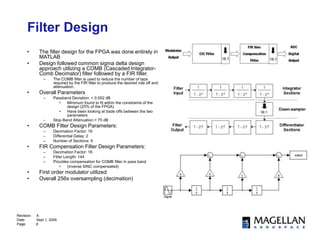
• The filter design for the FPGA was done entirely in
MATLAB
• Design followed common sigma delta design
approach utilizing a COMB (Cascaded Integrator-
Comb Decimator) filter followed by a FIR filter.
– The COMB filter is used to reduce the number of taps
required by the FIR filter to produce the desired role off and
attenuation.
• Overall Parameters
– Passband Deviation: < 0.002 dB
• Minimum found to fit within the constraints of the
design (25% of the FPGA)
• Have been looking at trade offs between the two
parameters
– Stop Band Attenuation > 75 dB
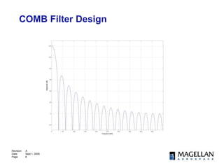
• COMB Filter Design Parameters:
– Decimation Factor: 16
– Differential Delay: 2
– Number of Sections: 4
• FIR Compensation Filter Design Parameters:
– Decimation Factor: 16
– Filter Length: 144
– Provides compensation for COMB filter in pass band
• (inverse SINC compensated)
• First order modulator utilized
• Overall 256x oversampling (decimation)
Revision: A
Date: Sept 1, 2009
Page: 7
Filter Design
• Design Parameters somewhat follow
MATLAB 16-Bit (Sigma Delta) ADC
example:
– Pass Band Ripple: 0.006 dB
– Stop Band Attenuation: 90 dB
– Fourth Order Modulator, 64x oversampling
(decimating)
– MATLAB example found at:
http://www.mathworks.com/company/newsle
tters/digest/2007/sept/sigmadelta.html
• 10.5 bits is about the best possible
result obtainable with first order
modulator (@ 256x oversampling)
– SNR = 6.02N+1.76dB for an N bit analog to
digital converter
– Modulator is essentially the limiting factor
Revision: A
Date: Sept 1, 2009
Page: 8
COMB Filter Design
Revision: A
Date: Sept 1, 2009
Page: 9
Cascaded Filter Design (COMB+FIR)
Revision: A
Date: Sept 1, 2009
Page: 10
Simulink Simulation
Revision: A
Date: Sept 1, 2009
Page: 11
MATLAB .vhd Synthesis Results (RTAX)
• MATLAB COMB
• Target Part: rtax250s_cqfp208-1
Combinational Cells: 538 of 2816 (19%)
Sequential Cells: 302 of 1408 (21%)
Total Cells: 840 of 4224 (20%)
• MATLAB FIR (~144 multipliers, one input fixed on each,
basically performs one large cascaded multiplication)
• Target Part: rtax250s_cqfp208-1
Combinational Cells: 16030 of 2816 (569%)
Sequential Cells: 2852 of 1408 (203%)
Total Cells: 18882 of 4224 (448%)
Revision: A
Date: Sept 1, 2009
Page: 12
Hand Coded .vhd Synthesis Results (RTAX)
Comb Modifications
1. Replace registers in differentiator section with (TMR’d) block ram instead of registers.
2. Modify the design to share adders in differentiator section.
Target Part: rtax250s_cqfp208-1
Combinational Cells: 270 of 2816 (10%)
Sequential Cells: 105 of 1408 (7%)
Total Cells: 375 of 4224 (9%)
FIR Modifications:
1. Replace many multipliers with fixed coefficients with single multiplier (serial signed multiplier)
and ROM
• Single large cascaded multiplication replaced with multiplications performed as results arrive
2. Store temporary results in (TMR’d) block ram instead of shift registers
• Each block ram location is written over every 2.5 ms
3. After reset force input of multiplier to default values when out of RAM is undefined.
4. Run multiplier 10x faster than modulator input to allow enough time for math operations
(Modulator: 1 MHz, Math: 10 MHz)
• 1 MHz/256 = 3906.25 samples/sec
Target Part: rtax250s_cqfp208-1
Combinational Cells: 404 of 2816 (14%)
Sequential Cells: 193 of 1408 (14%)
Total Cells: 597 of 4224 (15%)
Revision: A
Date: Sept 1, 2009
Page: 13
PA3 Bench Testing Setup:
Analog
Mux
0V
1.5V
3.3V
User Input
Function
Generator
or Precision
Source
Modulator
PA3 FPGA
(CoreMP7
Dev Kit)
UART
PC
(Capture
Sample
Packets)
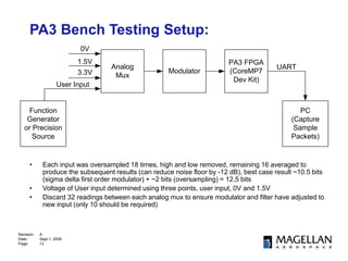
• Each input was oversampled 18 times, high and low removed, remaining 16 averaged to
produce the subsequent results (can reduce noise floor by -12 dB), best case result ~10.5 bits
(sigma delta first order modulator) + ~2 bits (oversampling) = 12.5 bits
• Voltage of User input determined using three points, user input, 0V and 1.5V
• Discard 32 readings between each analog mux to ensure modulator and filter have adjusted to
new input (only 10 should be required)
Revision: A
Date: Sept 1, 2009
Page: 14
PA3 Bench Testing Results: Accuracy
Estimated Accuracy
9
9.5
10
10.5
11
11.5
12
12.5
13
13.5
14
0 500 1000 1500 2000 2500 3000 3500
Input Voltage (mV)
Estimated
Accuracy
(bits)
Estimated Accuracy (Best Fit)
9
9.5
10
10.5
11
11.5
12
12.5
13
13.5
14
0 500 1000 1500 2000 2500 3000 3500
Input Voltage (mV)
Estimated
Accuracy
(bits)
Revision: A
Date: Sept 1, 2009
Page: 15
PA3 Bench Testing Results: Delta
Mean Delta From Input
-1.8
-1.6
-1.4
-1.2
-1
-0.8
-0.6
-0.4
-0.2
0
0 500 1000 1500 2000 2500 3000 3500
Input (mV)
Delta
(mV)
• Linear delta caused by slight offset error in 1.5V calibration point, once
fixed should result in at least ½ bit performance improvement for voltages
above 2.0V
Revision: A
Date: Sept 1, 2009
Page: 16
PA3 Bench Testing Results: Standard Deviation
Standard Deviation
0
0.01
0.02
0.03
0.04
0.05
0.06
0.07
0.08
0.09
0.1
0 500 1000 1500 2000 2500 3000 3500
Input Voltage (mV)
Standard
Deviation
(mV)
3 Sigma (99.7%)
0
0.05
0.1
0.15
0.2
0.25
0.3
0 500 1000 1500 2000 2500 3000 3500
Input Voltage (mV)
3
Sigma
(mV)
Revision: A
Date: Sept 1, 2009
Page: 17
PA3 Bench Testing Results: 2 Hour Test
• 131,072 samples @ 500 mV
Revision: A
Date: Sept 1, 2009
Page: 18
PA3 Bench Testing Results: Sinusoidal Input
– SNR = 6.02N+1.76dB for an N bit analog to digital converter
– Input 0-2V 3 Hz sinusoid, 70 dB, N = 11.33 bits, 32768 points for input to FFT
Revision: A
Date: Sept 1, 2009
Page: 19
Future Plans
1. Prototype in AX250
2. Test Performance Over Temperature Range
3. Utilize IEEE standard for determining ADC performance
Conclusion
1. FPGA based Sigma Delta has meet design goals and proven viable
enough to proceed to next level of prototyping and verification

02_Cornelsen_Doug_mapld09_pres_1.ppt

  • 1.
    Implementation of aSigma Delta Analog to Digital Converter in an RTAX FPGA MAPLD September 1, 2009 Doug Cornelsen Electrical Engineering Bristol Aerospace Limited Winnipeg, Manitoba, Canada doug.cornelsen@magellan.aero
  • 2.
    Revision: A Date: Sept1, 2009 Page: 2 Presentation Overview • This presentation focuses on the FPGA portion of the design, not the portion external to the FPGA – Design Motivation and Constraints – Design Flow (MATLAB->Simulink->Libero->Identify) – Filter Design – Preliminary Test Results
  • 3.
    Revision: A Date: Sept1, 2009 Page: 3 Design Motivation • The concept of using an FPGA based ADC stemmed from: – A desire to acquire 10-bit (accuracy) low rate telemetry (<1 KHz) utilizing existing components (RTAX250S) – The motivation to have a design which can be replicated with a cost less than a traditional radiation hardened ADC • Assuming surplus FPGA resources are available (in a FPGA already designed into circuitry) only need to add a few external components • Existing design requires at least RTAX250S to meet combinational and sequential requirements – Trade of RTAX250S with radiation hardened ADC versus RTAX250S and embedded sigma delta ADC • Radiation hardened ADC less power but more cost • The application for such a converter is primarily for on board diagnostics and monitoring.
  • 4.
    Revision: A Date: Sept1, 2009 Page: 4 Design Constraints • > 10 bits accuracy (12 desired) • < 25% utilization of combination and sequential resources of RTAX250 • All block ram available for use • >1 KHz sampling rate – When input held on the same analog multiplexer input • >100 Hz sampling rate – When analog multiplexer cycled though various inputs – Need to allow filter memory to “flush” when new input is muxed in • FIR filter memory contains values from previous inputs these must be overwritten with values from the new input • Automated process for filter coefficient generation • Ability to compare and simulate “golden” MATLAB filter reference with hand coded optimized version
  • 5.
    Revision: A Date: Sept1, 2009 Page: 5 Sigma Delta ADC Overview • A sigma delta ADC does not digitize the analog signal at the Nyquist rate • Rather it over samples the analog signal – Samples at a lower precision but higher rate (e.g 16, 32 …) – Most sigma delta ADC are based on a 1-bit A/D • Contains two main components a modulator and a decimating filter • The output of the modulator is a bit stream with a one’s density proportional to the magnitude of the input • The 1-bit ADC stream that is generated is filtered and decimated (by the decimating filter) back down to a Nyquist rate of n-bit precision samples • The result is a n-bit conversion
  • 6.
    Revision: A Date: Sept1, 2009 Page: 6 Filter Design • The filter design for the FPGA was done entirely in MATLAB • Design followed common sigma delta design approach utilizing a COMB (Cascaded Integrator- Comb Decimator) filter followed by a FIR filter. – The COMB filter is used to reduce the number of taps required by the FIR filter to produce the desired role off and attenuation. • Overall Parameters – Passband Deviation: < 0.002 dB • Minimum found to fit within the constraints of the design (25% of the FPGA) • Have been looking at trade offs between the two parameters – Stop Band Attenuation > 75 dB • COMB Filter Design Parameters: – Decimation Factor: 16 – Differential Delay: 2 – Number of Sections: 4 • FIR Compensation Filter Design Parameters: – Decimation Factor: 16 – Filter Length: 144 – Provides compensation for COMB filter in pass band • (inverse SINC compensated) • First order modulator utilized • Overall 256x oversampling (decimation)
  • 7.
    Revision: A Date: Sept1, 2009 Page: 7 Filter Design • Design Parameters somewhat follow MATLAB 16-Bit (Sigma Delta) ADC example: – Pass Band Ripple: 0.006 dB – Stop Band Attenuation: 90 dB – Fourth Order Modulator, 64x oversampling (decimating) – MATLAB example found at: http://www.mathworks.com/company/newsle tters/digest/2007/sept/sigmadelta.html • 10.5 bits is about the best possible result obtainable with first order modulator (@ 256x oversampling) – SNR = 6.02N+1.76dB for an N bit analog to digital converter – Modulator is essentially the limiting factor
  • 8.
    Revision: A Date: Sept1, 2009 Page: 8 COMB Filter Design
  • 9.
    Revision: A Date: Sept1, 2009 Page: 9 Cascaded Filter Design (COMB+FIR)
  • 10.
    Revision: A Date: Sept1, 2009 Page: 10 Simulink Simulation
  • 11.
    Revision: A Date: Sept1, 2009 Page: 11 MATLAB .vhd Synthesis Results (RTAX) • MATLAB COMB • Target Part: rtax250s_cqfp208-1 Combinational Cells: 538 of 2816 (19%) Sequential Cells: 302 of 1408 (21%) Total Cells: 840 of 4224 (20%) • MATLAB FIR (~144 multipliers, one input fixed on each, basically performs one large cascaded multiplication) • Target Part: rtax250s_cqfp208-1 Combinational Cells: 16030 of 2816 (569%) Sequential Cells: 2852 of 1408 (203%) Total Cells: 18882 of 4224 (448%)
  • 12.
    Revision: A Date: Sept1, 2009 Page: 12 Hand Coded .vhd Synthesis Results (RTAX) Comb Modifications 1. Replace registers in differentiator section with (TMR’d) block ram instead of registers. 2. Modify the design to share adders in differentiator section. Target Part: rtax250s_cqfp208-1 Combinational Cells: 270 of 2816 (10%) Sequential Cells: 105 of 1408 (7%) Total Cells: 375 of 4224 (9%) FIR Modifications: 1. Replace many multipliers with fixed coefficients with single multiplier (serial signed multiplier) and ROM • Single large cascaded multiplication replaced with multiplications performed as results arrive 2. Store temporary results in (TMR’d) block ram instead of shift registers • Each block ram location is written over every 2.5 ms 3. After reset force input of multiplier to default values when out of RAM is undefined. 4. Run multiplier 10x faster than modulator input to allow enough time for math operations (Modulator: 1 MHz, Math: 10 MHz) • 1 MHz/256 = 3906.25 samples/sec Target Part: rtax250s_cqfp208-1 Combinational Cells: 404 of 2816 (14%) Sequential Cells: 193 of 1408 (14%) Total Cells: 597 of 4224 (15%)
  • 13.
    Revision: A Date: Sept1, 2009 Page: 13 PA3 Bench Testing Setup: Analog Mux 0V 1.5V 3.3V User Input Function Generator or Precision Source Modulator PA3 FPGA (CoreMP7 Dev Kit) UART PC (Capture Sample Packets) • Each input was oversampled 18 times, high and low removed, remaining 16 averaged to produce the subsequent results (can reduce noise floor by -12 dB), best case result ~10.5 bits (sigma delta first order modulator) + ~2 bits (oversampling) = 12.5 bits • Voltage of User input determined using three points, user input, 0V and 1.5V • Discard 32 readings between each analog mux to ensure modulator and filter have adjusted to new input (only 10 should be required)
  • 14.
    Revision: A Date: Sept1, 2009 Page: 14 PA3 Bench Testing Results: Accuracy Estimated Accuracy 9 9.5 10 10.5 11 11.5 12 12.5 13 13.5 14 0 500 1000 1500 2000 2500 3000 3500 Input Voltage (mV) Estimated Accuracy (bits) Estimated Accuracy (Best Fit) 9 9.5 10 10.5 11 11.5 12 12.5 13 13.5 14 0 500 1000 1500 2000 2500 3000 3500 Input Voltage (mV) Estimated Accuracy (bits)
  • 15.
    Revision: A Date: Sept1, 2009 Page: 15 PA3 Bench Testing Results: Delta Mean Delta From Input -1.8 -1.6 -1.4 -1.2 -1 -0.8 -0.6 -0.4 -0.2 0 0 500 1000 1500 2000 2500 3000 3500 Input (mV) Delta (mV) • Linear delta caused by slight offset error in 1.5V calibration point, once fixed should result in at least ½ bit performance improvement for voltages above 2.0V
  • 16.
    Revision: A Date: Sept1, 2009 Page: 16 PA3 Bench Testing Results: Standard Deviation Standard Deviation 0 0.01 0.02 0.03 0.04 0.05 0.06 0.07 0.08 0.09 0.1 0 500 1000 1500 2000 2500 3000 3500 Input Voltage (mV) Standard Deviation (mV) 3 Sigma (99.7%) 0 0.05 0.1 0.15 0.2 0.25 0.3 0 500 1000 1500 2000 2500 3000 3500 Input Voltage (mV) 3 Sigma (mV)
  • 17.
    Revision: A Date: Sept1, 2009 Page: 17 PA3 Bench Testing Results: 2 Hour Test • 131,072 samples @ 500 mV
  • 18.
    Revision: A Date: Sept1, 2009 Page: 18 PA3 Bench Testing Results: Sinusoidal Input – SNR = 6.02N+1.76dB for an N bit analog to digital converter – Input 0-2V 3 Hz sinusoid, 70 dB, N = 11.33 bits, 32768 points for input to FFT
  • 19.
    Revision: A Date: Sept1, 2009 Page: 19 Future Plans 1. Prototype in AX250 2. Test Performance Over Temperature Range 3. Utilize IEEE standard for determining ADC performance Conclusion 1. FPGA based Sigma Delta has meet design goals and proven viable enough to proceed to next level of prototyping and verification