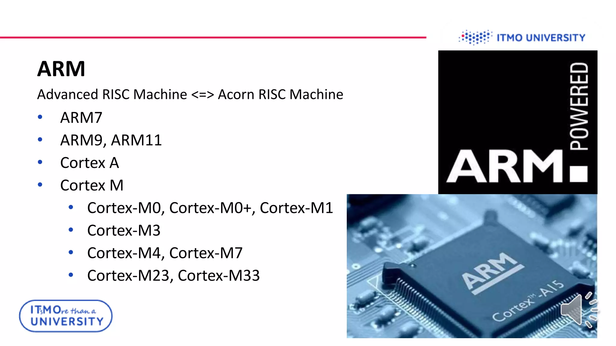
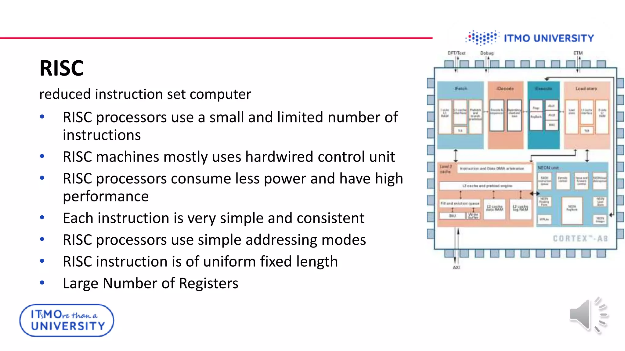
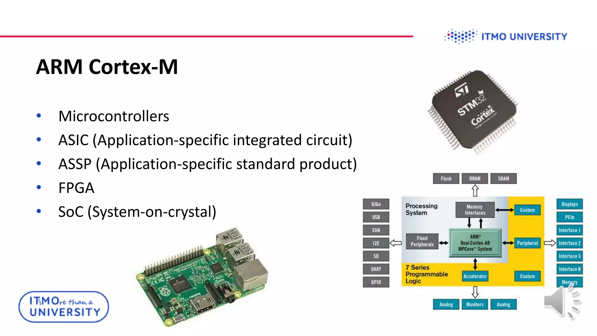
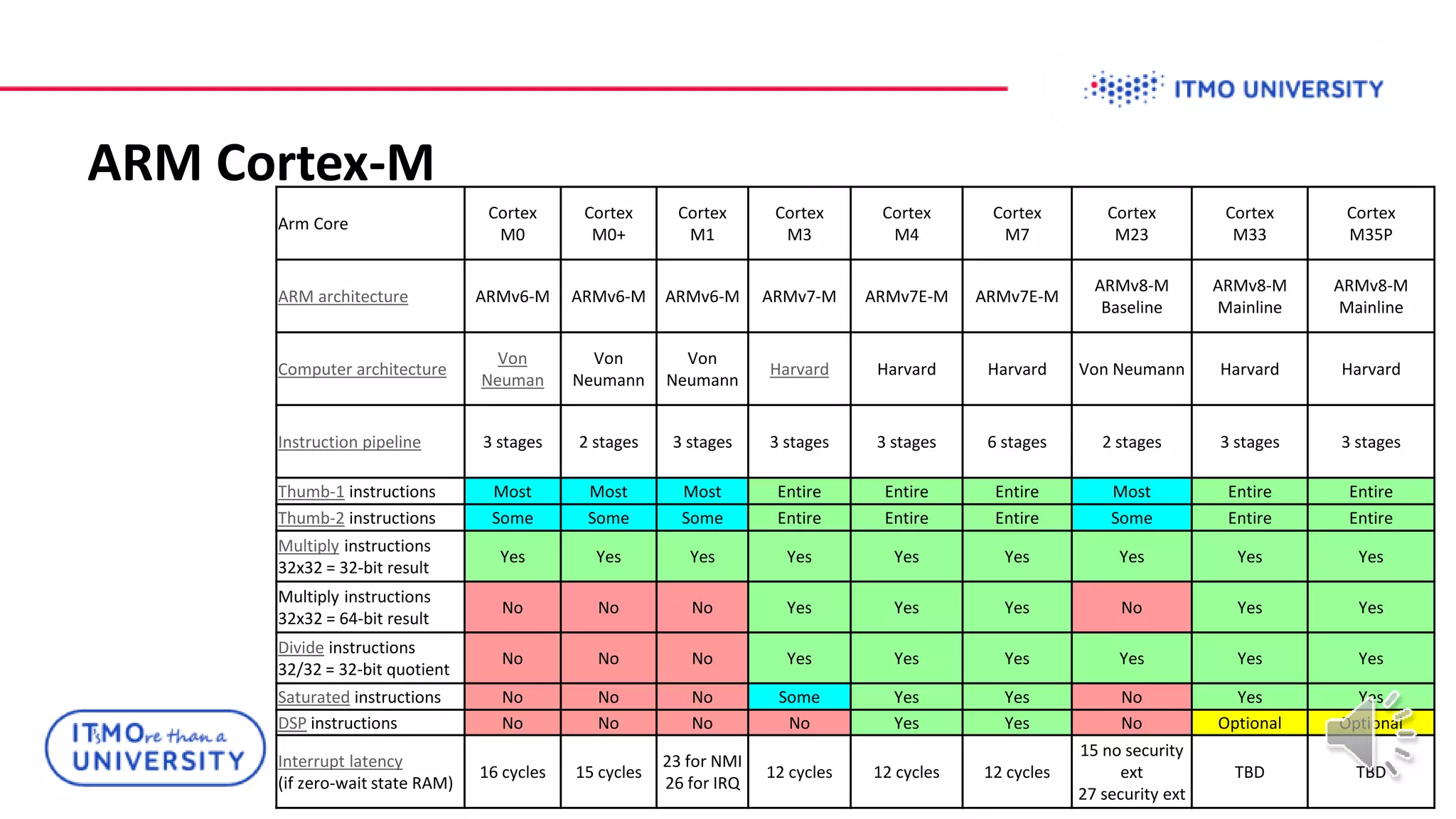
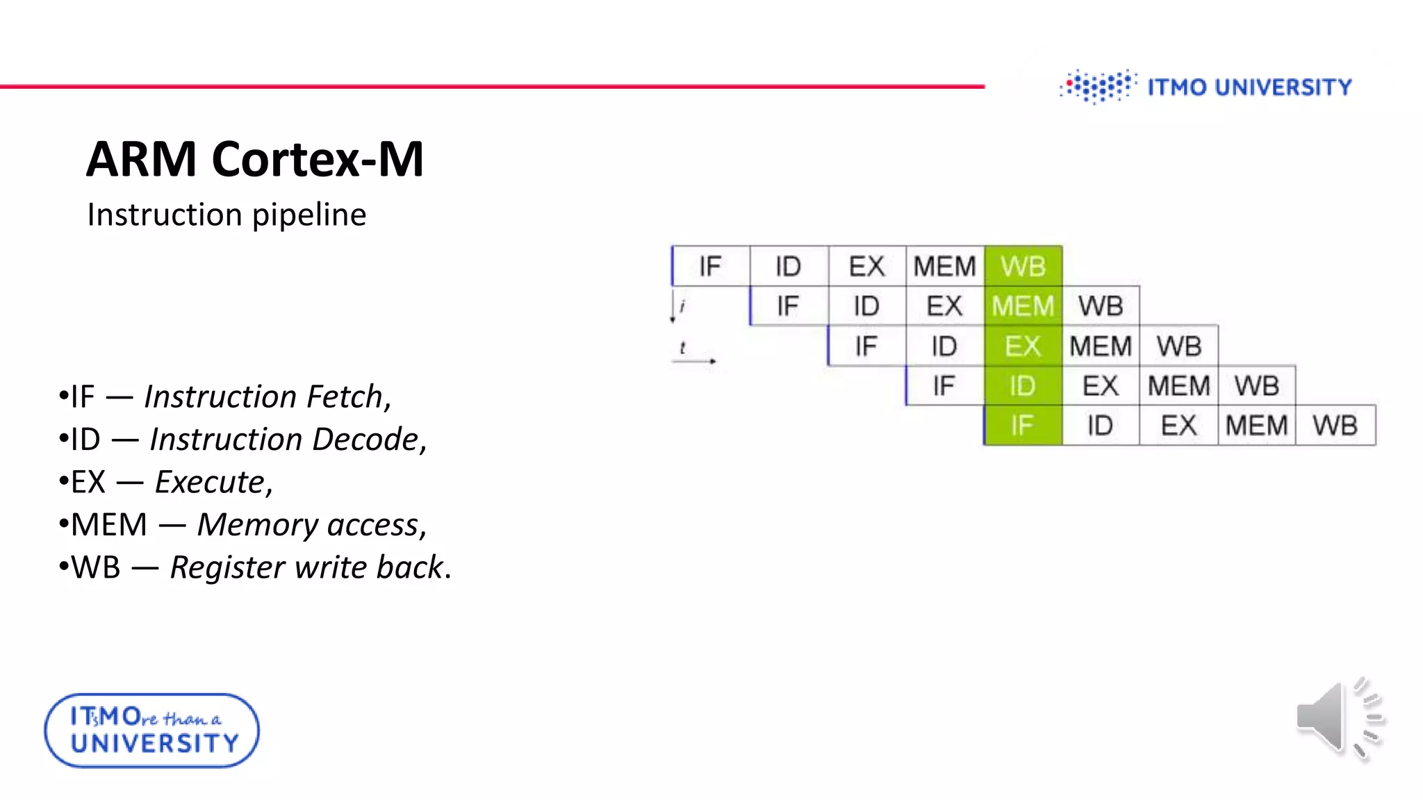
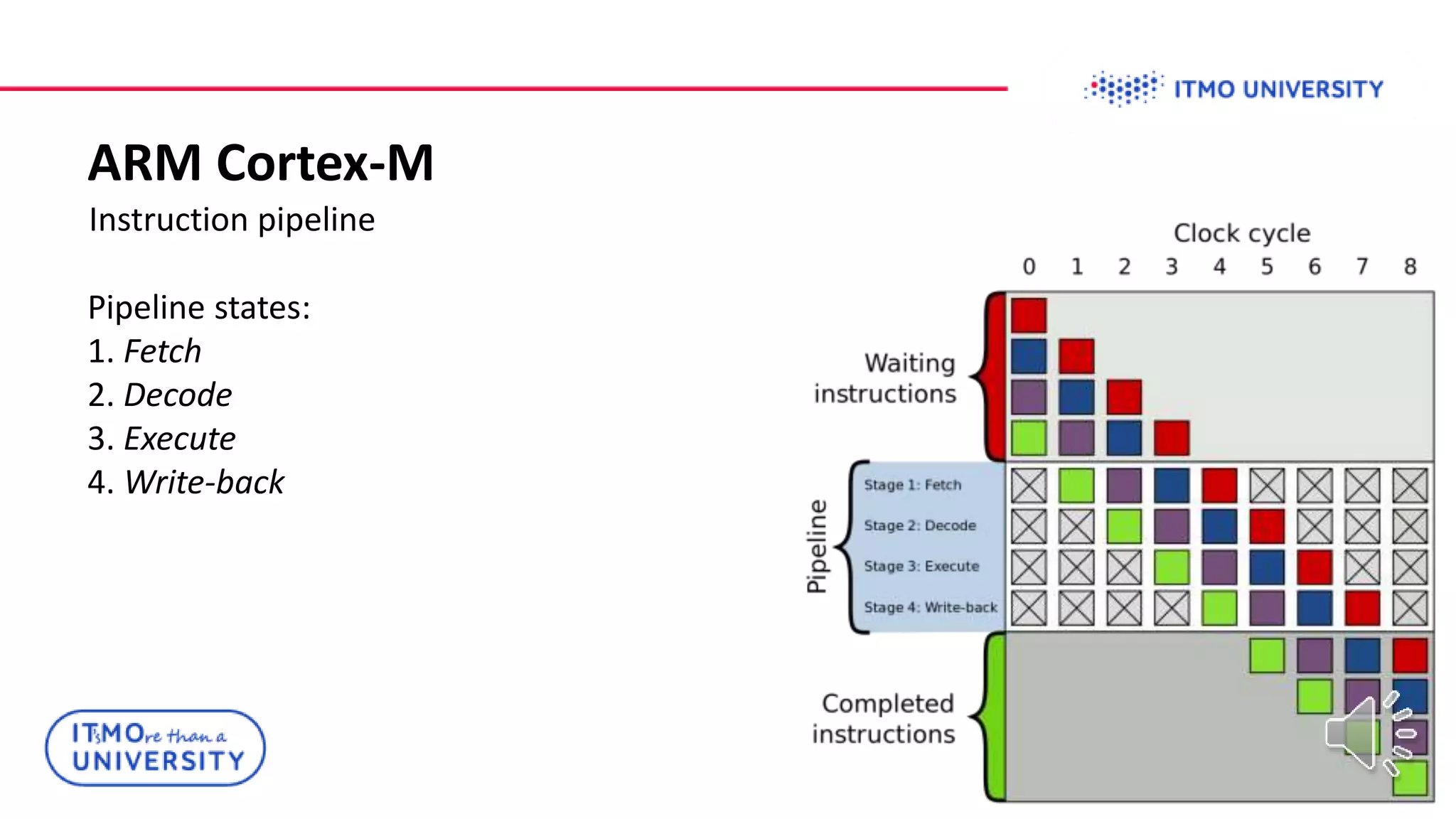
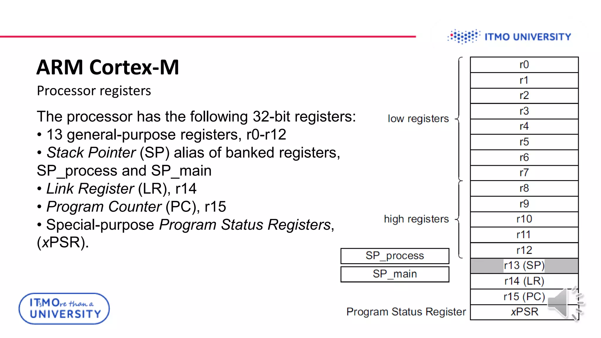
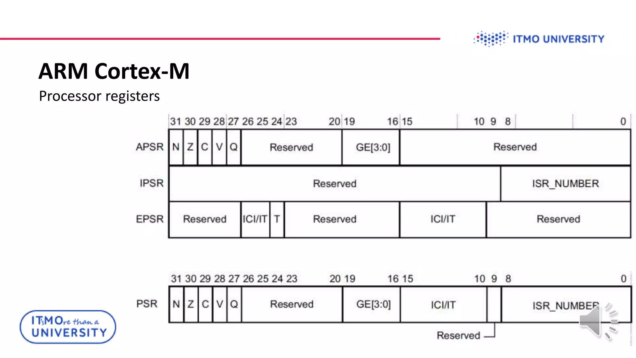
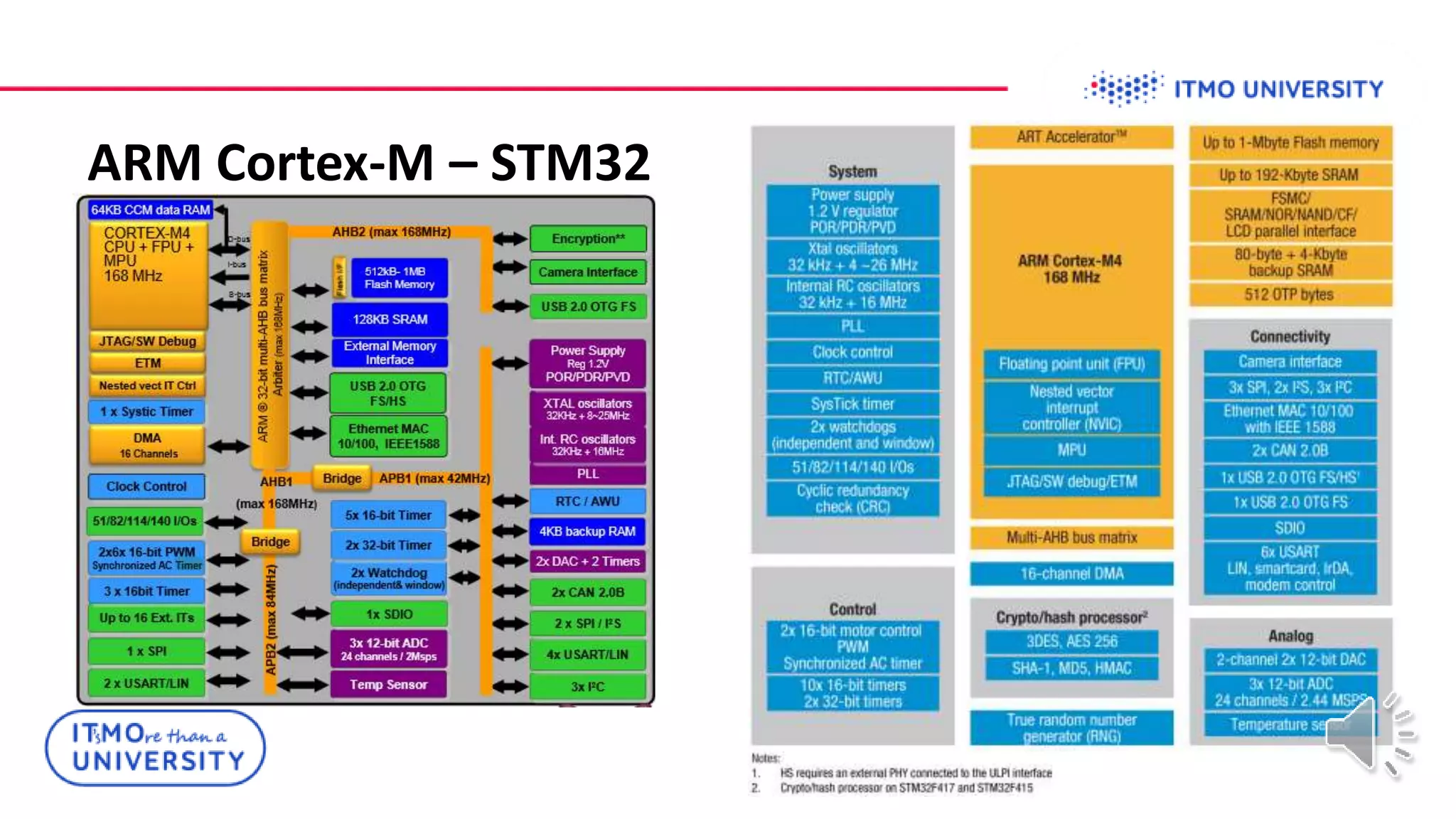
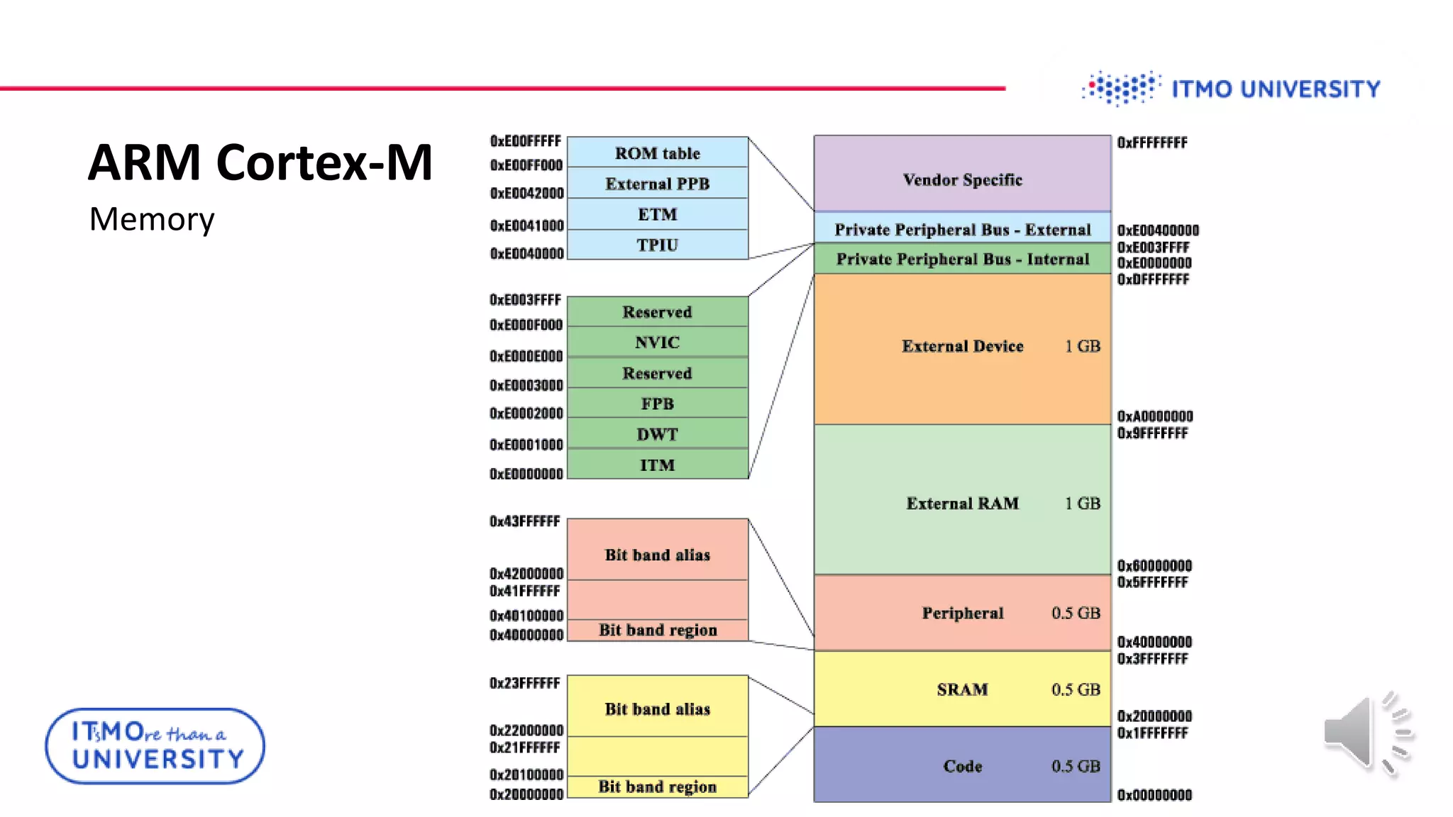
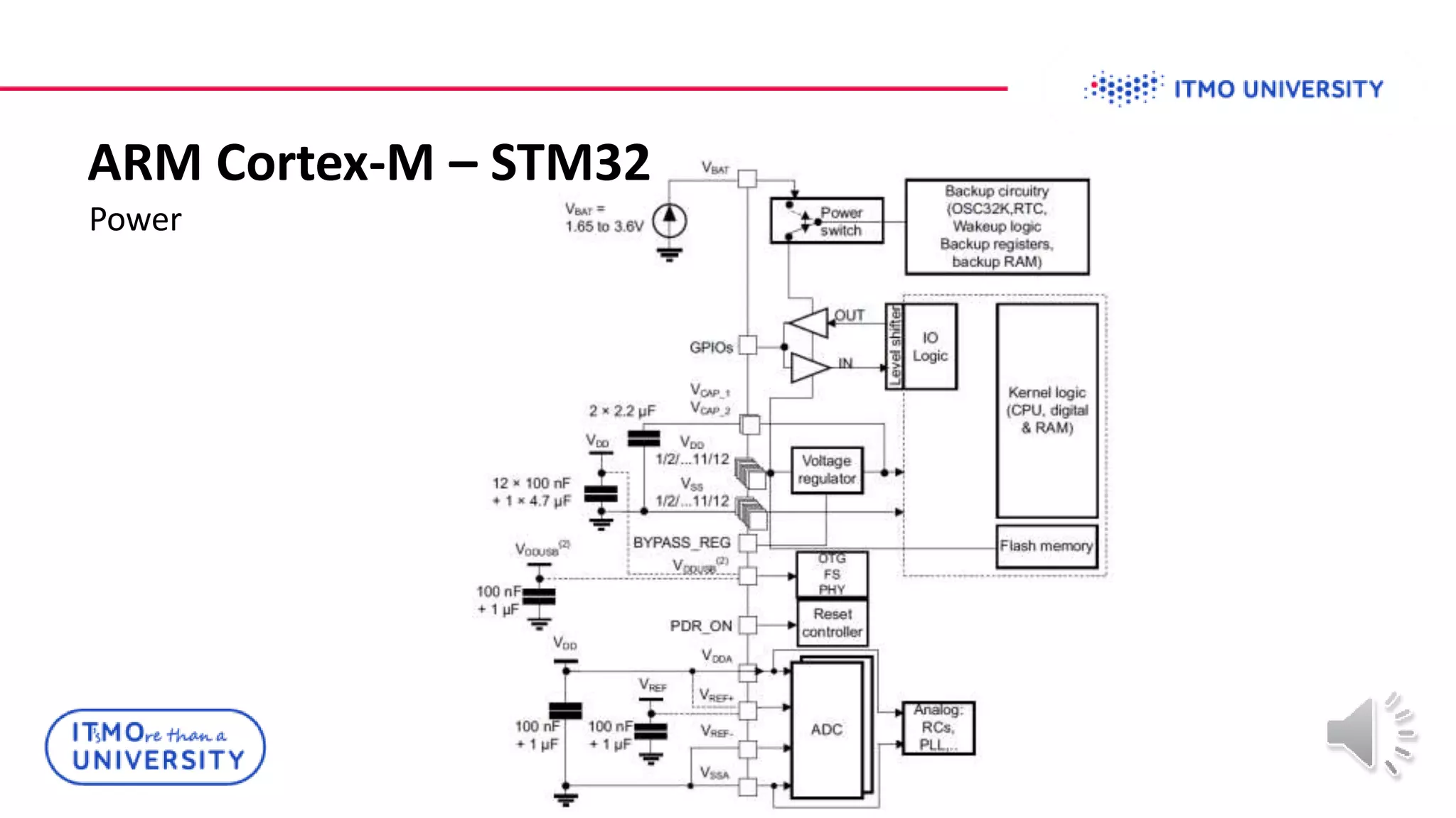
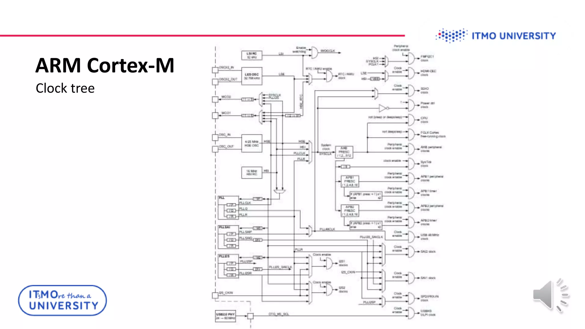
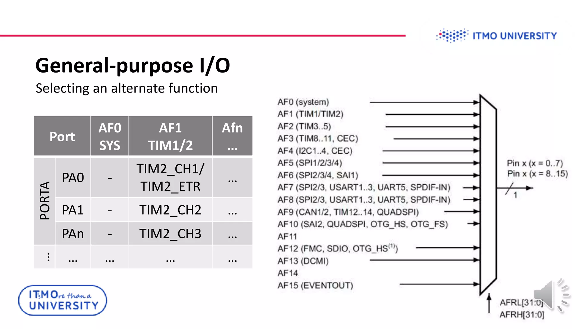
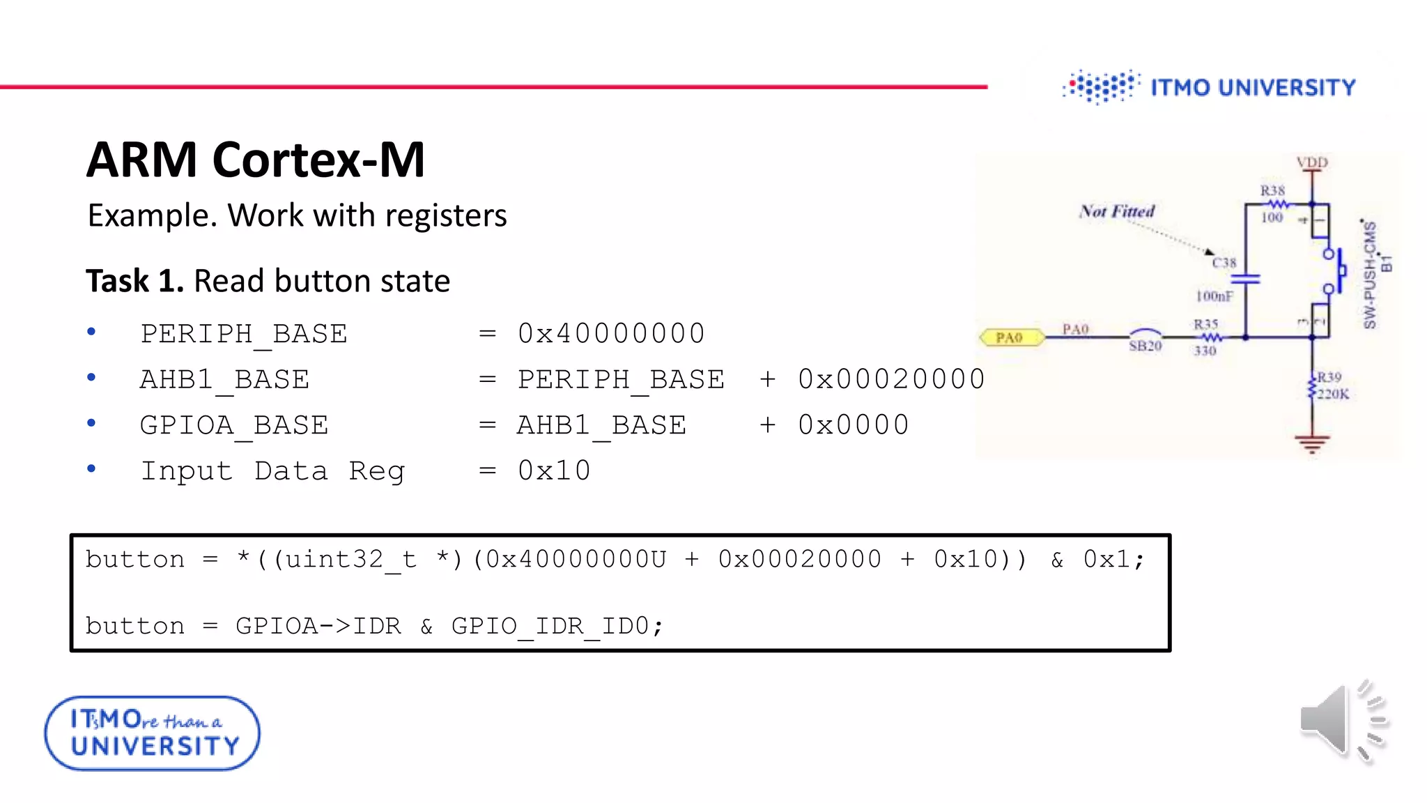
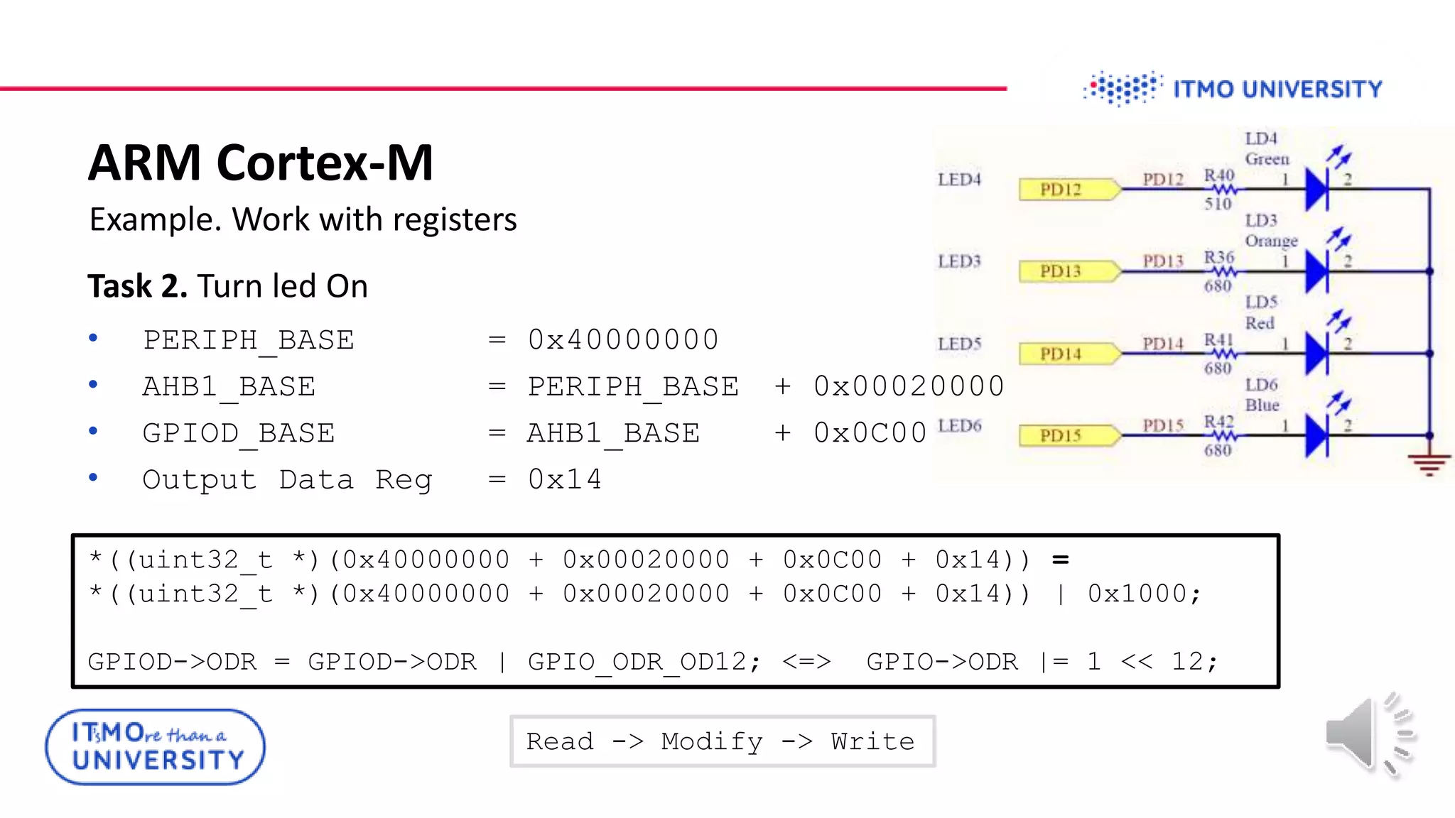
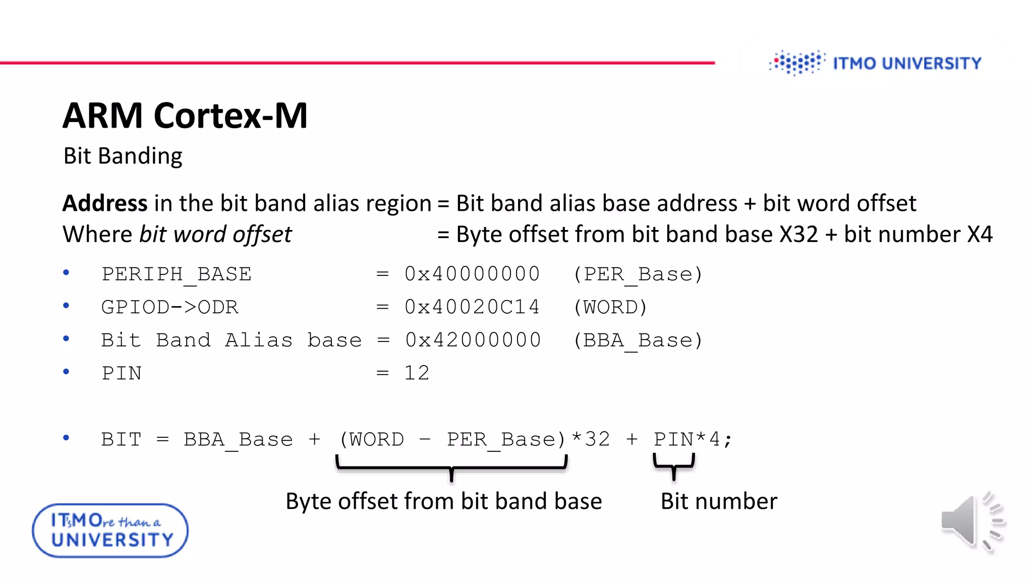
Microprocessors systems
Vlasov Sergey
smvlasov@itmo.ru
Kirsanova Aleksandra
ARM
Advanced RISC Machine <=> Acorn RISC Machine
• ARM7
• ARM9, ARM11
• Cortex A
• Cortex M
• Cortex-M0, Cortex-M0+, Cortex-M1
• Cortex-M3
• Cortex-M4, Cortex-M7
• Cortex-M23, Cortex-M33
RISC
reduced instruction set computer
• RISC processors use a small and limited number of
instructions
• RISC machines mostly uses hardwired control unit
• RISC processors consume less power and have high
performance
• Each instruction is very simple and consistent
• RISC processors use simple addressing modes
• RISC instruction is of uniform fixed length
• Large Number of Registers
ARM Cortex-M
• Microcontrollers
• ASIC (Application-specific integrated circuit)
• ASSP (Application-specific standard product)
• FPGA
• SoC (System-on-crystal)
ARM Cortex-M
Arm Core
Cortex
M0
Cortex
M0+
Cortex
M1
Cortex
M3
Cortex
M4
Cortex
M7
Cortex
M23
Cortex
M33
Cortex
M35P
ARM architecture ARMv6-M ARMv6-M ARMv6-M ARMv7-M ARMv7E-M ARMv7E-M
ARMv8-M
Baseline
ARMv8-M
Mainline
ARMv8-M
Mainline
Computer architecture
Von
Neuman
Von
Neumann
Von
Neumann
Harvard Harvard Harvard Von Neumann Harvard Harvard
Instruction pipeline 3 stages 2 stages 3 stages 3 stages 3 stages 6 stages 2 stages 3 stages 3 stages
Thumb-1 instructions Most Most Most Entire Entire Entire Most Entire Entire
Thumb-2 instructions Some Some Some Entire Entire Entire Some Entire Entire
Multiply instructions
32x32 = 32-bit result
Yes Yes Yes Yes Yes Yes Yes Yes Yes
Multiply instructions
32x32 = 64-bit result
No No No Yes Yes Yes No Yes Yes
Divide instructions
32/32 = 32-bit quotient
No No No Yes Yes Yes Yes Yes Yes
Saturated instructions No No No Some Yes Yes No Yes Yes
DSP instructions No No No No Yes Yes No Optional Optional
Interrupt latency
(if zero-wait state RAM)
16 cycles 15 cycles
23 for NMI
26 for IRQ
12 cycles 12 cycles 12 cycles
15 no security
ext
27 security ext
TBD TBD
ARM Cortex-M
Von Neumann (Princeton) Harvard
ARM Cortex-M
Instruction pipeline
•IF — Instruction Fetch,
•ID — Instruction Decode,
•EX — Execute,
•MEM — Memory access,
•WB — Register write back.
ARM Cortex-M
Instruction pipeline
Pipeline states:
1. Fetch
2. Decode
3. Execute
4. Write-back
ARM Cortex-M
Instruction pipeline
Pipeline states:
1. Fetch
2. Decode
3. Execute
4. Write-back
ARM Cortex-M
Processor registers
The processor has the following 32-bit registers:
• 13 general-purpose registers, r0-r12
• Stack Pointer (SP) alias of banked registers,
SP_process and SP_main
• Link Register (LR), r14
• Program Counter (PC), r15
• Special-purpose Program Status Registers,
(xPSR).
ARM Cortex-M
Processor registers
ARM Cortex-M
STM32
ARM Cortex-M – STM32
ARM Cortex-M
Memory
ARM Cortex-M – STM32
Power
ARM Cortex-M
Clock tree
General-purpose I/O
Main features
• Up to 16 I/Os under control
• Output states: push-pull or open drain + pull-up/down
• Output data from output data register (GPIOx_ODR)
• Speed selection for each I/O
• Input states: floating, pull-up/down, analog
• Input data to input data register (GPIOx_IDR)
• Bit set and reset register (GPIOx_BSRR) for bitwise write access to GPIOx_ODR
• Locking mechanism (GPIOx_LCKR) provided to freeze the I/O configuration
• Analog function
• Alternate function input/output selection registers (at most 16 AFs per I/O)
• Fast toggle capable of changing every two clock cycles
• Highly flexible pin multiplexing allows the use of I/O pins as GPIOs or as
one of several peripheral functions
General-purpose I/O
General-purpose I/O
Input configuration
General-purpose I/O
Output configuration
General-purpose I/O
Alternate function configuration
General-purpose I/O
Selecting an alternate function
Port
AF0
SYS
AF1
TIM1/2
Afn
…
PORTA
PA0 -
TIM2_CH1/
TIM2_ETR
…
PA1 - TIM2_CH2 …
PAn - TIM2_CH3 …
…
… … … …
General-purpose I/O
Analog configuration
ARM Cortex-M
Example. Work with registers
button = *((uint32_t *)(0x40000000U + 0x00020000 + 0x10)) & 0x1;
button = GPIOA->IDR & GPIO_IDR_ID0;
Task 1. Read button state
• PERIPH_BASE = 0x40000000
• AHB1_BASE = PERIPH_BASE + 0x00020000
• GPIOA_BASE = AHB1_BASE + 0x0000
• Input Data Reg = 0x10
ARM Cortex-M
Example. Work with registers
*((uint32_t *)(0x40000000 + 0x00020000 + 0x0C00 + 0x14)) =
*((uint32_t *)(0x40000000 + 0x00020000 + 0x0C00 + 0x14)) | 0x1000;
GPIOD->ODR = GPIOD->ODR | GPIO_ODR_OD12; <=> GPIO->ODR |= 1 << 12;
Task 2. Turn led On
• PERIPH_BASE = 0x40000000
• AHB1_BASE = PERIPH_BASE + 0x00020000
• GPIOD_BASE = AHB1_BASE + 0x0C00
• Output Data Reg = 0x14
Read -> Modify -> Write
ARM Cortex-M
Bit Banding
Address in the bit band alias region = Bit band alias base address + bit word offset
Where bit word offset = Byte offset from bit band base X32 + bit number X4
• PERIPH_BASE = 0x40000000 (PER_Base)
• GPIOD->ODR = 0x40020C14 (WORD)
• Bit Band Alias base = 0x42000000 (BBA_Base)
• PIN = 12
• BIT = BBA_Base + (WORD – PER_Base)*32 + PIN*4;
Byte offset from bit band base Bit number
Thank you for your attention
www.ifmo.ru

Lecture 1.pptx

  • 1.
  • 2.
    ARM Advanced RISC Machine<=> Acorn RISC Machine • ARM7 • ARM9, ARM11 • Cortex A • Cortex M • Cortex-M0, Cortex-M0+, Cortex-M1 • Cortex-M3 • Cortex-M4, Cortex-M7 • Cortex-M23, Cortex-M33
  • 3.
    RISC reduced instruction setcomputer • RISC processors use a small and limited number of instructions • RISC machines mostly uses hardwired control unit • RISC processors consume less power and have high performance • Each instruction is very simple and consistent • RISC processors use simple addressing modes • RISC instruction is of uniform fixed length • Large Number of Registers
  • 4.
    ARM Cortex-M • Microcontrollers •ASIC (Application-specific integrated circuit) • ASSP (Application-specific standard product) • FPGA • SoC (System-on-crystal)
  • 5.
    ARM Cortex-M Arm Core Cortex M0 Cortex M0+ Cortex M1 Cortex M3 Cortex M4 Cortex M7 Cortex M23 Cortex M33 Cortex M35P ARMarchitecture ARMv6-M ARMv6-M ARMv6-M ARMv7-M ARMv7E-M ARMv7E-M ARMv8-M Baseline ARMv8-M Mainline ARMv8-M Mainline Computer architecture Von Neuman Von Neumann Von Neumann Harvard Harvard Harvard Von Neumann Harvard Harvard Instruction pipeline 3 stages 2 stages 3 stages 3 stages 3 stages 6 stages 2 stages 3 stages 3 stages Thumb-1 instructions Most Most Most Entire Entire Entire Most Entire Entire Thumb-2 instructions Some Some Some Entire Entire Entire Some Entire Entire Multiply instructions 32x32 = 32-bit result Yes Yes Yes Yes Yes Yes Yes Yes Yes Multiply instructions 32x32 = 64-bit result No No No Yes Yes Yes No Yes Yes Divide instructions 32/32 = 32-bit quotient No No No Yes Yes Yes Yes Yes Yes Saturated instructions No No No Some Yes Yes No Yes Yes DSP instructions No No No No Yes Yes No Optional Optional Interrupt latency (if zero-wait state RAM) 16 cycles 15 cycles 23 for NMI 26 for IRQ 12 cycles 12 cycles 12 cycles 15 no security ext 27 security ext TBD TBD
  • 6.
    ARM Cortex-M Von Neumann(Princeton) Harvard
  • 7.
    ARM Cortex-M Instruction pipeline •IF— Instruction Fetch, •ID — Instruction Decode, •EX — Execute, •MEM — Memory access, •WB — Register write back.
  • 8.
    ARM Cortex-M Instruction pipeline Pipelinestates: 1. Fetch 2. Decode 3. Execute 4. Write-back
  • 9.
    ARM Cortex-M Instruction pipeline Pipelinestates: 1. Fetch 2. Decode 3. Execute 4. Write-back
  • 10.
    ARM Cortex-M Processor registers Theprocessor has the following 32-bit registers: • 13 general-purpose registers, r0-r12 • Stack Pointer (SP) alias of banked registers, SP_process and SP_main • Link Register (LR), r14 • Program Counter (PC), r15 • Special-purpose Program Status Registers, (xPSR).
  • 11.
  • 12.
  • 13.
  • 14.
  • 15.
  • 16.
    ARM Cortex-M –STM32 Power
  • 17.
  • 18.
    General-purpose I/O Main features •Up to 16 I/Os under control • Output states: push-pull or open drain + pull-up/down • Output data from output data register (GPIOx_ODR) • Speed selection for each I/O • Input states: floating, pull-up/down, analog • Input data to input data register (GPIOx_IDR) • Bit set and reset register (GPIOx_BSRR) for bitwise write access to GPIOx_ODR • Locking mechanism (GPIOx_LCKR) provided to freeze the I/O configuration • Analog function • Alternate function input/output selection registers (at most 16 AFs per I/O) • Fast toggle capable of changing every two clock cycles • Highly flexible pin multiplexing allows the use of I/O pins as GPIOs or as one of several peripheral functions
  • 19.
  • 20.
  • 21.
  • 22.
  • 23.
    General-purpose I/O Selecting analternate function Port AF0 SYS AF1 TIM1/2 Afn … PORTA PA0 - TIM2_CH1/ TIM2_ETR … PA1 - TIM2_CH2 … PAn - TIM2_CH3 … … … … … …
  • 24.
  • 25.
    ARM Cortex-M Example. Workwith registers button = *((uint32_t *)(0x40000000U + 0x00020000 + 0x10)) & 0x1; button = GPIOA->IDR & GPIO_IDR_ID0; Task 1. Read button state • PERIPH_BASE = 0x40000000 • AHB1_BASE = PERIPH_BASE + 0x00020000 • GPIOA_BASE = AHB1_BASE + 0x0000 • Input Data Reg = 0x10
  • 26.
    ARM Cortex-M Example. Workwith registers *((uint32_t *)(0x40000000 + 0x00020000 + 0x0C00 + 0x14)) = *((uint32_t *)(0x40000000 + 0x00020000 + 0x0C00 + 0x14)) | 0x1000; GPIOD->ODR = GPIOD->ODR | GPIO_ODR_OD12; <=> GPIO->ODR |= 1 << 12; Task 2. Turn led On • PERIPH_BASE = 0x40000000 • AHB1_BASE = PERIPH_BASE + 0x00020000 • GPIOD_BASE = AHB1_BASE + 0x0C00 • Output Data Reg = 0x14 Read -> Modify -> Write
  • 27.
    ARM Cortex-M Bit Banding Addressin the bit band alias region = Bit band alias base address + bit word offset Where bit word offset = Byte offset from bit band base X32 + bit number X4 • PERIPH_BASE = 0x40000000 (PER_Base) • GPIOD->ODR = 0x40020C14 (WORD) • Bit Band Alias base = 0x42000000 (BBA_Base) • PIN = 12 • BIT = BBA_Base + (WORD – PER_Base)*32 + PIN*4; Byte offset from bit band base Bit number
  • 28.
    Thank you foryour attention www.ifmo.ru