Lcd display
•Download as DOCX, PDF•
0 likes•263 views
here you can find the LCD DISPLAY pin description, characteristics, usage, and schematic diagram, source code. it is completely about 16x2 characteristic LCD.
Report
Share
Report
Share

Recommended
8051 Microcontroller I/O ports
Port 0 of the 8051 microcontroller can be used as a bidirectional I/O port or for address/data interfacing with external memory. When used as an input port, writing a 1 to the latch causes the output MOSFETs to turn off, allowing the pin value to be read directly. When used as an output port, a pull-up resistor is needed to write a 1 since the upper MOSFET turns off. Port 1 has internal pull-up resistors so no external resistors are needed, but the external device must sink current when writing a 0. Port 2 is similar to Port 1 for I/O but can also be used for higher address bytes. Port 3 pins each have alternate functions in
8051 Microcontroller PPT's By Er. Swapnil Kaware
The document describes the 8051 microcontroller, its features which include 4 I/O ports, 2 timers, serial communication interface, and interrupts. It discusses the internal architecture such as memory organization, registers, and oscillator circuit. The document also provides details on the ports, timers, serial communication, and power modes of the 8051 microcontroller.
Programmable peripheral interface 8255
8255 is a programmable I/O device that acts as an interface between peripheral devices and the microprocessor for parallel data transfer.
8255 presentaion.ppt
The 8255 Programmable Peripheral Interface chip is used to interface I/O devices with microprocessors. It has 3 ports - Port A, Port B, and Port C. Port C has two independent 4-bit ports. The 8255 can operate in I/O mode or Bit Set/Reset mode. In I/O mode, the ports can be configured for basic, strobed, or bidirectional I/O. The mode and port configurations are set using control words written to the chip.
An introduction to microprocessor architecture using INTEL 8085 as a classic...
The document provides an overview of the Intel 8085 microprocessor architecture. It describes that the 8085 is an 8-bit processor that can address 64KB of memory using 40 pins running at up to 3MHz. It discusses the address bus, data bus, control signals, and I/O pins. It also explains the CPU block diagram and details the functions of address latch enable, read, write, and I/O/memory selection signals. Machine cycles like opcode fetch, memory read and write are summarized. Interrupt handling and direct memory access are also covered at a high level.
I/O port programming in 8051
The document discusses the I/O ports of the 8051 microcontroller. It describes the four 8-bit I/O ports P0, P1, P2, and P3 and how each port can be configured as an input or output. It also discusses how individual bits within each port can be accessed and monitored using instructions like JNB and JB. The document explains the differences between reading the actual pin status versus reading the internal port latch, and how instructions like ANL P1,A utilize a read-modify-write feature to modify and write port values in a single step.
Isi and nyquist criterion
This document discusses techniques for pulse shaping to reduce inter-symbol interference (ISI) in digital communication systems. It introduces the Nyquist criteria that pulse shapes must satisfy to avoid ISI, including having zero crossings at symbol intervals, zero areas within symbol periods, and zero values at decision thresholds. Methods like raised cosine filtering are presented that trade off bandwidth for smoothness to meet the Nyquist criteria. The document also discusses partial response signaling techniques like duobinary that relax the criteria but require differential encoding to avoid error propagation.
Multipliers in VLSI
This document discusses various designs for digital multipliers. It begins by reviewing the basic building blocks used in digital circuits and how binary multiplication works by adding partial products. It then describes approaches for implementing multiplication, including right shift and add serial multipliers and faster parallel array and tree multipliers. Booth encoding is introduced as a technique to reduce the number of stages in a multiplier. Implementation details are provided for array and Wallace tree multipliers, including the use of compression cells like the (4,2) counter. Optimization goals for multipliers differ from adders in emphasizing reducing the critical path.
slide_logic_family_pune_SE_comp
This document provides an overview of digital logic families and integrated circuits (ICs). It discusses common logic families like TTL and CMOS, comparing their characteristics such as speed, power consumption, and noise immunity. It also describes common IC packages and the numbering systems used to identify standardized small-scale and medium-scale integrated circuits. Furthermore, it defines important electrical characteristics of logic families like voltage and current levels as well as timing parameters.
Low Power VLSI Design
Low Power VLSI design architecture for EDA (Electronic Design Automation) and Modern Power Estimation, Reduction and Fixing technologies including clock gating and power gating
Memory organization of 8051
The 8051 microcontroller has 128 bytes of internal RAM and 4Kbytes of internal ROM memory. It uses the same addresses for code and data but accesses the correct memory based on whether an operation is for code or data. The 128 bytes of internal RAM are organized into 4 banks of 32 bytes each. External memory can be added if more memory is needed for program code or variable data storage. The document also provides information on interfacing external program and data memory with the 8051 microcontroller.
MICROCONTROLLER 8051- Architecture & Pin Configuration
Architecture & Pin Configuration of MC8051 is very helpful to discuss the points and its easy to remember.
8051 microcontroller
This document provides an overview of the 8051 microcontroller architecture. It describes the basic components of the 8051 including 4K bytes of internal ROM, 128 bytes of internal RAM, four 8-bit I/O ports, two timers/counters, one serial interface, and other features. It also discusses the different addressing modes for 8051 assembly language programming including immediate, register, direct, register indirect, and external direct addressing.
Packaging of vlsi devices
This document discusses package design considerations and types of semiconductor packages. It covers key factors in package design like the number of terminals, electrical, thermal, and reliability requirements. The main package types discussed are through-hole packages like DIP and QFP, and surface mount packages like SOP, PLCC, and LCCC. Through-hole packages use precision holes drilled through the board while surface mount packages solder directly to the board surface.
CMOS Topic 5 -_cmos_inverter
This document discusses the CMOS inverter. It explains the switch models of the CMOS inverter and how the input signals determine whether the NMOS or PMOS transistor is on. It also discusses the properties of static CMOS inverters, including their voltage transfer characteristic curve and noise margins. The document describes how process variations and supply voltage scaling can impact the inverter's performance. Finally, it examines the dynamic behavior of the CMOS inverter and the parasitic capacitances that affect its switching speeds.
8086
The 8086 microprocessor is a 16-bit CPU launched by Intel in 1978. It has a 16-bit data bus and 20-bit address bus, allowing it to access up to 1MB of memory. The 8086 architecture partitions the CPU logic into two functional units - the Bus Interface Unit which handles external transactions, and the Execution Unit which performs decoding and execution. This separation improves processing speed by allowing parallel instruction fetching and execution via pipelining. The 8086 uses memory segmentation to access more memory than its 16-bit registers allow, dividing the 1MB address space into 64KB segments addressed using segment and offset registers.
CMOS Logic Circuits
This document discusses CMOS logic circuits. It begins by defining logic values and how bits are encoded using voltage levels. It then discusses different logic gates like inverters, NAND, NOR and buffers. It explains that logic gates are made from MOS transistors and describes the characteristics of N-type and P-type MOSFETs. The rest of the document discusses various electrical characteristics of CMOS logic circuits like logic levels, noise margins, input/output currents, fan-in, fan-out, propagation delay and power consumption. It also briefly mentions different CMOS logic families and issues around interfacing CMOS and TTL logic standards.
Interfacing Stepper motor with 8051
The document discusses interfacing a stepper motor with an 8051 microcontroller. A stepper motor can divide a full rotation into discrete steps through energizing coils in different sequences. The stepper motor can be interfaced with an 8051 using an L293D motor driver connected to ports P1.0, P1.2, P1.3, and P1.4 of the 8051. Both full-step and half-step sequences are described for energizing the coils to precisely control the motor's position without feedback. Assembly and C code examples are provided to demonstrate clockwise and counterclockwise rotation of the stepper motor connected to the 8051.
8086 modes
The document discusses the minimum and maximum mode systems of the 8086 microprocessor. In minimum mode, the 8086 generates all control signals and a single processor is used. In maximum mode, an external bus controller chip generates control signals and multiple processors can be used. It describes the components, address latching, read and write cycles, and I/O interfacing for both minimum and maximum mode 8086 systems.
Hardware View of Intel 8051
This presentation discusses the hardware details of 8051 microcontroller, viz. the pin description, reset circuit, port architectures, oscillator circuit and machine cycle etc in 8051
Layout & Stick Diagram Design Rules
This Presentation slides consists of the various design rules associated with layout & stick Diagrams with basic CMOS Gates explained.
Short Channel Effect In MOSFET
Know the versatile knowledge about MOSFET, it is the analysis at small level as short channeling in MOSFET
8051 interfacing
This consists of Interfacing of 8051 with ADC, DAC, LED, Seven segment Dispaly, Stepper motor, Temperature Sensor etc
Microcontroller 8051
The document discusses the Microcontroller 8051. It provides a block diagram and pin description of the 8051. It describes the registers, memory mapping, stack, I/O ports, timers and interrupts of the 8051 microcontroller. It compares microprocessors and microcontrollers, discussing the differences in hardware structure and applications.
CMOS
The document discusses CMOS technology which uses both NMOS and PMOS transistors in a complementary way. It has low power dissipation as power is only consumed during switching. CMOS circuits like inverters, NAND and NOR gates are constructed using a pull-up network of PMOS transistors and a pull-down network of NMOS transistors. The fabrication of CMOS transistors involves depositing and patterning materials on a silicon wafer through lithography. CMOS has advantages like low power, high noise immunity and is widely used in applications like computers, processors and memory chips.
Smart traffic light controller using verilog
This project will provides a detailed explanation about a smart traffic light controller using verilog code along with test bench and the working principle and simulation outputs are been attached.
Serial Communication in 8051
This presentation discusses the Serial Communication features in 8051, the support for UART. It also discusses serial vs parallel communication, simplex, duplex and full-duplex modes, MAX232, RS232 standards
8051 MICROCONTROLLER
The document discusses the 8051 microcontroller. It lists advantages of microcontroller-based systems such as lower cost, smaller size, and higher reliability compared to microprocessor-based systems. It describes some 8051 family members and compares their features such as ROM type, RAM size, and number of timers. It also discusses important components of the 8051 like ROM, RAM, I/O ports, timers, and serial port. The document provides block diagrams of the 8051 internal architecture and pinout. It describes the functions of various pins and registers.
Lcd interfacing
This document discusses interfacing a 16x2 LCD display module to an 8051 microcontroller. It provides the pin connections between the LCD and microcontroller, describes the LCD commands used to control the display, and includes two code examples in C language to initialize and write text to the LCD.
LCD Interacing with 8051
This presentation is all about interfacing of a character LCD with 8051 micro-controller. It discusses various LCD commands, LCD pin description and a simple LCD working code in assembly for interfacing.
More Related Content
What's hot
slide_logic_family_pune_SE_comp
This document provides an overview of digital logic families and integrated circuits (ICs). It discusses common logic families like TTL and CMOS, comparing their characteristics such as speed, power consumption, and noise immunity. It also describes common IC packages and the numbering systems used to identify standardized small-scale and medium-scale integrated circuits. Furthermore, it defines important electrical characteristics of logic families like voltage and current levels as well as timing parameters.
Low Power VLSI Design
Low Power VLSI design architecture for EDA (Electronic Design Automation) and Modern Power Estimation, Reduction and Fixing technologies including clock gating and power gating
Memory organization of 8051
The 8051 microcontroller has 128 bytes of internal RAM and 4Kbytes of internal ROM memory. It uses the same addresses for code and data but accesses the correct memory based on whether an operation is for code or data. The 128 bytes of internal RAM are organized into 4 banks of 32 bytes each. External memory can be added if more memory is needed for program code or variable data storage. The document also provides information on interfacing external program and data memory with the 8051 microcontroller.
MICROCONTROLLER 8051- Architecture & Pin Configuration
Architecture & Pin Configuration of MC8051 is very helpful to discuss the points and its easy to remember.
8051 microcontroller
This document provides an overview of the 8051 microcontroller architecture. It describes the basic components of the 8051 including 4K bytes of internal ROM, 128 bytes of internal RAM, four 8-bit I/O ports, two timers/counters, one serial interface, and other features. It also discusses the different addressing modes for 8051 assembly language programming including immediate, register, direct, register indirect, and external direct addressing.
Packaging of vlsi devices
This document discusses package design considerations and types of semiconductor packages. It covers key factors in package design like the number of terminals, electrical, thermal, and reliability requirements. The main package types discussed are through-hole packages like DIP and QFP, and surface mount packages like SOP, PLCC, and LCCC. Through-hole packages use precision holes drilled through the board while surface mount packages solder directly to the board surface.
CMOS Topic 5 -_cmos_inverter
This document discusses the CMOS inverter. It explains the switch models of the CMOS inverter and how the input signals determine whether the NMOS or PMOS transistor is on. It also discusses the properties of static CMOS inverters, including their voltage transfer characteristic curve and noise margins. The document describes how process variations and supply voltage scaling can impact the inverter's performance. Finally, it examines the dynamic behavior of the CMOS inverter and the parasitic capacitances that affect its switching speeds.
8086
The 8086 microprocessor is a 16-bit CPU launched by Intel in 1978. It has a 16-bit data bus and 20-bit address bus, allowing it to access up to 1MB of memory. The 8086 architecture partitions the CPU logic into two functional units - the Bus Interface Unit which handles external transactions, and the Execution Unit which performs decoding and execution. This separation improves processing speed by allowing parallel instruction fetching and execution via pipelining. The 8086 uses memory segmentation to access more memory than its 16-bit registers allow, dividing the 1MB address space into 64KB segments addressed using segment and offset registers.
CMOS Logic Circuits
This document discusses CMOS logic circuits. It begins by defining logic values and how bits are encoded using voltage levels. It then discusses different logic gates like inverters, NAND, NOR and buffers. It explains that logic gates are made from MOS transistors and describes the characteristics of N-type and P-type MOSFETs. The rest of the document discusses various electrical characteristics of CMOS logic circuits like logic levels, noise margins, input/output currents, fan-in, fan-out, propagation delay and power consumption. It also briefly mentions different CMOS logic families and issues around interfacing CMOS and TTL logic standards.
Interfacing Stepper motor with 8051
The document discusses interfacing a stepper motor with an 8051 microcontroller. A stepper motor can divide a full rotation into discrete steps through energizing coils in different sequences. The stepper motor can be interfaced with an 8051 using an L293D motor driver connected to ports P1.0, P1.2, P1.3, and P1.4 of the 8051. Both full-step and half-step sequences are described for energizing the coils to precisely control the motor's position without feedback. Assembly and C code examples are provided to demonstrate clockwise and counterclockwise rotation of the stepper motor connected to the 8051.
8086 modes
The document discusses the minimum and maximum mode systems of the 8086 microprocessor. In minimum mode, the 8086 generates all control signals and a single processor is used. In maximum mode, an external bus controller chip generates control signals and multiple processors can be used. It describes the components, address latching, read and write cycles, and I/O interfacing for both minimum and maximum mode 8086 systems.
Hardware View of Intel 8051
This presentation discusses the hardware details of 8051 microcontroller, viz. the pin description, reset circuit, port architectures, oscillator circuit and machine cycle etc in 8051
Layout & Stick Diagram Design Rules
This Presentation slides consists of the various design rules associated with layout & stick Diagrams with basic CMOS Gates explained.
Short Channel Effect In MOSFET
Know the versatile knowledge about MOSFET, it is the analysis at small level as short channeling in MOSFET
8051 interfacing
This consists of Interfacing of 8051 with ADC, DAC, LED, Seven segment Dispaly, Stepper motor, Temperature Sensor etc
Microcontroller 8051
The document discusses the Microcontroller 8051. It provides a block diagram and pin description of the 8051. It describes the registers, memory mapping, stack, I/O ports, timers and interrupts of the 8051 microcontroller. It compares microprocessors and microcontrollers, discussing the differences in hardware structure and applications.
CMOS
The document discusses CMOS technology which uses both NMOS and PMOS transistors in a complementary way. It has low power dissipation as power is only consumed during switching. CMOS circuits like inverters, NAND and NOR gates are constructed using a pull-up network of PMOS transistors and a pull-down network of NMOS transistors. The fabrication of CMOS transistors involves depositing and patterning materials on a silicon wafer through lithography. CMOS has advantages like low power, high noise immunity and is widely used in applications like computers, processors and memory chips.
Smart traffic light controller using verilog
This project will provides a detailed explanation about a smart traffic light controller using verilog code along with test bench and the working principle and simulation outputs are been attached.
Serial Communication in 8051
This presentation discusses the Serial Communication features in 8051, the support for UART. It also discusses serial vs parallel communication, simplex, duplex and full-duplex modes, MAX232, RS232 standards
8051 MICROCONTROLLER
The document discusses the 8051 microcontroller. It lists advantages of microcontroller-based systems such as lower cost, smaller size, and higher reliability compared to microprocessor-based systems. It describes some 8051 family members and compares their features such as ROM type, RAM size, and number of timers. It also discusses important components of the 8051 like ROM, RAM, I/O ports, timers, and serial port. The document provides block diagrams of the 8051 internal architecture and pinout. It describes the functions of various pins and registers.
What's hot (20)
MICROCONTROLLER 8051- Architecture & Pin Configuration
MICROCONTROLLER 8051- Architecture & Pin Configuration
Similar to Lcd display
Lcd interfacing
This document discusses interfacing a 16x2 LCD display module to an 8051 microcontroller. It provides the pin connections between the LCD and microcontroller, describes the LCD commands used to control the display, and includes two code examples in C language to initialize and write text to the LCD.
LCD Interacing with 8051
This presentation is all about interfacing of a character LCD with 8051 micro-controller. It discusses various LCD commands, LCD pin description and a simple LCD working code in assembly for interfacing.
Arduino based applications part 2
1) LCDs can display characters, images, or fixed displays and use pixels to show information. Different types include character LCDs for text, graphic LCDs for images, and graphic LCDs with touch panels for input.
2) Character LCDs have small rectangles to display characters or small icons while graphic LCDs have a big grid of pixels for images. Graphic LCDs are larger, more expensive, and complex.
3) A speaker can make beeps, tones, and alerts for uses like alarms, timers, and user input feedback. It connects to an Arduino and can be coded to play tones at different frequencies.
Hd44780a00 dtasheet
This document provides information about interfacing with an HD44780 24x2 LCD display. It describes the display's specifications including its controller chips, pinout, character set, and protocol for sending data and commands. Custom characters can be defined by sending bitmap data. The display is supported directly by the Serial Wombat microcontroller which can control the LCD along with other devices through a simple RS-232 connection.
LCD (2).pptx
LCD stands for liquid crystal display. It can display alphanumeric characters and is commonly available in 16x2, 16x4, 32x2, and 32x4 sizes, but all LCDs have the same 16 GPIO pins for interfacing. The LCD has 10 programmable pins including RS, EN, and data pins D0-D7, and 6 hardware pins including ground, VCC, and contrast. It can operate in 8-bit or 4-bit mode and needs to receive command and text data.
Basic of Firmware & Embedded Software Programming in C
Basic of Firmware & Embedded Software Programming in C
Interfacing with LCD
This document describes experiments with interfacing a microcontroller to a character LCD. It is divided into three parts: 1) Displaying a single letter on the LCD, 2) Displaying a string of characters, and 3) Shifting a message left and right continuously. The author explains the LCD module features and registers. Algorithms and flowcharts are provided for writing bytes to the LCD by first checking the busy flag and then sending command or data. Displaying a single letter "A" is achieved by writing the character data to the specified LCD coordinate.
Microcontroller part 4
Here are the key steps for how SPI works:
1. The master device initiates the data transfer by selecting a slave device using the chip select (CS) line. This brings the slave device online.
2. The master outputs the clock signal (SCLK) which is used by both the master and slave devices to synchronize the data transfer.
3. The master sends data on the MOSI (master out, slave in) line which the slave receives on its SDI pin in sync with the clock.
4. In parallel, the slave sends data on the MISO (master in, slave out) line which the master receives on its SDO pin, also in sync with the clock.
Lecture mp 7(interface)
This document outlines the course content for a microcontroller design course. It covers topics like 8051 and PIC18F microcontroller architecture, assembly language programming, timers, interrupts, and design examples. It provides details on interfacing memory, LCD displays, and servo motors to microcontrollers. Examples of address decoding, writing to RAM and initializing an LCD are described. The document acknowledges the course material is used with permission from the head of the Mechatronics Engineering department at NUST.
LCD WITH 8051.docx
This document describes how to interface an LCD display with an 8051 microcontroller kit. It provides details on the LCD module including its pinout, commands, initialization process, and sending data. It also includes the circuit diagram showing how the LCD is connected to the microcontroller ports and includes components for backlight control and contrast adjustment. The aim is to understand the interface between an LCD display and the 8051 microcontroller.
8051.pdf
Here are the steps to interface external RAM to 8051 microcontroller:
1. Connect the RD pin of 8051 to the OE (Output Enable) pin of the external RAM. This will enable the RAM during read operations.
2. Connect the WR pin of 8051 to the WE (Write Enable) pin of the external RAM. This will enable writing into the RAM during write operations.
3. Connect the active low input of a NAND gate to the CE (Chip Enable) pin of the external RAM.
4. Connect the other input of the NAND gate to EA pin of 8051.
5. Connect the output of the NAND gate to the PSEN (Program Store Enable
2. 8085-Microprocessor.pptx
The 8085 microprocessor is an 8-bit CPU with 40 pins that requires a +5V power supply. It has an 8-bit data bus and 16-bit address bus that can access up to 64KB of memory. The 8085 architecture includes six 8-bit registers (BC, DE, HL), an 8-bit accumulator, 16-bit program counter, 16-bit stack pointer, and 5-bit flag register. The multiplexed address/data bus is used to transfer both addresses and data. Control signals include RD, WR, ALE and status signals S1 and S0 are used to indicate read, write and other operations to memory or I/O devices.
Automatic room light controller with visible counter
This project creates an automatic room light controller that also counts visitors bidirectionally. When someone enters the room, the counter increments and the light turns on. When someone leaves, the counter decrements and the light turns off once the room is empty. A password must be entered using a keypad to unlock the room. The system uses an ATmega16 microcontroller, infrared sensors, an LCD display, relays and other components. It provides functions like automatic lighting control, visitor counting and secured access with a password. The design aims to ease complexity and control room congestion.
8085 micro processor
The document provides information about the Intel 8085 microprocessor. Some key details include:
- It is an 8-bit processor that operates on a 5V power supply with a maximum clock frequency of 3MHz.
- It has 40 pins and uses a multiplexed address/data bus. It can access 64KB of memory space and 256 I/O ports.
- It has one accumulator, flag, and six general purpose registers. It supports various addressing modes and 74 instructions.
- Interrupts include TRAP, RST 5.5, RST 6.5, RST 7.5, and INTR. Serial I/O is also supported directly.
-
Introduction to embedded system & density based traffic light system
The document discusses embedded systems and embedded development. It begins with examples of embedded systems in daily life. It then covers embedded system block diagrams and various embedded processors like microprocessors, microcontrollers, DSP processors, and ASICs. It also discusses common microcontroller and microprocessor families like 8051, PIC, AVR, ARM, Intel and AMD. Finally, it presents some example embedded projects and how to interface components like LEDs, switches, seven segment displays to microcontrollers.
08_lcd.pdf
- Liquid crystal displays (LCDs) contain small dots that can be controlled to display images or text. Some LCDs contain a controller chip like the HD44780 to simplify displaying alphanumeric text.
- The HD44780 controller chip allows data to be sent in 8-bit or 4-bit mode through control lines like RS, R/W, EN, and data lines DB0-DB7.
- The mikroC library provides functions to initialize and write text or commands to an LCD using the 4-bit mode with functions like Lcd_Init(), Lcd_Out(), and Lcd_Cmd().
MCS51 Training board
Model CATC2016A
This document provides instructions and a bill of materials for building a training board for the MCS51 microcontroller. It includes:
1. A schematic diagram and overview of the reset circuit, crystal oscillator, LED display, input switches, and external connections.
2. A parts list with 20 components needed including an MCS51 CPU, LEDs, buttons, headers, and a 7-segment display.
3. Guidelines for drilling holes in the PCB board and notes on materials needed like the PCB, etching solution, and drill bits.
4. A small coding project example to count up from 0-9 on the 7-segment display while walking a single LED across the row.
Calculator design with lcd using fpga
This document describes the design and implementation of a basic calculator using an LCD display module with an FPGA. It includes objectives to write Verilog code for the calculator logic and driving the LCD display. The design is a simple four-function calculator that takes two single-digit inputs and an operation and displays the result. The document outlines the state machine design and functions for converting values to ASCII format for the LCD. It provides details on interfacing with and controlling the LCD module through its control lines and registers. The implementation in Verilog is described including the top module ports and behavioral simulation steps to test the design functionality.
ARM LCD Interfacing
This document discusses interfacing a 16x2 LCD with an ARM processor. It begins with an introduction to 16x2 LCDs, describing their pinout, display data RAM (DDRAM), character generator ROM (CGROM), character generator RAM (CGRAM), and control flags. It then covers initializing the LCD in both 4-bit and 8-bit modes through sending a sequence of commands. The document demonstrates initializing and sending data to the LCD. It concludes with briefly mentioning interfacing the LCD with ARM and providing an assignment to display and scroll text on the LCD.
Similar to Lcd display (20)
Basic of Firmware & Embedded Software Programming in C
Basic of Firmware & Embedded Software Programming in C
Automatic room light controller with visible counter
Automatic room light controller with visible counter
Introduction to embedded system & density based traffic light system
Introduction to embedded system & density based traffic light system
Recently uploaded
VARIABLE FREQUENCY DRIVE. VFDs are widely used in industrial applications for...
Variable frequency drive .A Variable Frequency Drive (VFD) is an electronic device used to control the speed and torque of an electric motor by varying the frequency and voltage of its power supply. VFDs are widely used in industrial applications for motor control, providing significant energy savings and precise motor operation.
2008 BUILDING CONSTRUCTION Illustrated - Ching Chapter 08 Doors and Windows.pdf
2008 BUILDING CONSTRUCTION Illustrated - Ching Chapter 08 Doors and Windows
Prediction of Electrical Energy Efficiency Using Information on Consumer's Ac...
Energy efficiency has been important since the latter part of the last century. The main object of this survey is to determine the energy efficiency knowledge among consumers. Two separate districts in Bangladesh are selected to conduct the survey on households and showrooms about the energy and seller also. The survey uses the data to find some regression equations from which it is easy to predict energy efficiency knowledge. The data is analyzed and calculated based on five important criteria. The initial target was to find some factors that help predict a person's energy efficiency knowledge. From the survey, it is found that the energy efficiency awareness among the people of our country is very low. Relationships between household energy use behaviors are estimated using a unique dataset of about 40 households and 20 showrooms in Bangladesh's Chapainawabganj and Bagerhat districts. Knowledge of energy consumption and energy efficiency technology options is found to be associated with household use of energy conservation practices. Household characteristics also influence household energy use behavior. Younger household cohorts are more likely to adopt energy-efficient technologies and energy conservation practices and place primary importance on energy saving for environmental reasons. Education also influences attitudes toward energy conservation in Bangladesh. Low-education households indicate they primarily save electricity for the environment while high-education households indicate they are motivated by environmental concerns.
LLM Fine Tuning with QLoRA Cassandra Lunch 4, presented by Anant
Slides for the 4th Presentation on LLM Fine-Tuning with QLoRA Presented by Anant, featuring DataStax Astra
一比一原版(爱大毕业证书)爱荷华大学毕业证如何办理
原版一模一样【微信:741003700 】【(爱大毕业证书)爱荷华大学毕业证成绩单】【微信:741003700 】学位证,留信认证(真实可查,永久存档)原件一模一样纸张工艺/offer、雅思、外壳等材料/诚信可靠,可直接看成品样本,帮您解决无法毕业带来的各种难题!外壳,原版制作,诚信可靠,可直接看成品样本。行业标杆!精益求精,诚心合作,真诚制作!多年品质 ,按需精细制作,24小时接单,全套进口原装设备。十五年致力于帮助留学生解决难题,包您满意。
本公司拥有海外各大学样板无数,能完美还原。
1:1完美还原海外各大学毕业材料上的工艺:水印,阴影底纹,钢印LOGO烫金烫银,LOGO烫金烫银复合重叠。文字图案浮雕、激光镭射、紫外荧光、温感、复印防伪等防伪工艺。材料咨询办理、认证咨询办理请加学历顾问Q/微741003700
【主营项目】
一.毕业证【q微741003700】成绩单、使馆认证、教育部认证、雅思托福成绩单、学生卡等!
二.真实使馆公证(即留学回国人员证明,不成功不收费)
三.真实教育部学历学位认证(教育部存档!教育部留服网站永久可查)
四.办理各国各大学文凭(一对一专业服务,可全程监控跟踪进度)
如果您处于以下几种情况:
◇在校期间,因各种原因未能顺利毕业……拿不到官方毕业证【q/微741003700】
◇面对父母的压力,希望尽快拿到;
◇不清楚认证流程以及材料该如何准备;
◇回国时间很长,忘记办理;
◇回国马上就要找工作,办给用人单位看;
◇企事业单位必须要求办理的
◇需要报考公务员、购买免税车、落转户口
◇申请留学生创业基金
留信网认证的作用:
1:该专业认证可证明留学生真实身份
2:同时对留学生所学专业登记给予评定
3:国家专业人才认证中心颁发入库证书
4:这个认证书并且可以归档倒地方
5:凡事获得留信网入网的信息将会逐步更新到个人身份内,将在公安局网内查询个人身份证信息后,同步读取人才网入库信息
6:个人职称评审加20分
7:个人信誉贷款加10分
8:在国家人才网主办的国家网络招聘大会中纳入资料,供国家高端企业选择人才
办理(爱大毕业证书)爱荷华大学毕业证【微信:741003700 】外观非常简单,由纸质材料制成,上面印有校徽、校名、毕业生姓名、专业等信息。
办理(爱大毕业证书)爱荷华大学毕业证【微信:741003700 】格式相对统一,各专业都有相应的模板。通常包括以下部分:
校徽:象征着学校的荣誉和传承。
校名:学校英文全称
授予学位:本部分将注明获得的具体学位名称。
毕业生姓名:这是最重要的信息之一,标志着该证书是由特定人员获得的。
颁发日期:这是毕业正式生效的时间,也代表着毕业生学业的结束。
其他信息:根据不同的专业和学位,可能会有一些特定的信息或章节。
办理(爱大毕业证书)爱荷华大学毕业证【微信:741003700 】价值很高,需要妥善保管。一般来说,应放置在安全、干燥、防潮的地方,避免长时间暴露在阳光下。如需使用,最好使用复印件而不是原件,以免丢失。
综上所述,办理(爱大毕业证书)爱荷华大学毕业证【微信:741003700 】是证明身份和学历的高价值文件。外观简单庄重,格式统一,包括重要的个人信息和发布日期。对持有人来说,妥善保管是非常重要的。
Applications of artificial Intelligence in Mechanical Engineering.pdf
Historically, mechanical engineering has relied heavily on human expertise and empirical methods to solve complex problems. With the introduction of computer-aided design (CAD) and finite element analysis (FEA), the field took its first steps towards digitization. These tools allowed engineers to simulate and analyze mechanical systems with greater accuracy and efficiency. However, the sheer volume of data generated by modern engineering systems and the increasing complexity of these systems have necessitated more advanced analytical tools, paving the way for AI.
AI offers the capability to process vast amounts of data, identify patterns, and make predictions with a level of speed and accuracy unattainable by traditional methods. This has profound implications for mechanical engineering, enabling more efficient design processes, predictive maintenance strategies, and optimized manufacturing operations. AI-driven tools can learn from historical data, adapt to new information, and continuously improve their performance, making them invaluable in tackling the multifaceted challenges of modern mechanical engineering.
一比一原版(CalArts毕业证)加利福尼亚艺术学院毕业证如何办理
CalArts毕业证学历书【微信95270640】CalArts毕业证’圣力嘉学院毕业证《Q微信95270640》办理CalArts毕业证√文凭学历制作{CalArts文凭}购买学历学位证书本科硕士,CalArts毕业证学历学位证【实体公司】办毕业证、成绩单、学历认证、学位证、文凭认证、办留信网认证、(网上可查,实体公司,专业可靠)
(诚招代理)办理国外高校毕业证成绩单文凭学位证,真实使馆公证(留学回国人员证明)真实留信网认证国外学历学位认证雅思代考国外学校代申请名校保录开请假条改GPA改成绩ID卡
1.高仿业务:【本科硕士】毕业证,成绩单(GPA修改),学历认证(教育部认证),大学Offer,,ID,留信认证,使馆认证,雅思,语言证书等高仿类证书;
2.认证服务: 学历认证(教育部认证),大使馆认证(回国人员证明),留信认证(可查有编号证书),大学保录取,雅思保分成绩单。
3.技术服务:钢印水印烫金激光防伪凹凸版设计印刷激凸温感光标底纹镭射速度快。
办理加利福尼亚艺术学院加利福尼亚艺术学院毕业证文凭证书流程:
1客户提供办理信息:姓名生日专业学位毕业时间等(如信息不确定可以咨询顾问:我们有专业老师帮你查询);
2开始安排制作毕业证成绩单电子图;
3毕业证成绩单电子版做好以后发送给您确认;
4毕业证成绩单电子版您确认信息无误之后安排制作成品;
5成品做好拍照或者视频给您确认;
6快递给客户(国内顺丰国外DHLUPS等快读邮寄)
-办理真实使馆公证(即留学回国人员证明)
-办理各国各大学文凭(世界名校一对一专业服务,可全程监控跟踪进度)
-全套服务:毕业证成绩单真实使馆公证真实教育部认证。让您回国发展信心十足!
(详情请加一下 文凭顾问+微信:95270640)欢迎咨询!子小伍玩小伍比山娃小一岁虎头虎脑的很霸气父亲让山娃跟小伍去夏令营听课山娃很高兴夏令营就设在附近一所小学山娃发现那所小学比自己的学校更大更美操场上还铺有塑胶跑道呢里面很多小朋友一班一班的快快乐乐原来城里娃都藏这儿来了怪不得平时见不到他们山娃恍然大悟起来吹拉弹唱琴棋书画山娃都不懂却什么都想学山娃怨自己太笨什么都不会斟酌再三山娃终于选定了学美术当听说每月要交元时父亲犹豫了山娃也说爸算了吧咱学校一学期才转
Redefining brain tumor segmentation: a cutting-edge convolutional neural netw...
Medical image analysis has witnessed significant advancements with deep learning techniques. In the domain of brain tumor segmentation, the ability to
precisely delineate tumor boundaries from magnetic resonance imaging (MRI)
scans holds profound implications for diagnosis. This study presents an ensemble convolutional neural network (CNN) with transfer learning, integrating
the state-of-the-art Deeplabv3+ architecture with the ResNet18 backbone. The
model is rigorously trained and evaluated, exhibiting remarkable performance
metrics, including an impressive global accuracy of 99.286%, a high-class accuracy of 82.191%, a mean intersection over union (IoU) of 79.900%, a weighted
IoU of 98.620%, and a Boundary F1 (BF) score of 83.303%. Notably, a detailed comparative analysis with existing methods showcases the superiority of
our proposed model. These findings underscore the model’s competence in precise brain tumor localization, underscoring its potential to revolutionize medical
image analysis and enhance healthcare outcomes. This research paves the way
for future exploration and optimization of advanced CNN models in medical
imaging, emphasizing addressing false positives and resource efficiency.
Electric vehicle and photovoltaic advanced roles in enhancing the financial p...
Climate change's impact on the planet forced the United Nations and governments to promote green energies and electric transportation. The deployments of photovoltaic (PV) and electric vehicle (EV) systems gained stronger momentum due to their numerous advantages over fossil fuel types. The advantages go beyond sustainability to reach financial support and stability. The work in this paper introduces the hybrid system between PV and EV to support industrial and commercial plants. This paper covers the theoretical framework of the proposed hybrid system including the required equation to complete the cost analysis when PV and EV are present. In addition, the proposed design diagram which sets the priorities and requirements of the system is presented. The proposed approach allows setup to advance their power stability, especially during power outages. The presented information supports researchers and plant owners to complete the necessary analysis while promoting the deployment of clean energy. The result of a case study that represents a dairy milk farmer supports the theoretical works and highlights its advanced benefits to existing plants. The short return on investment of the proposed approach supports the paper's novelty approach for the sustainable electrical system. In addition, the proposed system allows for an isolated power setup without the need for a transmission line which enhances the safety of the electrical network
Optimizing Gradle Builds - Gradle DPE Tour Berlin 2024
Sinan from the Delivery Hero mobile infrastructure engineering team shares a deep dive into performance acceleration with Gradle build cache optimizations. Sinan shares their journey into solving complex build-cache problems that affect Gradle builds. By understanding the challenges and solutions found in our journey, we aim to demonstrate the possibilities for faster builds. The case study reveals how overlapping outputs and cache misconfigurations led to significant increases in build times, especially as the project scaled up with numerous modules using Paparazzi tests. The journey from diagnosing to defeating cache issues offers invaluable lessons on maintaining cache integrity without sacrificing functionality.
一比一原版(osu毕业证书)美国俄勒冈州立大学毕业证如何办理
原版一模一样【微信:741003700 】【(osu毕业证书)美国俄勒冈州立大学毕业证成绩单】【微信:741003700 】学位证,留信认证(真实可查,永久存档)原件一模一样纸张工艺/offer、雅思、外壳等材料/诚信可靠,可直接看成品样本,帮您解决无法毕业带来的各种难题!外壳,原版制作,诚信可靠,可直接看成品样本。行业标杆!精益求精,诚心合作,真诚制作!多年品质 ,按需精细制作,24小时接单,全套进口原装设备。十五年致力于帮助留学生解决难题,包您满意。
本公司拥有海外各大学样板无数,能完美还原。
1:1完美还原海外各大学毕业材料上的工艺:水印,阴影底纹,钢印LOGO烫金烫银,LOGO烫金烫银复合重叠。文字图案浮雕、激光镭射、紫外荧光、温感、复印防伪等防伪工艺。材料咨询办理、认证咨询办理请加学历顾问Q/微741003700
【主营项目】
一.毕业证【q微741003700】成绩单、使馆认证、教育部认证、雅思托福成绩单、学生卡等!
二.真实使馆公证(即留学回国人员证明,不成功不收费)
三.真实教育部学历学位认证(教育部存档!教育部留服网站永久可查)
四.办理各国各大学文凭(一对一专业服务,可全程监控跟踪进度)
如果您处于以下几种情况:
◇在校期间,因各种原因未能顺利毕业……拿不到官方毕业证【q/微741003700】
◇面对父母的压力,希望尽快拿到;
◇不清楚认证流程以及材料该如何准备;
◇回国时间很长,忘记办理;
◇回国马上就要找工作,办给用人单位看;
◇企事业单位必须要求办理的
◇需要报考公务员、购买免税车、落转户口
◇申请留学生创业基金
留信网认证的作用:
1:该专业认证可证明留学生真实身份
2:同时对留学生所学专业登记给予评定
3:国家专业人才认证中心颁发入库证书
4:这个认证书并且可以归档倒地方
5:凡事获得留信网入网的信息将会逐步更新到个人身份内,将在公安局网内查询个人身份证信息后,同步读取人才网入库信息
6:个人职称评审加20分
7:个人信誉贷款加10分
8:在国家人才网主办的国家网络招聘大会中纳入资料,供国家高端企业选择人才
办理(osu毕业证书)美国俄勒冈州立大学毕业证【微信:741003700 】外观非常简单,由纸质材料制成,上面印有校徽、校名、毕业生姓名、专业等信息。
办理(osu毕业证书)美国俄勒冈州立大学毕业证【微信:741003700 】格式相对统一,各专业都有相应的模板。通常包括以下部分:
校徽:象征着学校的荣誉和传承。
校名:学校英文全称
授予学位:本部分将注明获得的具体学位名称。
毕业生姓名:这是最重要的信息之一,标志着该证书是由特定人员获得的。
颁发日期:这是毕业正式生效的时间,也代表着毕业生学业的结束。
其他信息:根据不同的专业和学位,可能会有一些特定的信息或章节。
办理(osu毕业证书)美国俄勒冈州立大学毕业证【微信:741003700 】价值很高,需要妥善保管。一般来说,应放置在安全、干燥、防潮的地方,避免长时间暴露在阳光下。如需使用,最好使用复印件而不是原件,以免丢失。
综上所述,办理(osu毕业证书)美国俄勒冈州立大学毕业证【微信:741003700 】是证明身份和学历的高价值文件。外观简单庄重,格式统一,包括重要的个人信息和发布日期。对持有人来说,妥善保管是非常重要的。
Object Oriented Analysis and Design - OOAD
This ppt gives detailed description of Object Oriented Analysis and design.
Generative AI Use cases applications solutions and implementation.pdf
Generative AI solutions encompass a range of capabilities from content creation to complex problem-solving across industries. Implementing generative AI involves identifying specific business needs, developing tailored AI models using techniques like GANs and VAEs, and integrating these models into existing workflows. Data quality and continuous model refinement are crucial for effective implementation. Businesses must also consider ethical implications and ensure transparency in AI decision-making. Generative AI's implementation aims to enhance efficiency, creativity, and innovation by leveraging autonomous generation and sophisticated learning algorithms to meet diverse business challenges.
https://www.leewayhertz.com/generative-ai-use-cases-and-applications/
Mechanical Engineering on AAI Summer Training Report-003.pdf
Mechanical Engineering PROJECT REPORT ON SUMMER VOCATIONAL TRAINING
AT MBB AIRPORT
Gas agency management system project report.pdf
The project entitled "Gas Agency" is done to make the manual process easier by making it a computerized system for billing and maintaining stock. The Gas Agencies get the order request through phone calls or by personal from their customers and deliver the gas cylinders to their address based on their demand and previous delivery date. This process is made computerized and the customer's name, address and stock details are stored in a database. Based on this the billing for a customer is made simple and easier, since a customer order for gas can be accepted only after completing a certain period from the previous delivery. This can be calculated and billed easily through this. There are two types of delivery like domestic purpose use delivery and commercial purpose use delivery. The bill rate and capacity differs for both. This can be easily maintained and charged accordingly.
Software Engineering and Project Management - Software Testing + Agile Method...
Software Testing: A Strategic Approach to Software Testing, Strategic Issues, Test Strategies for Conventional Software, Test Strategies for Object -Oriented Software, Validation Testing, System Testing, The Art of Debugging.
Agile Methodology: Before Agile – Waterfall, Agile Development.
Recently uploaded (20)
VARIABLE FREQUENCY DRIVE. VFDs are widely used in industrial applications for...
VARIABLE FREQUENCY DRIVE. VFDs are widely used in industrial applications for...
2008 BUILDING CONSTRUCTION Illustrated - Ching Chapter 08 Doors and Windows.pdf
2008 BUILDING CONSTRUCTION Illustrated - Ching Chapter 08 Doors and Windows.pdf
Prediction of Electrical Energy Efficiency Using Information on Consumer's Ac...
Prediction of Electrical Energy Efficiency Using Information on Consumer's Ac...
LLM Fine Tuning with QLoRA Cassandra Lunch 4, presented by Anant
LLM Fine Tuning with QLoRA Cassandra Lunch 4, presented by Anant
Applications of artificial Intelligence in Mechanical Engineering.pdf
Applications of artificial Intelligence in Mechanical Engineering.pdf
Redefining brain tumor segmentation: a cutting-edge convolutional neural netw...
Redefining brain tumor segmentation: a cutting-edge convolutional neural netw...
Electric vehicle and photovoltaic advanced roles in enhancing the financial p...
Electric vehicle and photovoltaic advanced roles in enhancing the financial p...
Optimizing Gradle Builds - Gradle DPE Tour Berlin 2024
Optimizing Gradle Builds - Gradle DPE Tour Berlin 2024
Generative AI Use cases applications solutions and implementation.pdf
Generative AI Use cases applications solutions and implementation.pdf
Mechanical Engineering on AAI Summer Training Report-003.pdf
Mechanical Engineering on AAI Summer Training Report-003.pdf
Software Engineering and Project Management - Software Testing + Agile Method...
Software Engineering and Project Management - Software Testing + Agile Method...
Lcd display
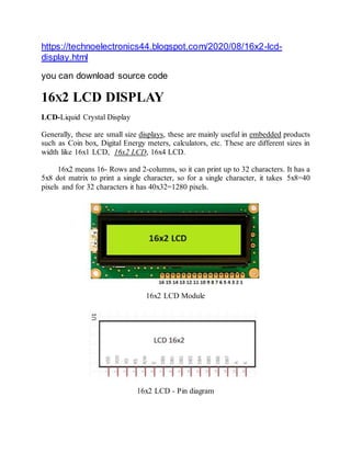
- 1. https://technoelectronics44.blogspot.com/2020/08/16x2-lcd- display.html you can download source code 16X2 LCD DISPLAY LCD-Liquid Crystal Display Generally, these are small size displays, these are mainly useful in embedded products such as Coin box, Digital Energy meters, calculators, etc. These are different sizes in width like 16x1 LCD, 16x2 LCD, 16x4 LCD. 16x2 means 16- Rows and 2-columns, so it can print up to 32 characters. It has a 5x8 dot matrix to print a single character, so for a single character, it takes 5x8=40 pixels and for 32 characters it has 40x32=1280 pixels. 16x2 LCD Module 16x2 LCD - Pin diagram
- 2. Features Operating Voltage: 4.5v-5.5v Output maximum current: 5ma Total pins: 16 Built-in controller (HD44780 or Equivalent) Back led color: Blue, Green, Yellow. Rows /column: 16x2 Total characters: 16 Alphanumeric LCD display It can operate in an 8-bit or 4-bit data mode. 5x8 dot matrix for character representation Pin configuration 1 Vss Ground 2 Vcc/Vdd 5v(Positive terminal) 3 VE Contrast (brightness adjustment) 4 RS Register Select (to select Data mode or command mode) 5 R/W Read / Write Operation 6 EN Enable 7 D0 Data pin 0 8 D1 Data pin 1 9 D2 Data pin 2 10 D3 Data pin 3 11 D4 Data pin 4 12 D5 Data pin 5 13 D6 Data pin 6 14 D7 Data pin 7 15 A Anode (Backlight positive terminal) 16 K Cathode (Backlight negative terminal) Power supply pins Vdd – is the power supply positive pin Vss – is the power supply negative pin A – Anode terminal (positive terminal of Back Light LED) K – Cathode terminal (Negative terminal of Back Light LED) Contrast pin
- 3. Vee – to adjust the Backlight LED brightness By adjusting the voltage across this pin brightness will be adjust. Control pins RS – Register select, it is useful to select the command mode or data mode of operation RS=0 for command mode, whereas RS=1 for data mode. R/W – To perform the Read and write operation (Write Operation is an active LOW signal) En –Enable pin, we can assign the instructions by triggering the Enable pin. Data pins D0-D8 = Usually it has 8-data pins. It supports two modes of operations. 8-bit data mode 4-bit data mode You can select any one of the modes by using the commands, and there is no effect on performance. Commands Sr. No Code Command description 1 0x01 Clear display screen 2 0x02 Return home 3 0x04 Decrement cursor (shift cursor to left) 4 0x06 Increment cursor (shift cursor to right)/Entry mode 5 0x05 Shift display right 6 0x07 Shift display left 7 0x08 Display off, cursor off 8 0x0A Display off, cursor on 9 0x0C Display on, cursor off 10 0x0E Display on, cursor on 11 0x0F Display on, cursor blinking 12 0x10 Shift cursor position to left by one character
- 4. 13 0x14 Shift cursor position to right by one character 14 0x18 Shift the entire display to the left 15 0x1C Shift the entire display to the right 16 0x80 Force cursor to the beginning ( 1st line) 17 0xC0 Force cursor to the beginning ( 2nd line) 18 0x38 2 lines and 5×7 matrix 19 0x28 1 Line and 5x7 matrix HOW TO USE LCD? HOW TO IMPLEMENT LCD PROGRAM? Applications Digital Energy meters Telephone Coin boxes. Gaming devices Calculators Alternative Displays 8x1 LCD, 8x2 LCD, 16x4 LCD, I2C 16x2 LCD Display Related Articles 16x2 LCD interface with Arduino