Call Girls Delhi {Jodhpur} 9711199012 high profile service
Iaetsd design and implementation of
1. DESIGN AND IMPLEMENTATION OF
ULTRASONIC TRANSDUCERS USING
HV CLASS-F POWER AMPLIFIER
Jeyasree Tagore1
, V.Vidhya2
,
M. E.Applied Electronics, M. E.Applied Electronics,
Sriram Engineering College, Sriram Engineering College,
Perumalpattu, Chennai, Perumalpattu, Chennai,
Tamilnadu, India Tamilnadu, India
jeyatag@gmail.com vidhyasreeeee@gmail.com.
ABSTRACT
This paper provides an integrated, high efficiency,
high voltage, class-F Power Amplifier (PA) for
increasing the efficiency of Ultrasonic Transducer. It
also provides harmonic termination technique for
high efficiency class F PA’s. The effect of different
output harmonic terminations on the Power- Added
Efficiency (PAE) of the PA has also been analyzed.
Theoretically, high efficiency can be attained in class-
F operation by maximally flattening the current and
voltage waveforms at the drain of active device.
Keywords: Ultrasound transmitter, Class-F PA, Power
Added Efficiency, Harmonic Termination Network.
I. INTRODUCTION
THE ULTRASOUND transmitter, which generates
high voltage (HV) signals to excite the transducers,
is one of the most critical components in the entire
medical ultrasound imaging system. Most of
today’s commercial medical ultrasound machines
use HV digital pulsers (unipolar or bipolar) as the
transmitters. These digital pulsers, in spites of
being simple, usually contain high harmonic
components with a second-order harmonic
distortion (HD2) between −30 and −40 dB. Real
time ultra-sound imaging systems have been
available for more than thirty years. Nonetheless,
considerable advancement in the function of ultra-
sound systems and output display is presently
underway. Integration and advanced electronics
play a key role in ultrasound imaging. The
advancement in deep sub-micron CMOS
technology is easily achievable for digital signal
and low-frequency signal processing. However, in
order to reach the final goal of System-on-a-Chip
(SoC) solution, the final piece of puzzle is still
missing – the RF front end. In fact, being the most
power hungry component of the RF front end is the
RF power amplifier (PA). It is one of the most
critical building blocks in low power SoC
integration.
II. BASIC BLOCK DIAGRAM
Different PA classes can be divided into two major
groups: linear and non-linear PAs. Class A, AB, B
and C PA are some of the well-known linear PAs,
which are distinguished primarily by their bias
condition. Linear PAs have the advantage of high
linearity that is important for variable envelope
modulation schemes (e.g. p/4-QPSK). However,
linear amplifiers suffer from poor maximum power
efficiency which limits their applications in low
power devices. In practice, an efficiency of only
below 20% can be achieved in those systems. In
contrast, non-linear PAs (also known as switched
mode PAs) can achieve better efficiency. As
suggested by its name, non-linear PAs have poor
linearity performance. Nevertheless, it is still
acceptable for constant envelope modulation
schemes (e.g. FSK). To overcome the problem of
linearity to adapt to variable envelope systems,
many linearization techniques have been proposed
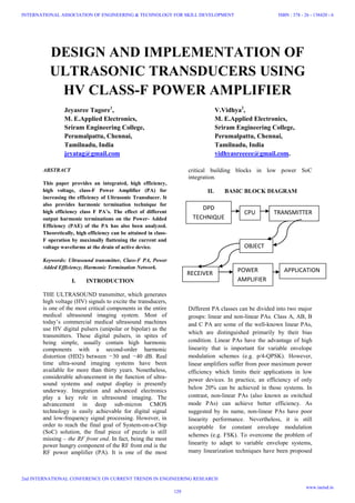
DPD
TECHNIQUE
CPU TRANSMITTER
APPLICATIONPOWER
AMPLIFIER
RECEIVER
OBJECT
129
INTERNATIONAL ASSOCIATION OF ENGINEERING & TECHNOLOGY FOR SKILL DEVELOPMENT
2nd INTERNATIONAL CONFERENCE ON CURRENT TRENDS IN ENGINEERING RESEARCH
ISBN : 378 - 26 - 138420 - 6
www.iaetsd.in
2. for non-linear amplifiers. Therefore, due their high
efficiency and the development of linearization
techniques, non-linear PAs have received more
attention over linear topologies in mobile
communication in the last decade. Class E and F
are the most common classes of non-linear PAs. In
comparison, Class E PA requires fast switching
driver signal that is not required for Class-F PA.
Moreover, because of relatively large switch
stresses to active devices, Class E amplifiers do not
scale gracefully with the trend toward lower-power
technology with lower breakdown voltage. For
these reasons, Class-F PA has drawn more
attention for its easier implementation and better
integration with sub-micron CMOS technology.
This project proposes a clear cut idea of increasing
the efficiency and resolution of ultrasound images
by the use of Class F RF Power Amplifier.
III. HARMONIC TERMINATION OF CLASS
F POWER AMPLIFIER
Several design methods have been proposed to
enable multi-band operation of various circuits
such as impedance transformers low-noise
amplifiers (LNAs), mixers, and PAs. The design of
multi-band PAs is challenging as stringent
requirements on the efficiency, output power, and
linearity have to be satisfied. In modern
transmitters, harmonic-tuned PAs (e.g., class-F) are
preferred to their linear counterparts to achieve
higher efficiencies. The harmonic termination
network (HTN) should provide open-circuit
impedance in the drain of the transistors at odd-
order harmonics and the short-circuit impedance at
the even-order harmonics for class-F operation.
Most of the proposed HTNs for class-F PAs are
limited to terminating up to three harmonics. Three
general approaches have been developed for multi-
band operation of PAs [9]. Several PA units can be
connected in parallel and optimized for each band,
while the band selection is performed using
switches or diplexers. Another approach is based
on using reconfigurable components, e.g.,
varactors, in the matching networks. The third
approach is based on employing multi-band
impedance matching networks. This approach
enables concurrent operation of the PA at multiple
frequency bands and also avoids the use of
switches or reconfigurable elements with control
voltages. Achieving multi-band operation for class-
F PAs is more challenging than linear PAs as the
HTN should provide proper impedance
terminations for fundamental frequencies as well as
their harmonics at several distinct frequency bands.
The HTNs reported for concurrent multi-band
class-F PAs are mostly limited to two frequency
bands and provide terminations for up to three
harmonic.
A method for terminating higher number of
harmonics is shown in Fig. 1(a). The drain and gate
bias lines are embedded in the HTNs. This obviates
the need for the RF choke that commonly is
realized using a large inductor or a quarter-
wavelength transmission line (TL). Thus, the bias
lines are reused by the HTNs and the chip area is
reduced. The HTNs ideally provide open-circuit
impedance at the frequency of operation, ωo, while
the matching networks transform the load/source
resistance into the optimum load/source impedance
of the transistor ( ZL,opt and ZS,opt ) that maximizes
the output power or efficiency. At the harmonics of
ωo, the matching networks exhibit open circuit,
while the HTNs are designed to provide open
circuit at the odd-order harmonics and short circuit
at the even-order harmonics. The open-circuit
condition of impedance matching networks at
harmonics of can be achieved by using multiple
parallel LC networks inserted in series with each
other, each resonating at one of the harmonics.
However, this method requires a large number of
elements that their loss, especially at the output
matching network, degrades efficiency of the PA.
Another method is to adopt a series LC network
resonating at ωo. This network exhibits short
circuit impedance at frequency of operation, while
at the nth
harmonic of ωo it provides reactive
impedance of (n-1/n) ωoL . The inductance should
be chosen large enough that this impedance can
approximately provide an open-circuit condition,
i.e., it should be much larger than other impedance
levels in the circuit. It should be noted that this
impedance increases with the order of harmonic,
indicating that it is enough to provide the open-
circuit condition at the second harmonic. This
series LC network can also be reused in the
matching network for impedance transformation. In
practice, the impedance matching network at
harmonics of introduces large impedance in
parallel with parasitic capacitance of the transistor
that should also be absorbed into the HTN. The
effects of this impedance can be accounted for
using circuit simulations. The equivalent circuit of
the HTN is shown in Fig. 1(b), where Cp denotes
the output/input parasitic capacitance of the
transistor. The network order is n+1 , where n is an
odd number. Depending on frequency of operation
and the transistor physical layout and packaging,
the parasitic inductances in series with the gate and
drain terminals can also have sensible effect on the
PA performance. The output/input series parasitic
inductance of the transistor can be accounted for by
Ln.
130
INTERNATIONAL ASSOCIATION OF ENGINEERING & TECHNOLOGY FOR SKILL DEVELOPMENT
2nd INTERNATIONAL CONFERENCE ON CURRENT TRENDS IN ENGINEERING RESEARCH
ISBN : 378 - 26 - 138420 - 6
www.iaetsd.in
3. Fig. 1. (a) Proposed harmonic termination
technique for class-F PAs
(b) Equivalent HTN.
IV. DIGITAL PREDISTORTION
TECHNIQUE
To reduce the harmonic distortions from the
transmitter, a DPD linearization technique is
designed and implemented. The DPD system is
composed of a digital-to-analog converter (DAC),
an analog-to-digital converter, and a field
programmable gate array (FPGA) where the digital
components for the DPD algorithm, the delay
synchronization unit, and the lookup table memory
are implemented. The DPD linearization is divided
into two stages: calibration and evaluation. At the
beginning of the calibration stage t0, the DPD
FPGA and the DAC send an ideal input sinusoidal
calibration signal u(t) to the input, where the output
of the amplifier o(t) can be expressed as a Taylor
expansion in terms of u(t), i.e., o(t) = A1 ・ u(t) +
A2 ・ u(t)2 + A3 ・ u(t)3 +… where A1, A2, and
A3 are the first-, second-, and third order gains of
the amplifier. As discussed in [15], the output
signal of the amplifier is attenuated, fed back into
the DPD FPGA, delay adjusted, and then
subtracted into the ideal input signal to equalize the
input containing the inverse response of the power
amplifier nonlinearities. During the evaluation
stage, the equalized amplifier output signal
becomes
oeq(t + tD) =A1 ・ eq(ωt)+A2 ・ eq(2ωt)+A3 ・
eq(3ωt)+… =A1 ・ u(ωt) + residue, where tD is the
amplifier group delay, eq(ωt) is the equalized input
signal with ω being the angular frequency, and
residue is the remaining harmonic components
above the fourth order.
V. IMPLEMENTATION AND
EXPERIMENTAL RESULTS
Fig. 2. Schematic representation of a Class AB that
is modified to a Class- F power amplifier.
The class-F amplifiers with the nonlinear capacitor
are investigated. To validate the voltage waveform
shaping by the nonlinear output capacitor and the
highly efficient operation of the saturated amplifier,
we designed and implemented the amplifier at
2.655 GHz using the Cree GaN HEMT CGH40010
packaged device containing a CGH60015 bare die.
Since the commercial device model includes the
package effects such as the bonding wires, package
leads, and parasitic, the simulation is carried out
using the bare-chip model to explore the inherent
operation of the saturated amplifier. In addition, the
saturated amplifier is compared with the class-F
amplifier using the bare-chip model. For the
implementation, the packaged device containing
the bare chip is employed for simulation and to
build the amplifier.
Fig.3 shows the simulated efficiencies and power
gains of the class-F and saturated amplifiers using
the bare-chip model. As expected, the saturated
amplifier delivers the improved gain and efficiency
characteristic compared to the class-F amplifier.
However, the gain compression is not that fast. The
efficiency curves for the two PAs are also similar
to the previous simulation result. Fig. 4 shows the
second harmonic load–pull contours and time-
domain voltage and current waveforms of the
saturated amplifier using the bare-chip model.
During the simulation, the fundamental and third
harmonic loads are set to and, respectively. Due to
the harmonic generation of the nonlinear output
capacitor, the high efficiency is maintained across
the wide second harmonic impedance region.
Moreover, even if the input power is low, the half
sinusoidal voltage waveform is generated, proving
the harmonic generation by the nonlinear output
capacitor.
131
INTERNATIONAL ASSOCIATION OF ENGINEERING & TECHNOLOGY FOR SKILL DEVELOPMENT
2nd INTERNATIONAL CONFERENCE ON CURRENT TRENDS IN ENGINEERING RESEARCH
ISBN : 378 - 26 - 138420 - 6
www.iaetsd.in
4. Fig.3. Simulated efficiencies and power gains of
the class-F and saturated amplifiers using a real
device.
Fig. 4. Simulated and measured output power,
drain efficiency, PAE and power gain.
VI. CONCLUSION
Table I. Comparison between Class AB and Class
F Power Amplifier.
Thus an integrated HV power amplifier for medical
ultrasound transmitters to be used in advanced
ultrasonic imaging modes such as THI for
enhanced imaging quality is designed. A current
feedback technique, a DPD technique, and a
dynamic biasing current modulation technique are
used to improve the power amplifier’s bandwidth,
output signal linearity, and power efficiency. The
HV power amplifier is fabricated using a 1-μm HV
process. Measurement results indicate that the
linear power amplifier is capable of driving a load
of a 100-Ω resistor in parallel with a 300-Pf
capacitor with a signal voltage swing up to 180 Vpp
and an HD2 as low as −50 dB. Measurement
results also show that the amplifier achieves a
maximum slew rate of 4 V/ns and a power
efficiency of 60%.
REFERENCE
1. An Integrated High-Voltage Low-Distortion Current-
Feedback Linear Power Amplifier for Ultrasound
Transmitters Using Digital Pre-distortion and
Dynamic Current Biasing Techniques Zheng Gao,
Ping Gui, Senior Member, IEEE, and Rick
Jordanger, IEEE Transactions on circuits and
systems—ii: Express briefs, vol. 61, no. 6, June
2014.
2. Analysis and Design of a High Voltage Integrated
Class-B Amplifier for Ultra-Sound Transducers,
IEEE Transaction on Circuits and system, July, 2014.
3. A Harmonic Termination Technique for Single- and
Multi-Band High-Efficiency Class-F MMIC Power
Amplifiers, IEEE TRANSACTIONS ON
MICROWAVE THEORY AND TECHNIQUES,
VOL. 62, NO. 5, MAY 2014.
4. Characterization of Class-F Power Amplifier With
Wide Amplitude and Phase Bandwidth for Out-
phasing Architecture, IEEE MICROWAVE AND
WIRELESS COMPONENTS LETTERS, VOL. 24,
NO. 3, MARCH 2014.
5. A Class F-1/F 24-to-31GHz Power Amplifier with
40.7% Peak PAE, 15dBm OP1dB, and 50mW Psat
in 0.13μm SiGe BiCMOS, 2014 IEEE International
Solid-State Circuits Conference, 978-1-4799-0920-
9/14/$31.00 c2014.
6. Digitally Modified Filter-less Receiver for 2D
Digital Pre-distortion Of Concurrent Dual-Band
Power Amplifiers, 978·1-4799-3869-8/14/$31.00
®2014.
7. Behaviors of class F and class F¯¹ Amplifiers, IEEE
Transactions on Microwave Theory and Techniques,
June 2012.
8. Design of a Class F Power Amplifiers,
PIERSONLINE, VOL.6, NO.2, 2010.
9. High efficiency Class F Power Amplifier Design, 0-
7803- 8246- 1/ 04/ $20.00 2004, IEEE.
Amplifier Pout
(dBm)
Gain (dB) Efficiency
(%)
Class AB 33.89 17.89 40.09
Class F 34.66 17.86 65.17(appro
x)
132
INTERNATIONAL ASSOCIATION OF ENGINEERING & TECHNOLOGY FOR SKILL DEVELOPMENT
2nd INTERNATIONAL CONFERENCE ON CURRENT TRENDS IN ENGINEERING RESEARCH
ISBN : 378 - 26 - 138420 - 6
www.iaetsd.in
![for non-linear amplifiers. Therefore, due their high
efficiency and the development of linearization
techniques, non-linear PAs have received more
attention over linear topologies in mobile
communication in the last decade. Class E and F
are the most common classes of non-linear PAs. In
comparison, Class E PA requires fast switching
driver signal that is not required for Class-F PA.
Moreover, because of relatively large switch
stresses to active devices, Class E amplifiers do not
scale gracefully with the trend toward lower-power
technology with lower breakdown voltage. For
these reasons, Class-F PA has drawn more
attention for its easier implementation and better
integration with sub-micron CMOS technology.
This project proposes a clear cut idea of increasing
the efficiency and resolution of ultrasound images
by the use of Class F RF Power Amplifier.
III. HARMONIC TERMINATION OF CLASS
F POWER AMPLIFIER
Several design methods have been proposed to
enable multi-band operation of various circuits
such as impedance transformers low-noise
amplifiers (LNAs), mixers, and PAs. The design of
multi-band PAs is challenging as stringent
requirements on the efficiency, output power, and
linearity have to be satisfied. In modern
transmitters, harmonic-tuned PAs (e.g., class-F) are
preferred to their linear counterparts to achieve
higher efficiencies. The harmonic termination
network (HTN) should provide open-circuit
impedance in the drain of the transistors at odd-
order harmonics and the short-circuit impedance at
the even-order harmonics for class-F operation.
Most of the proposed HTNs for class-F PAs are
limited to terminating up to three harmonics. Three
general approaches have been developed for multi-
band operation of PAs [9]. Several PA units can be
connected in parallel and optimized for each band,
while the band selection is performed using
switches or diplexers. Another approach is based
on using reconfigurable components, e.g.,
varactors, in the matching networks. The third
approach is based on employing multi-band
impedance matching networks. This approach
enables concurrent operation of the PA at multiple
frequency bands and also avoids the use of
switches or reconfigurable elements with control
voltages. Achieving multi-band operation for class-
F PAs is more challenging than linear PAs as the
HTN should provide proper impedance
terminations for fundamental frequencies as well as
their harmonics at several distinct frequency bands.
The HTNs reported for concurrent multi-band
class-F PAs are mostly limited to two frequency
bands and provide terminations for up to three
harmonic.
A method for terminating higher number of
harmonics is shown in Fig. 1(a). The drain and gate
bias lines are embedded in the HTNs. This obviates
the need for the RF choke that commonly is
realized using a large inductor or a quarter-
wavelength transmission line (TL). Thus, the bias
lines are reused by the HTNs and the chip area is
reduced. The HTNs ideally provide open-circuit
impedance at the frequency of operation, ωo, while
the matching networks transform the load/source
resistance into the optimum load/source impedance
of the transistor ( ZL,opt and ZS,opt ) that maximizes
the output power or efficiency. At the harmonics of
ωo, the matching networks exhibit open circuit,
while the HTNs are designed to provide open
circuit at the odd-order harmonics and short circuit
at the even-order harmonics. The open-circuit
condition of impedance matching networks at
harmonics of can be achieved by using multiple
parallel LC networks inserted in series with each
other, each resonating at one of the harmonics.
However, this method requires a large number of
elements that their loss, especially at the output
matching network, degrades efficiency of the PA.
Another method is to adopt a series LC network
resonating at ωo. This network exhibits short
circuit impedance at frequency of operation, while
at the nth
harmonic of ωo it provides reactive
impedance of (n-1/n) ωoL . The inductance should
be chosen large enough that this impedance can
approximately provide an open-circuit condition,
i.e., it should be much larger than other impedance
levels in the circuit. It should be noted that this
impedance increases with the order of harmonic,
indicating that it is enough to provide the open-
circuit condition at the second harmonic. This
series LC network can also be reused in the
matching network for impedance transformation. In
practice, the impedance matching network at
harmonics of introduces large impedance in
parallel with parasitic capacitance of the transistor
that should also be absorbed into the HTN. The
effects of this impedance can be accounted for
using circuit simulations. The equivalent circuit of
the HTN is shown in Fig. 1(b), where Cp denotes
the output/input parasitic capacitance of the
transistor. The network order is n+1 , where n is an
odd number. Depending on frequency of operation
and the transistor physical layout and packaging,
the parasitic inductances in series with the gate and
drain terminals can also have sensible effect on the
PA performance. The output/input series parasitic
inductance of the transistor can be accounted for by
Ln.
130
INTERNATIONAL ASSOCIATION OF ENGINEERING & TECHNOLOGY FOR SKILL DEVELOPMENT
2nd INTERNATIONAL CONFERENCE ON CURRENT TRENDS IN ENGINEERING RESEARCH
ISBN : 378 - 26 - 138420 - 6
www.iaetsd.in](data:image/gif;base64,R0lGODlhAQABAIAAAAAAAP///yH5BAEAAAAALAAAAAABAAEAAAIBRAA7)