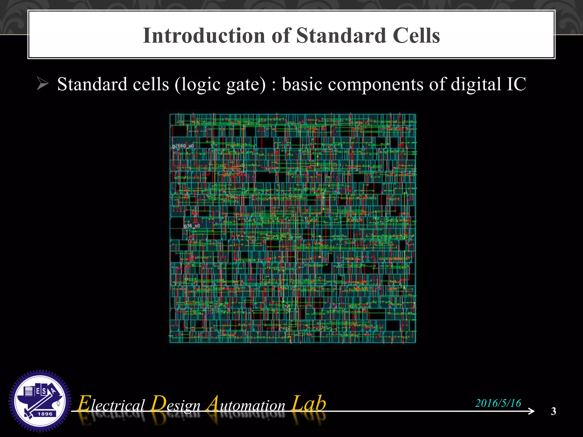
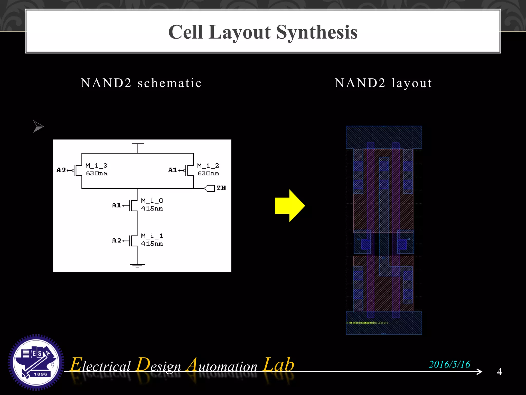
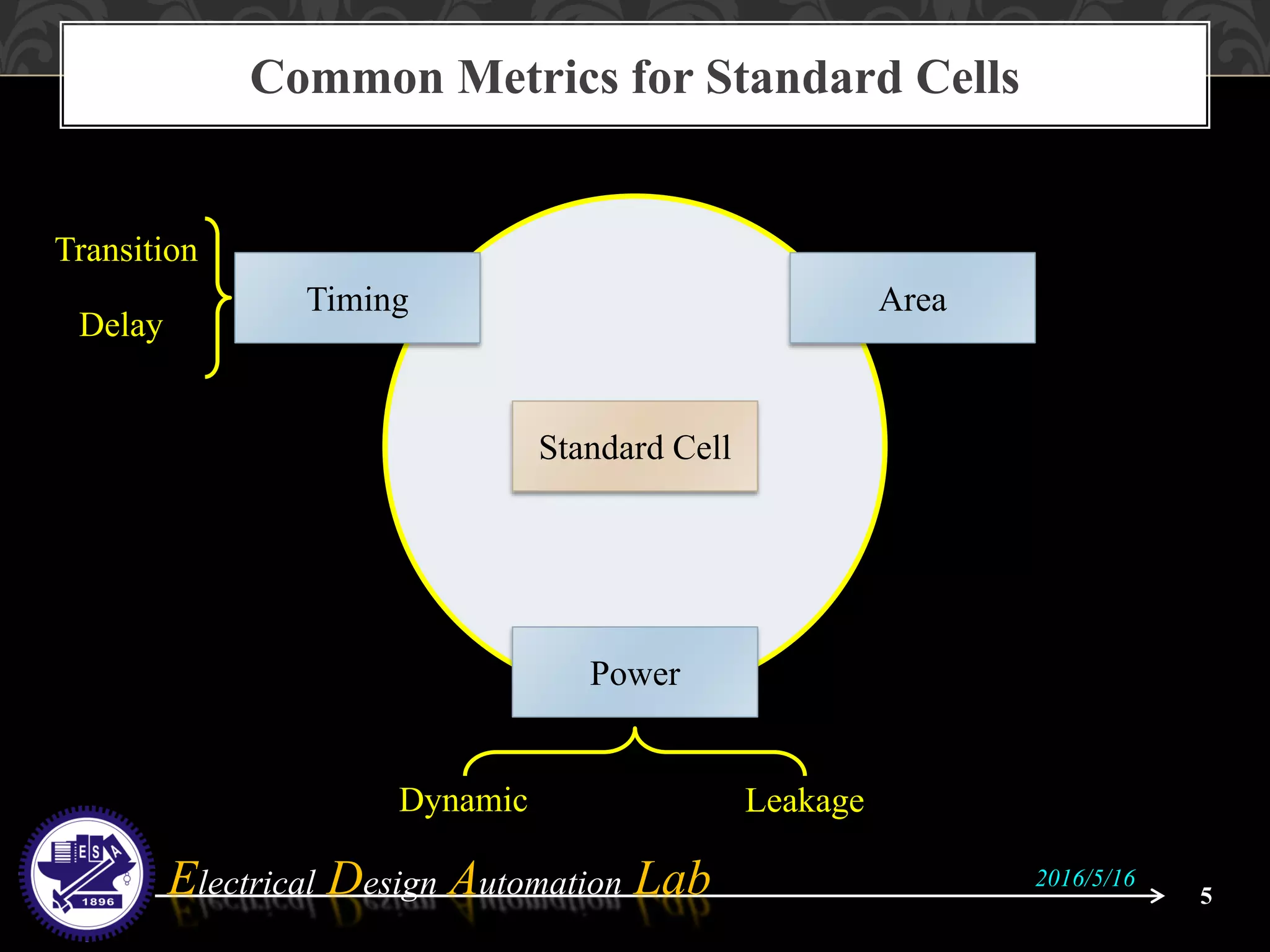
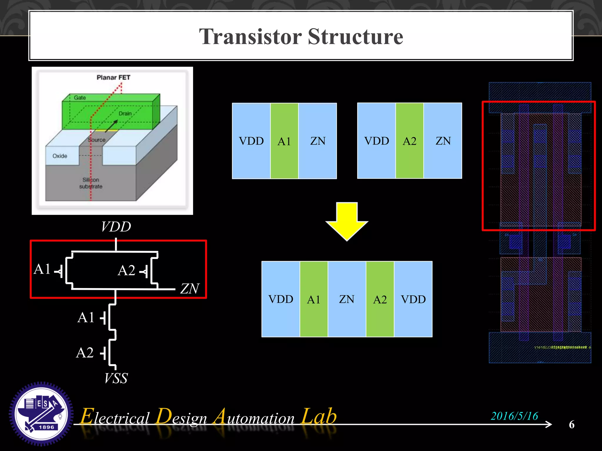
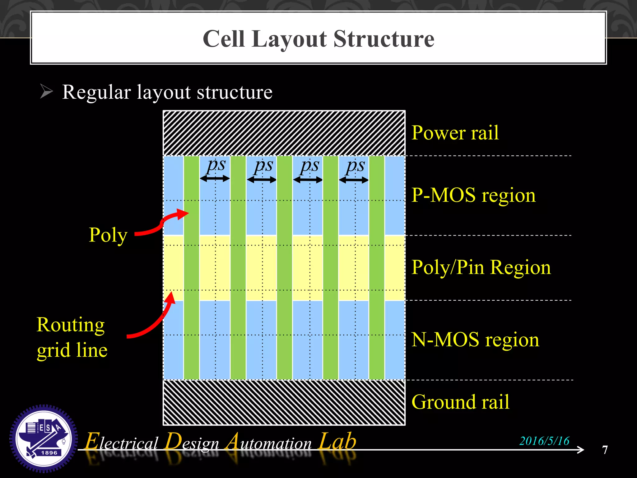
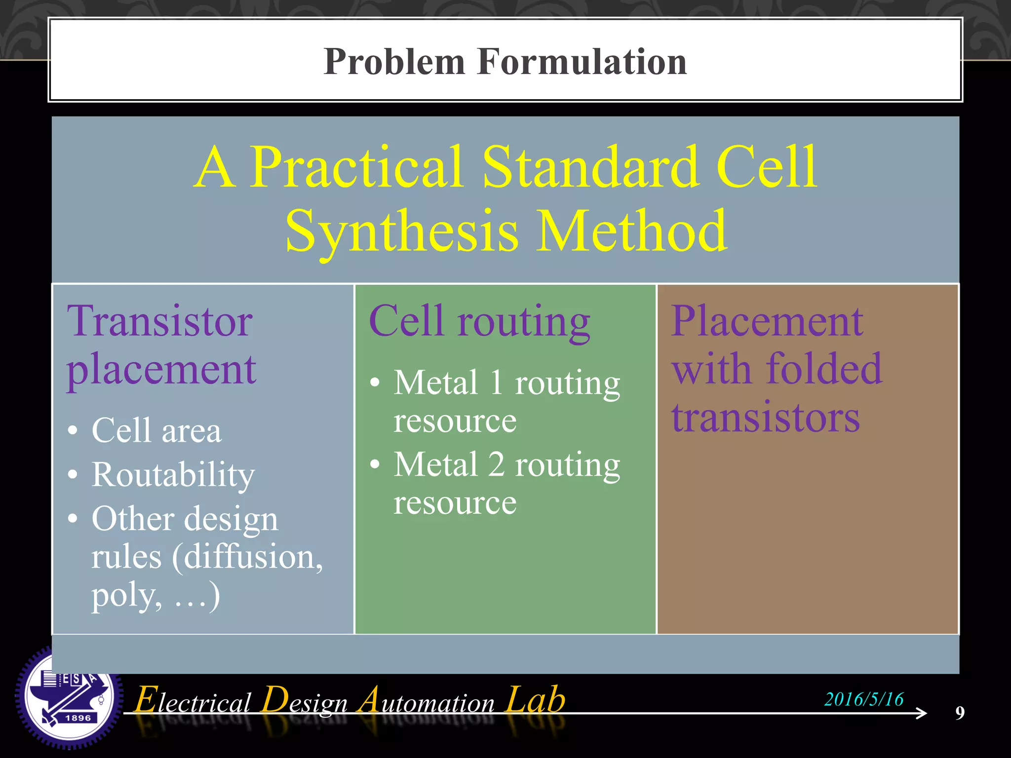
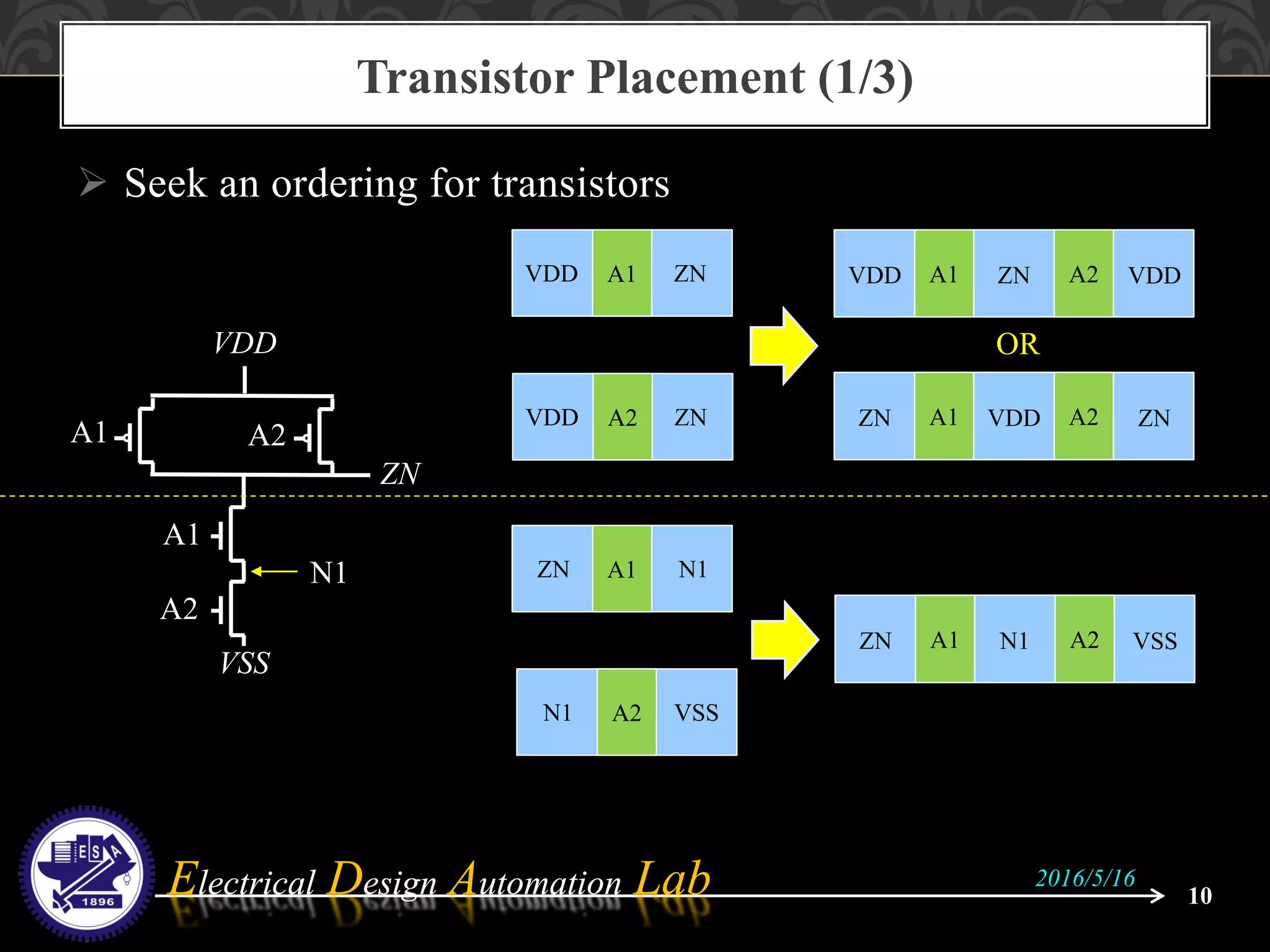
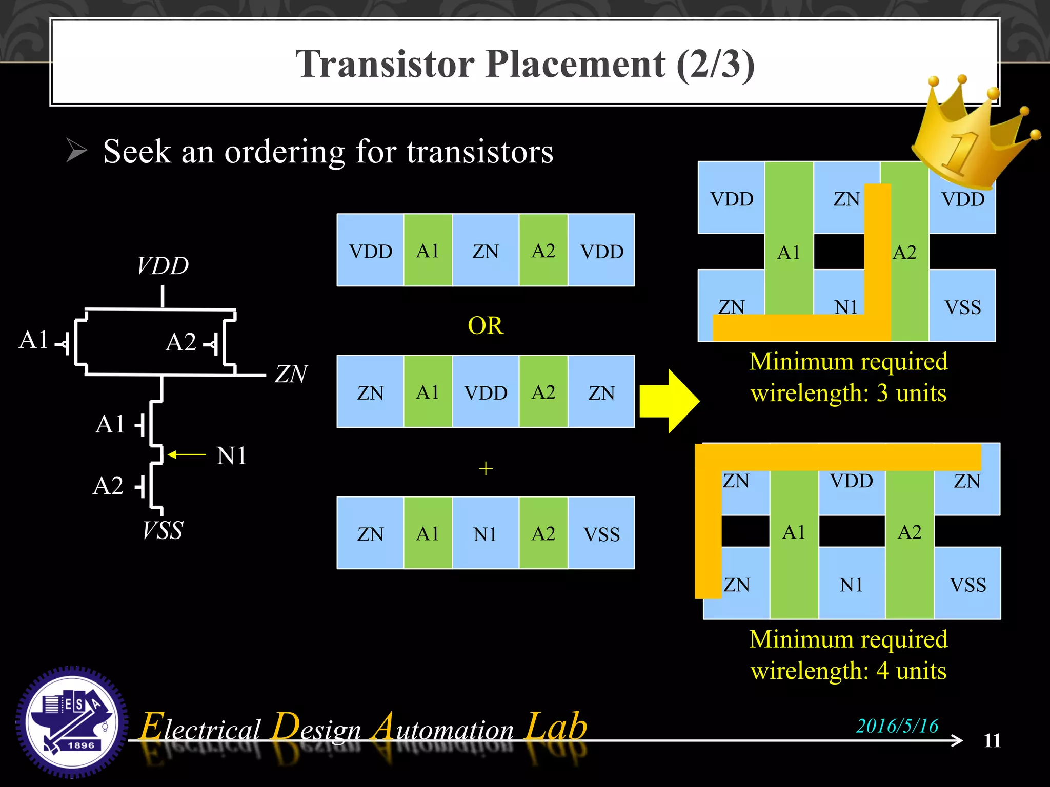
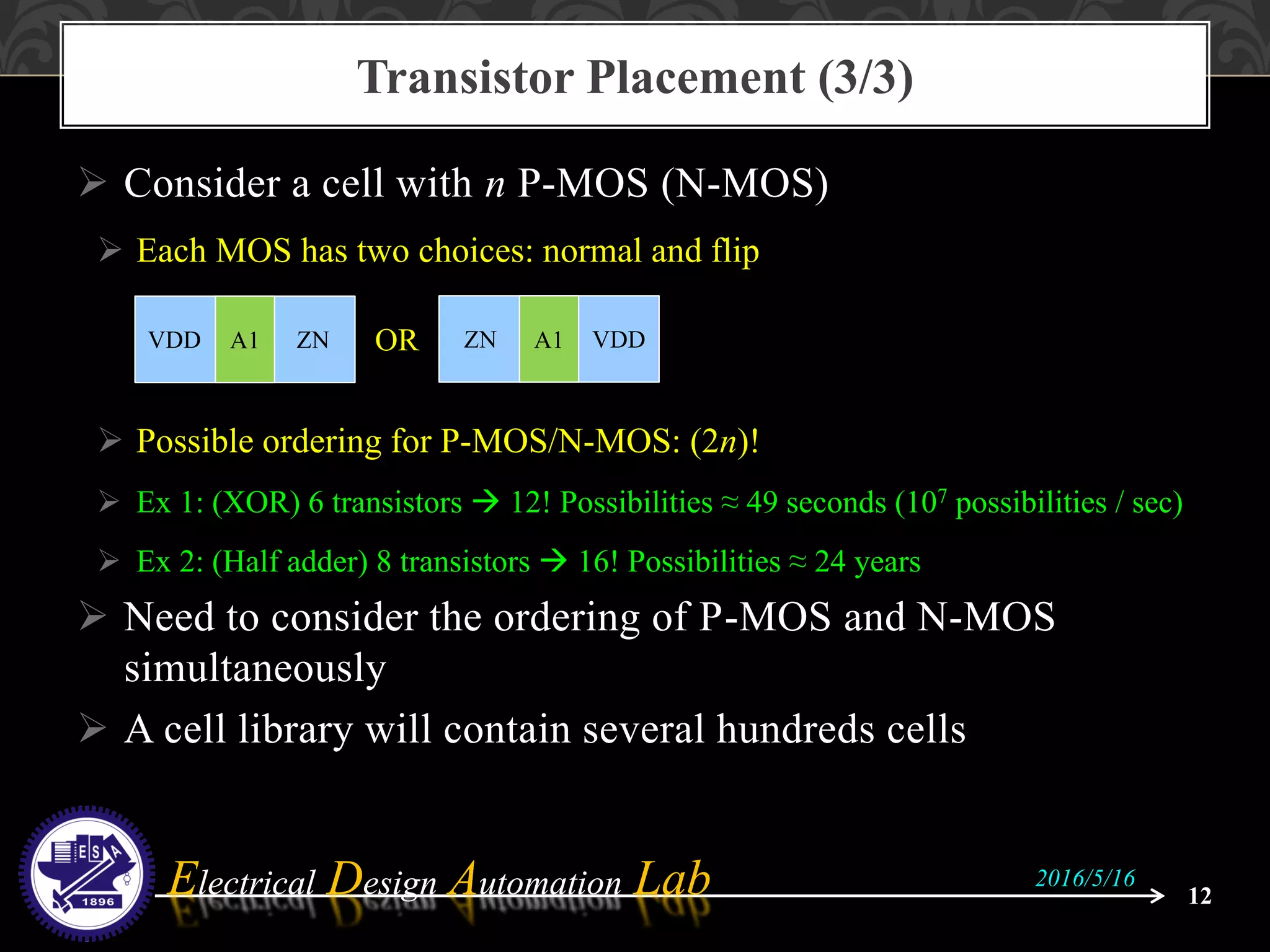
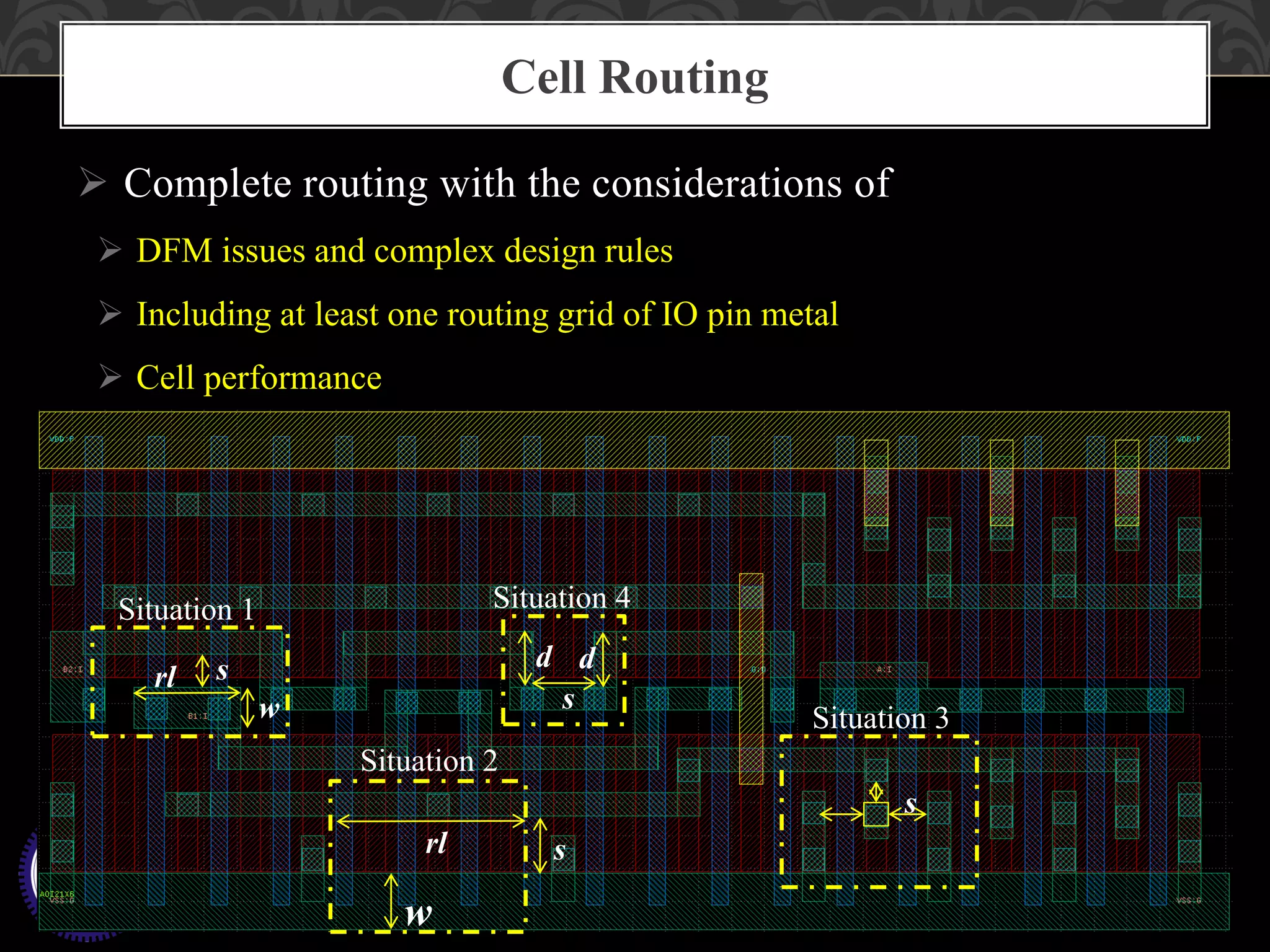
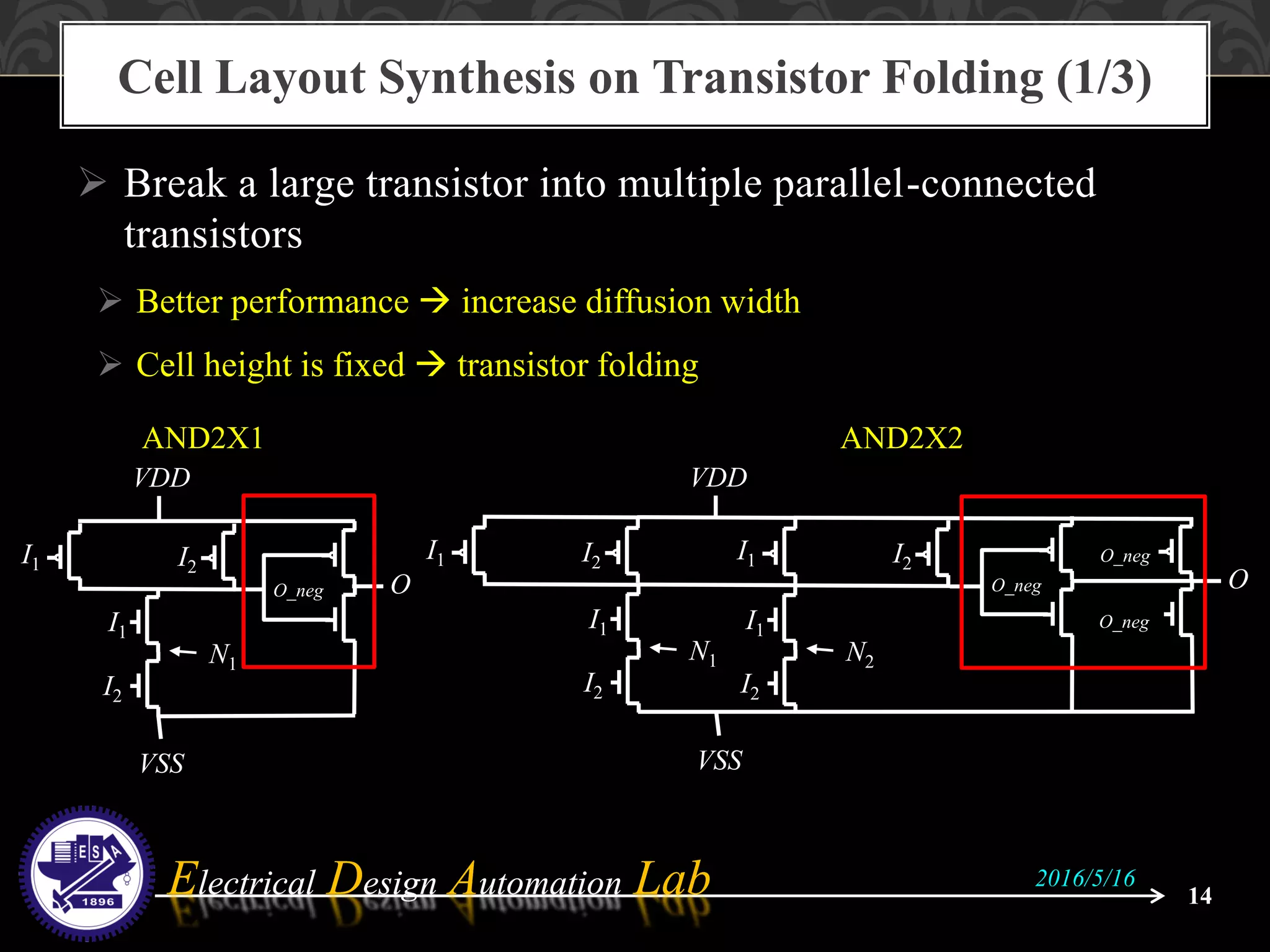
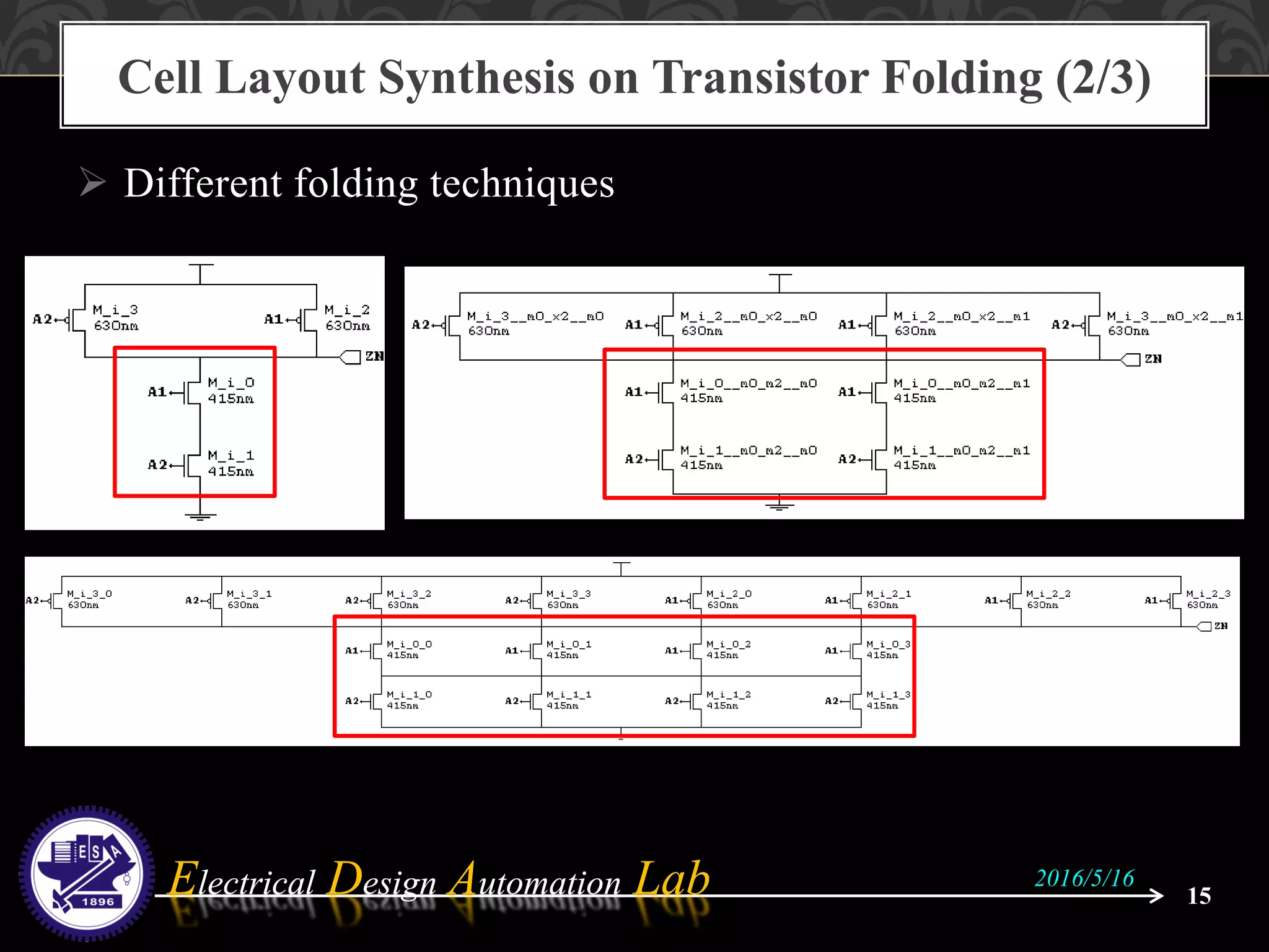
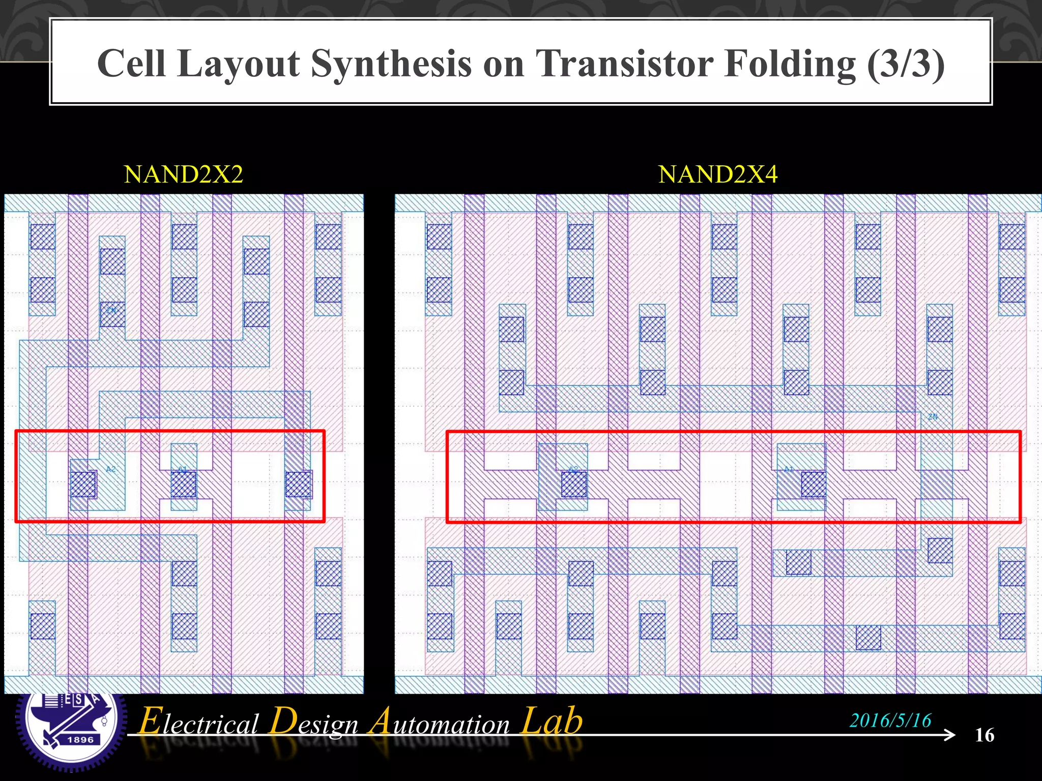
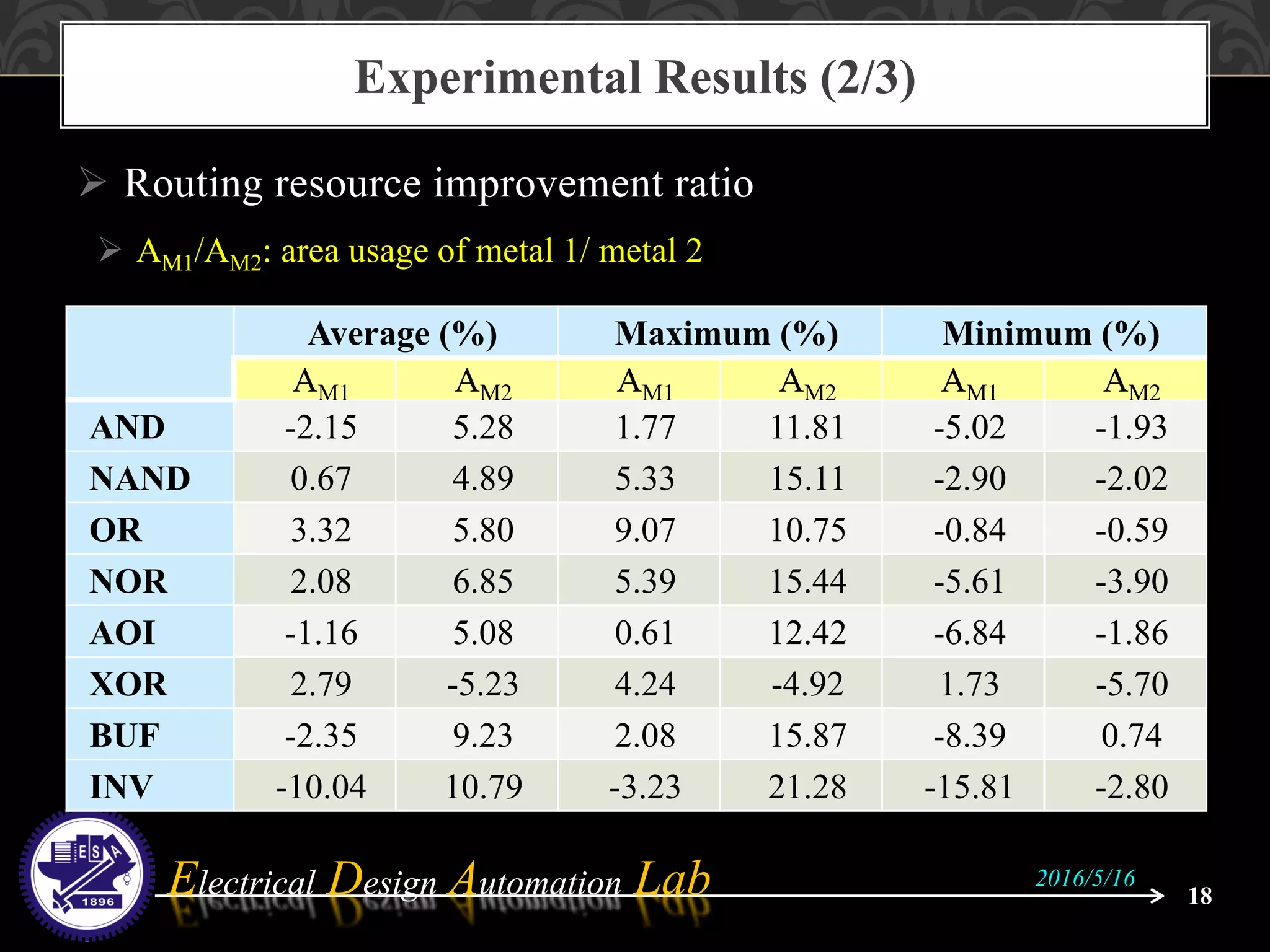
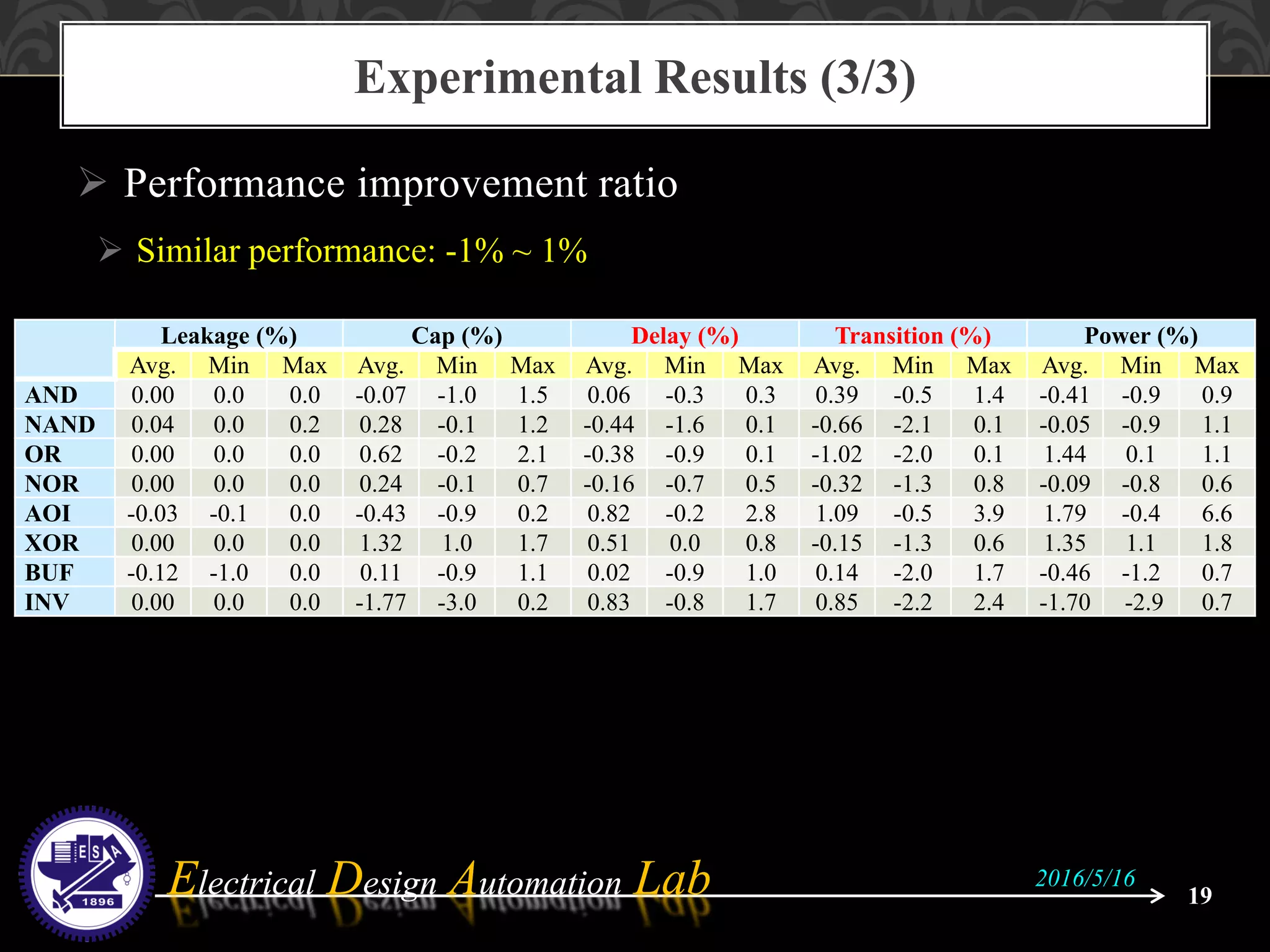
Electrical Design Automation Lab
Presenter: Hong-Yan Su (lionking)
Institute of Computer Science and Engineering
National Chiao Tung University
Design Challenges and Futures
High Performance Standard Cell Layout Synthesis for
Advanced Nanometer Technology Nodes
2016/5/16
1
Electrical Design Automation LabElectrical Design Automation Lab
 Introduction to standard cell basics
 Cell layout synthesis flow
 Transistor placement
 Cell routing
 Transistor folding
 Experimental results
 Future works
Outline
2
2016/5/16
Electrical Design Automation LabElectrical Design Automation Lab
 Standard cells (logic gate) : basic components of digital IC
Introduction of Standard Cells
3
2016/5/16
Electrical Design Automation Lab

NAND2 schematic NAND2 layout
Cell Layout Synthesis
4
2016/5/16
Electrical Design Automation Lab
Common Metrics for Standard Cells
5
2016/5/16
Standard Cell
AreaTiming
Power
Dynamic Leakage
Transition
Delay
Electrical Design Automation Lab
Transistor Structure
6
2016/5/16
A1VDD ZN A2VDD ZN
A1VDD A2ZN VDD
A1
VDD
ZN
VSS
A2
A1
A2
Electrical Design Automation LabElectrical Design Automation Lab
Power rail
Ground rail
P-MOS region
N-MOS region
Poly/Pin Region
Poly
ps ps ps ps
Routing
grid line
 Regular layout structure
Cell Layout Structure
7
2016/5/16
Electrical Design Automation LabElectrical Design Automation Lab
 A cell library contains several hundreds of standard cells
 One technology node will have several libraries for various purposes
 Determination on cell layout structure
 Complex and explosive number of design rules on advanced
technology nodes
Design Challenges on Standard Cell Library
8
2016/5/16
Electrical Design Automation Lab
Problem Formulation
9
2016/5/16
A Practical Standard Cell
Synthesis Method
Transistor
placement
• Cell area
• Routability
• Other design
rules (diffusion,
poly, …)
Cell routing
• Metal 1 routing
resource
• Metal 2 routing
resource
Placement
with folded
transistors
Electrical Design Automation LabElectrical Design Automation Lab
 Seek an ordering for transistors
Transistor Placement (1/3)
10
2016/5/16
A1VDD ZN
A2VDD ZN
A1VDD A2ZN VDD
A1ZN A2VDD ZN
OR
A1ZN N1
A2N1 VSS
A1ZN A2N1 VSS
A1
VDD
ZN
VSS
A2
A1
A2
N1
Electrical Design Automation LabElectrical Design Automation Lab
 Seek an ordering for transistors
Transistor Placement (2/3)
11
2016/5/16
A1ZN A2N1 VSS
A1
VDD
ZN
VSS
A2
A1
A2
N1
A1VDD A2ZN VDD
A1ZN A2VDD ZN
OR
+
VDD ZN VDD
ZN N1 VSS
A1 A2
ZN VDD ZN
A1
ZN
A2
N1 VSS
Minimum required
wirelength: 3 units
Minimum required
wirelength: 4 units
Electrical Design Automation LabElectrical Design Automation Lab
 Consider a cell with n P-MOS (N-MOS)
 Each MOS has two choices: normal and flip
 Possible ordering for P-MOS/N-MOS: (2n)!
 Ex 1: (XOR) 6 transistors  12! Possibilities ≈ 49 seconds (107 possibilities / sec)
 Ex 2: (Half adder) 8 transistors  16! Possibilities ≈ 24 years
 Need to consider the ordering of P-MOS and N-MOS
simultaneously
 A cell library will contain several hundreds cells
Transistor Placement (3/3)
12
2016/5/16
A1VDD ZN A1ZN VDDOR
Electrical Design Automation LabElectrical Design Automation Lab
 Complete routing with the considerations of
 DFM issues and complex design rules
 Including at least one routing grid of IO pin metal
 Cell performance
Cell Routing
13
2016/5/16
s
w
rl
Situation 1
Situation 2
rl
w
s
Situation 3
s
Situation 4
s
d d
Electrical Design Automation LabElectrical Design Automation Lab
 Break a large transistor into multiple parallel-connected
transistors
 Better performance  increase diffusion width
 Cell height is fixed  transistor folding
Cell Layout Synthesis on Transistor Folding (1/3)
14
2016/5/16
I1
VDD
O
I2
I1
I2
N1
VSS
O_neg
I1
VDD
I2
I1
I2
N1
I1 I2
I1
I2
N2
VSS
O_neg
O_neg
O_neg
O
AND2X1 AND2X2
Electrical Design Automation LabElectrical Design Automation Lab
 Different folding techniques
Cell Layout Synthesis on Transistor Folding (2/3)
15
2016/5/16
Electrical Design Automation Lab
Cell Layout Synthesis on Transistor Folding (3/3)
16
2016/5/16
NAND2X2 NAND2X4
Electrical Design Automation LabElectrical Design Automation Lab
 Environments
 Implemented with C++ on a Linux platform
 Intel-i7 3.4GHz CPU and 8 GB RAM
 Testcases: 28nm commercial technology node
 INV, BUF
 X1, X2, X3, X4, X6, X8, X12, X16, X20, X24, X32
 AND2, NAND2, OR2, NOR2, AOI12, XOR2
 X1, X2, X3, X4, X6, X8, X12, X16
 Comparison: with commercial standard cell library
 All the cases can be synthesized within 1 second with identical area
 Compute average/minimum/maximum improvement ratio of all driving
strengths
Experimental Results (1/3)
17
2016/5/16
Electrical Design Automation LabElectrical Design Automation Lab
Experimental Results (2/3)
18
2016/5/16
 Routing resource improvement ratio
 AM1/AM2: area usage of metal 1/ metal 2
Average (%) Maximum (%) Minimum (%)
AM1 AM2 AM1 AM2 AM1 AM2
AND -2.15 5.28 1.77 11.81 -5.02 -1.93
NAND 0.67 4.89 5.33 15.11 -2.90 -2.02
OR 3.32 5.80 9.07 10.75 -0.84 -0.59
NOR 2.08 6.85 5.39 15.44 -5.61 -3.90
AOI -1.16 5.08 0.61 12.42 -6.84 -1.86
XOR 2.79 -5.23 4.24 -4.92 1.73 -5.70
BUF -2.35 9.23 2.08 15.87 -8.39 0.74
INV -10.04 10.79 -3.23 21.28 -15.81 -2.80
Electrical Design Automation LabElectrical Design Automation Lab
 Performance improvement ratio
 Similar performance: -1% ~ 1%
Experimental Results (3/3)
19
2016/5/16
Leakage (%) Cap (%) Delay (%) Transition (%) Power (%)
Avg. Min Max Avg. Min Max Avg. Min Max Avg. Min Max Avg. Min Max
AND 0.00 0.0 0.0 -0.07 -1.0 1.5 0.06 -0.3 0.3 0.39 -0.5 1.4 -0.41 -0.9 0.9
NAND 0.04 0.0 0.2 0.28 -0.1 1.2 -0.44 -1.6 0.1 -0.66 -2.1 0.1 -0.05 -0.9 1.1
OR 0.00 0.0 0.0 0.62 -0.2 2.1 -0.38 -0.9 0.1 -1.02 -2.0 0.1 1.44 0.1 1.1
NOR 0.00 0.0 0.0 0.24 -0.1 0.7 -0.16 -0.7 0.5 -0.32 -1.3 0.8 -0.09 -0.8 0.6
AOI -0.03 -0.1 0.0 -0.43 -0.9 0.2 0.82 -0.2 2.8 1.09 -0.5 3.9 1.79 -0.4 6.6
XOR 0.00 0.0 0.0 1.32 1.0 1.7 0.51 0.0 0.8 -0.15 -1.3 0.6 1.35 1.1 1.8
BUF -0.12 -1.0 0.0 0.11 -0.9 1.1 0.02 -0.9 1.0 0.14 -2.0 1.7 -0.46 -1.2 0.7
INV 0.00 0.0 0.0 -1.77 -3.0 0.2 0.83 -0.8 1.7 0.85 -2.2 2.4 -1.70 -2.9 0.7
Electrical Design Automation LabElectrical Design Automation Lab
 Routability estimation on transistor placement
 Smaller the better? No!
 DFM-related issues
 Multiple patterning
 Direct-self Assembly (DSA)
 New MOS structure
 FinFET / Gate all around / …
 Cell layout design aspect considering whole chip APR
 Smaller the better? No!
Future Works
20
2016/5/16

High performance standard cell layout synthesis for advanced nanometer

  • 1.
    Electrical Design AutomationLab Presenter: Hong-Yan Su (lionking) Institute of Computer Science and Engineering National Chiao Tung University Design Challenges and Futures High Performance Standard Cell Layout Synthesis for Advanced Nanometer Technology Nodes 2016/5/16 1
  • 2.
    Electrical Design AutomationLabElectrical Design Automation Lab  Introduction to standard cell basics  Cell layout synthesis flow  Transistor placement  Cell routing  Transistor folding  Experimental results  Future works Outline 2 2016/5/16
  • 3.
    Electrical Design AutomationLabElectrical Design Automation Lab  Standard cells (logic gate) : basic components of digital IC Introduction of Standard Cells 3 2016/5/16
  • 4.
    Electrical Design AutomationLab  NAND2 schematic NAND2 layout Cell Layout Synthesis 4 2016/5/16
  • 5.
    Electrical Design AutomationLab Common Metrics for Standard Cells 5 2016/5/16 Standard Cell AreaTiming Power Dynamic Leakage Transition Delay
  • 6.
    Electrical Design AutomationLab Transistor Structure 6 2016/5/16 A1VDD ZN A2VDD ZN A1VDD A2ZN VDD A1 VDD ZN VSS A2 A1 A2
  • 7.
    Electrical Design AutomationLabElectrical Design Automation Lab Power rail Ground rail P-MOS region N-MOS region Poly/Pin Region Poly ps ps ps ps Routing grid line  Regular layout structure Cell Layout Structure 7 2016/5/16
  • 8.
    Electrical Design AutomationLabElectrical Design Automation Lab  A cell library contains several hundreds of standard cells  One technology node will have several libraries for various purposes  Determination on cell layout structure  Complex and explosive number of design rules on advanced technology nodes Design Challenges on Standard Cell Library 8 2016/5/16
  • 9.
    Electrical Design AutomationLab Problem Formulation 9 2016/5/16 A Practical Standard Cell Synthesis Method Transistor placement • Cell area • Routability • Other design rules (diffusion, poly, …) Cell routing • Metal 1 routing resource • Metal 2 routing resource Placement with folded transistors
  • 10.
    Electrical Design AutomationLabElectrical Design Automation Lab  Seek an ordering for transistors Transistor Placement (1/3) 10 2016/5/16 A1VDD ZN A2VDD ZN A1VDD A2ZN VDD A1ZN A2VDD ZN OR A1ZN N1 A2N1 VSS A1ZN A2N1 VSS A1 VDD ZN VSS A2 A1 A2 N1
  • 11.
    Electrical Design AutomationLabElectrical Design Automation Lab  Seek an ordering for transistors Transistor Placement (2/3) 11 2016/5/16 A1ZN A2N1 VSS A1 VDD ZN VSS A2 A1 A2 N1 A1VDD A2ZN VDD A1ZN A2VDD ZN OR + VDD ZN VDD ZN N1 VSS A1 A2 ZN VDD ZN A1 ZN A2 N1 VSS Minimum required wirelength: 3 units Minimum required wirelength: 4 units
  • 12.
    Electrical Design AutomationLabElectrical Design Automation Lab  Consider a cell with n P-MOS (N-MOS)  Each MOS has two choices: normal and flip  Possible ordering for P-MOS/N-MOS: (2n)!  Ex 1: (XOR) 6 transistors  12! Possibilities ≈ 49 seconds (107 possibilities / sec)  Ex 2: (Half adder) 8 transistors  16! Possibilities ≈ 24 years  Need to consider the ordering of P-MOS and N-MOS simultaneously  A cell library will contain several hundreds cells Transistor Placement (3/3) 12 2016/5/16 A1VDD ZN A1ZN VDDOR
  • 13.
    Electrical Design AutomationLabElectrical Design Automation Lab  Complete routing with the considerations of  DFM issues and complex design rules  Including at least one routing grid of IO pin metal  Cell performance Cell Routing 13 2016/5/16 s w rl Situation 1 Situation 2 rl w s Situation 3 s Situation 4 s d d
  • 14.
    Electrical Design AutomationLabElectrical Design Automation Lab  Break a large transistor into multiple parallel-connected transistors  Better performance  increase diffusion width  Cell height is fixed  transistor folding Cell Layout Synthesis on Transistor Folding (1/3) 14 2016/5/16 I1 VDD O I2 I1 I2 N1 VSS O_neg I1 VDD I2 I1 I2 N1 I1 I2 I1 I2 N2 VSS O_neg O_neg O_neg O AND2X1 AND2X2
  • 15.
    Electrical Design AutomationLabElectrical Design Automation Lab  Different folding techniques Cell Layout Synthesis on Transistor Folding (2/3) 15 2016/5/16
  • 16.
    Electrical Design AutomationLab Cell Layout Synthesis on Transistor Folding (3/3) 16 2016/5/16 NAND2X2 NAND2X4
  • 17.
    Electrical Design AutomationLabElectrical Design Automation Lab  Environments  Implemented with C++ on a Linux platform  Intel-i7 3.4GHz CPU and 8 GB RAM  Testcases: 28nm commercial technology node  INV, BUF  X1, X2, X3, X4, X6, X8, X12, X16, X20, X24, X32  AND2, NAND2, OR2, NOR2, AOI12, XOR2  X1, X2, X3, X4, X6, X8, X12, X16  Comparison: with commercial standard cell library  All the cases can be synthesized within 1 second with identical area  Compute average/minimum/maximum improvement ratio of all driving strengths Experimental Results (1/3) 17 2016/5/16
  • 18.
    Electrical Design AutomationLabElectrical Design Automation Lab Experimental Results (2/3) 18 2016/5/16  Routing resource improvement ratio  AM1/AM2: area usage of metal 1/ metal 2 Average (%) Maximum (%) Minimum (%) AM1 AM2 AM1 AM2 AM1 AM2 AND -2.15 5.28 1.77 11.81 -5.02 -1.93 NAND 0.67 4.89 5.33 15.11 -2.90 -2.02 OR 3.32 5.80 9.07 10.75 -0.84 -0.59 NOR 2.08 6.85 5.39 15.44 -5.61 -3.90 AOI -1.16 5.08 0.61 12.42 -6.84 -1.86 XOR 2.79 -5.23 4.24 -4.92 1.73 -5.70 BUF -2.35 9.23 2.08 15.87 -8.39 0.74 INV -10.04 10.79 -3.23 21.28 -15.81 -2.80
  • 19.
    Electrical Design AutomationLabElectrical Design Automation Lab  Performance improvement ratio  Similar performance: -1% ~ 1% Experimental Results (3/3) 19 2016/5/16 Leakage (%) Cap (%) Delay (%) Transition (%) Power (%) Avg. Min Max Avg. Min Max Avg. Min Max Avg. Min Max Avg. Min Max AND 0.00 0.0 0.0 -0.07 -1.0 1.5 0.06 -0.3 0.3 0.39 -0.5 1.4 -0.41 -0.9 0.9 NAND 0.04 0.0 0.2 0.28 -0.1 1.2 -0.44 -1.6 0.1 -0.66 -2.1 0.1 -0.05 -0.9 1.1 OR 0.00 0.0 0.0 0.62 -0.2 2.1 -0.38 -0.9 0.1 -1.02 -2.0 0.1 1.44 0.1 1.1 NOR 0.00 0.0 0.0 0.24 -0.1 0.7 -0.16 -0.7 0.5 -0.32 -1.3 0.8 -0.09 -0.8 0.6 AOI -0.03 -0.1 0.0 -0.43 -0.9 0.2 0.82 -0.2 2.8 1.09 -0.5 3.9 1.79 -0.4 6.6 XOR 0.00 0.0 0.0 1.32 1.0 1.7 0.51 0.0 0.8 -0.15 -1.3 0.6 1.35 1.1 1.8 BUF -0.12 -1.0 0.0 0.11 -0.9 1.1 0.02 -0.9 1.0 0.14 -2.0 1.7 -0.46 -1.2 0.7 INV 0.00 0.0 0.0 -1.77 -3.0 0.2 0.83 -0.8 1.7 0.85 -2.2 2.4 -1.70 -2.9 0.7
  • 20.
    Electrical Design AutomationLabElectrical Design Automation Lab  Routability estimation on transistor placement  Smaller the better? No!  DFM-related issues  Multiple patterning  Direct-self Assembly (DSA)  New MOS structure  FinFET / Gate all around / …  Cell layout design aspect considering whole chip APR  Smaller the better? No! Future Works 20 2016/5/16