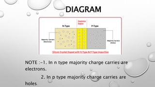
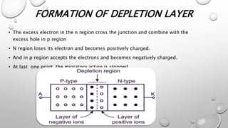
CONTENT
INTRODUCTION
DIAGRAM
CHARGE CARRIERS
FORMATION OF DEPLETION LAYER
DIFFUSION CURRENT AND DRIFT CURRENT
CONCLUSION
INTRODUCTION
• A P-N junction is a device formed by joining by p-type(doped with B ,Al) with n-
types doped with (P ,As ,Sb) semiconductor and separated by an thin junction is
called p-n junction diode or junction diode.
• The plane dividing the two zones is called junction (plane lies where density of
donors and acceptors is equal)
• The three phenomena takes place at junction
1. Depletion layer
2. Barrier potential
3. Diffusion capacitance
DIAGRAM
NOTE :-1. In n type majority charge carries are
electrons.
2. In p type majority charge carries are
holes.
CHARGE CARRIERS
In p-n junction
• On the n side, the electrons are the majority carriers, while the holes are
the minority carriers.
• Near the junction is a region having no free charge carriers. This region,
called the depletion layer, behaves as an insulator.
• We can also denote p as a anode and n as a cathode that is
+ve and –ve.
FORMATION OF DEPLETION LAYER
• The excess electron in the n region cross the junction and combine with the
excess hole in p region
• N region loses its electron and becomes positively charged.
• And in p region accepts the electrons and becomes negatively charged.
• At last one point ,the migratory action is stopped.
DIFFUSION CURRENT AND DRIFT CURRENT
• Diffusion current is due to concentration gradient of charge carriers across the
junction and it is due to majority charge carriers. So it means, diffusion current is
due to movement of holes from p side to n side.
• Movement of electrons and holes to the positive layers and negative layers is
formation of current that current is called drift current.
• The direction of current in diffusion is just opposite of drift.
CONCLUSION
• The p-n junction is the basics building block for semiconductor device . understanding of
junction theory serve as the foundation to understanding other semiconductor devices.
• When positive applied to the p side large currents will flow through junction while , when
negative applied virtually no currents flow.
• Modern p n junction are fabricated using planar technology.
• Biasing play vital role in p n semiconductor device.
formation_of_pn_juction.pptx

formation_of_pn_juction.pptx

  • 2.
    CONTENT INTRODUCTION DIAGRAM CHARGE CARRIERS FORMATION OFDEPLETION LAYER DIFFUSION CURRENT AND DRIFT CURRENT CONCLUSION
  • 3.
    INTRODUCTION • A P-Njunction is a device formed by joining by p-type(doped with B ,Al) with n- types doped with (P ,As ,Sb) semiconductor and separated by an thin junction is called p-n junction diode or junction diode. • The plane dividing the two zones is called junction (plane lies where density of donors and acceptors is equal) • The three phenomena takes place at junction 1. Depletion layer 2. Barrier potential 3. Diffusion capacitance
  • 4.
    DIAGRAM NOTE :-1. Inn type majority charge carries are electrons. 2. In p type majority charge carries are holes.
  • 5.
    CHARGE CARRIERS In p-njunction • On the n side, the electrons are the majority carriers, while the holes are the minority carriers. • Near the junction is a region having no free charge carriers. This region, called the depletion layer, behaves as an insulator. • We can also denote p as a anode and n as a cathode that is +ve and –ve.
  • 6.
    FORMATION OF DEPLETIONLAYER • The excess electron in the n region cross the junction and combine with the excess hole in p region • N region loses its electron and becomes positively charged. • And in p region accepts the electrons and becomes negatively charged. • At last one point ,the migratory action is stopped.
  • 7.
    DIFFUSION CURRENT ANDDRIFT CURRENT • Diffusion current is due to concentration gradient of charge carriers across the junction and it is due to majority charge carriers. So it means, diffusion current is due to movement of holes from p side to n side. • Movement of electrons and holes to the positive layers and negative layers is formation of current that current is called drift current. • The direction of current in diffusion is just opposite of drift.
  • 8.
    CONCLUSION • The p-njunction is the basics building block for semiconductor device . understanding of junction theory serve as the foundation to understanding other semiconductor devices. • When positive applied to the p side large currents will flow through junction while , when negative applied virtually no currents flow. • Modern p n junction are fabricated using planar technology. • Biasing play vital role in p n semiconductor device.