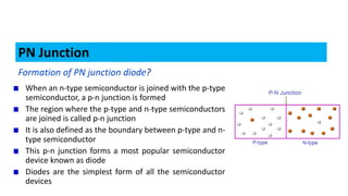
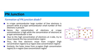
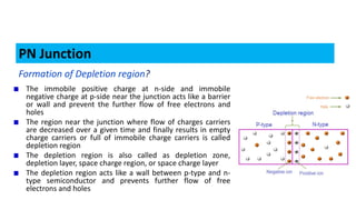
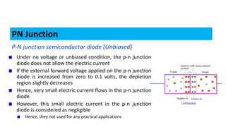
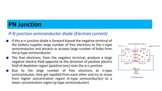
When a p-type and n-type semiconductor are joined, electrons flow from the n-side to the p-side, leaving positive ions in the n-side and negative ions in the p-side. This forms an electric field called a depletion region that acts as a barrier. When a voltage is applied in the forward direction, it reduces the depletion region, allowing electrons and holes to flow more easily across the junction. This forms the basis of a p-n junction diode, which allows current to flow easily in one direction but blocks it in the other.
The Zener diode is a heavily doped diode which, as a result of doping, has a very narrow depletion region. This allows the diode to be operated in the reverse biased region of the characteristic curve without damaging the PN junction.
“Zener Effect”: The area of Zener diode operation (<5V) where the Diode maintains a constant voltage output while operating reverse biased.
“Avalanche Effect”: >5V applied to the diode while reverse biased which tends to cause the diode to eventually breakdown due to heat generation within the lattice structure of the crystal.
Because of its higher temperature and current capability, silicon is usually preferred in manufacture of Zener Diodes
Zener Diodes provide a stable reference voltage for use in power supplies, voltmeter & other instruments, voltage regulators.
CW RADAR, FMCW RADAR, FMCW ALTIMETER, AND THEIR PARAMETERSveerababupersonal22
It consists of cw radar and fmcw radar ,range measurement,if amplifier and fmcw altimeterThe CW radar operates using continuous wave transmission, while the FMCW radar employs frequency-modulated continuous wave technology. Range measurement is a crucial aspect of radar systems, providing information about the distance to a target. The IF amplifier plays a key role in signal processing, amplifying intermediate frequency signals for further analysis. The FMCW altimeter utilizes frequency-modulated continuous wave technology to accurately measure altitude above a reference point.
Overview of the fundamental roles in Hydropower generation and the components involved in wider Electrical Engineering.
This paper presents the design and construction of hydroelectric dams from the hydrologist’s survey of the valley before construction, all aspects and involved disciplines, fluid dynamics, structural engineering, generation and mains frequency regulation to the very transmission of power through the network in the United Kingdom.
Author: Robbie Edward Sayers
Collaborators and co editors: Charlie Sims and Connor Healey.
(C) 2024 Robbie E. Sayers
Hybrid optimization of pumped hydro system and solar- Engr. Abdul-Azeez.pdffxintegritypublishin
Advancements in technology unveil a myriad of electrical and electronic breakthroughs geared towards efficiently harnessing limited resources to meet human energy demands. The optimization of hybrid solar PV panels and pumped hydro energy supply systems plays a pivotal role in utilizing natural resources effectively. This initiative not only benefits humanity but also fosters environmental sustainability. The study investigated the design optimization of these hybrid systems, focusing on understanding solar radiation patterns, identifying geographical influences on solar radiation, formulating a mathematical model for system optimization, and determining the optimal configuration of PV panels and pumped hydro storage. Through a comparative analysis approach and eight weeks of data collection, the study addressed key research questions related to solar radiation patterns and optimal system design. The findings highlighted regions with heightened solar radiation levels, showcasing substantial potential for power generation and emphasizing the system's efficiency. Optimizing system design significantly boosted power generation, promoted renewable energy utilization, and enhanced energy storage capacity. The study underscored the benefits of optimizing hybrid solar PV panels and pumped hydro energy supply systems for sustainable energy usage. Optimizing the design of solar PV panels and pumped hydro energy supply systems as examined across diverse climatic conditions in a developing country, not only enhances power generation but also improves the integration of renewable energy sources and boosts energy storage capacities, particularly beneficial for less economically prosperous regions. Additionally, the study provides valuable insights for advancing energy research in economically viable areas. Recommendations included conducting site-specific assessments, utilizing advanced modeling tools, implementing regular maintenance protocols, and enhancing communication among system components.
NO1 Uk best vashikaran specialist in delhi vashikaran baba near me online vas...Amil Baba Dawood bangali
Contact with Dawood Bhai Just call on +92322-6382012 and we'll help you. We'll solve all your problems within 12 to 24 hours and with 101% guarantee and with astrology systematic. If you want to take any personal or professional advice then also you can call us on +92322-6382012 , ONLINE LOVE PROBLEM & Other all types of Daily Life Problem's.Then CALL or WHATSAPP us on +92322-6382012 and Get all these problems solutions here by Amil Baba DAWOOD BANGALI
#vashikaranspecialist #astrologer #palmistry #amliyaat #taweez #manpasandshadi #horoscope #spiritual #lovelife #lovespell #marriagespell#aamilbabainpakistan #amilbabainkarachi #powerfullblackmagicspell #kalajadumantarspecialist #realamilbaba #AmilbabainPakistan #astrologerincanada #astrologerindubai #lovespellsmaster #kalajaduspecialist #lovespellsthatwork #aamilbabainlahore#blackmagicformarriage #aamilbaba #kalajadu #kalailam #taweez #wazifaexpert #jadumantar #vashikaranspecialist #astrologer #palmistry #amliyaat #taweez #manpasandshadi #horoscope #spiritual #lovelife #lovespell #marriagespell#aamilbabainpakistan #amilbabainkarachi #powerfullblackmagicspell #kalajadumantarspecialist #realamilbaba #AmilbabainPakistan #astrologerincanada #astrologerindubai #lovespellsmaster #kalajaduspecialist #lovespellsthatwork #aamilbabainlahore #blackmagicforlove #blackmagicformarriage #aamilbaba #kalajadu #kalailam #taweez #wazifaexpert #jadumantar #vashikaranspecialist #astrologer #palmistry #amliyaat #taweez #manpasandshadi #horoscope #spiritual #lovelife #lovespell #marriagespell#aamilbabainpakistan #amilbabainkarachi #powerfullblackmagicspell #kalajadumantarspecialist #realamilbaba #AmilbabainPakistan #astrologerincanada #astrologerindubai #lovespellsmaster #kalajaduspecialist #lovespellsthatwork #aamilbabainlahore #Amilbabainuk #amilbabainspain #amilbabaindubai #Amilbabainnorway #amilbabainkrachi #amilbabainlahore #amilbabaingujranwalan #amilbabainislamabad
Immunizing Image Classifiers Against Localized Adversary Attacksgerogepatton
This paper addresses the vulnerability of deep learning models, particularly convolutional neural networks
(CNN)s, to adversarial attacks and presents a proactive training technique designed to counter them. We
introduce a novel volumization algorithm, which transforms 2D images into 3D volumetric representations.
When combined with 3D convolution and deep curriculum learning optimization (CLO), itsignificantly improves
the immunity of models against localized universal attacks by up to 40%. We evaluate our proposed approach
using contemporary CNN architectures and the modified Canadian Institute for Advanced Research (CIFAR-10
and CIFAR-100) and ImageNet Large Scale Visual Recognition Challenge (ILSVRC12) datasets, showcasing
accuracy improvements over previous techniques. The results indicate that the combination of the volumetric
input and curriculum learning holds significant promise for mitigating adversarial attacks without necessitating
adversary training.
Cosmetic shop management system project report.pdfKamal Acharya
Buying new cosmetic products is difficult. It can even be scary for those who have sensitive skin and are prone to skin trouble. The information needed to alleviate this problem is on the back of each product, but it's thought to interpret those ingredient lists unless you have a background in chemistry.
Instead of buying and hoping for the best, we can use data science to help us predict which products may be good fits for us. It includes various function programs to do the above mentioned tasks.
Data file handling has been effectively used in the program.
The automated cosmetic shop management system should deal with the automation of general workflow and administration process of the shop. The main processes of the system focus on customer's request where the system is able to search the most appropriate products and deliver it to the customers. It should help the employees to quickly identify the list of cosmetic product that have reached the minimum quantity and also keep a track of expired date for each cosmetic product. It should help the employees to find the rack number in which the product is placed.It is also Faster and more efficient way.
We have compiled the most important slides from each speaker's presentation. This year’s compilation, available for free, captures the key insights and contributions shared during the DfMAy 2024 conference.
Final project report on grocery store management system..pdfKamal Acharya
In today’s fast-changing business environment, it’s extremely important to be able to respond to client needs in the most effective and timely manner. If your customers wish to see your business online and have instant access to your products or services.
Online Grocery Store is an e-commerce website, which retails various grocery products. This project allows viewing various products available enables registered users to purchase desired products instantly using Paytm, UPI payment processor (Instant Pay) and also can place order by using Cash on Delivery (Pay Later) option. This project provides an easy access to Administrators and Managers to view orders placed using Pay Later and Instant Pay options.
In order to develop an e-commerce website, a number of Technologies must be studied and understood. These include multi-tiered architecture, server and client-side scripting techniques, implementation technologies, programming language (such as PHP, HTML, CSS, JavaScript) and MySQL relational databases. This is a project with the objective to develop a basic website where a consumer is provided with a shopping cart website and also to know about the technologies used to develop such a website.
This document will discuss each of the underlying technologies to create and implement an e- commerce website.
6th International Conference on Machine Learning & Applications (CMLA 2024)ClaraZara1
6th International Conference on Machine Learning & Applications (CMLA 2024) will provide an excellent international forum for sharing knowledge and results in theory, methodology and applications of on Machine Learning & Applications.
Saudi Arabia stands as a titan in the global energy landscape, renowned for its abundant oil and gas resources. It's the largest exporter of petroleum and holds some of the world's most significant reserves. Let's delve into the top 10 oil and gas projects shaping Saudi Arabia's energy future in 2024.
2. PN Junction
Formation of PN junction diode?
Before the invention of semiconductor diode there was vacuum tubes which are large
in size, takes more power, costly, and noisy
This problem was solved with invention of semiconductor diode
Semiconductor diodes are small in size, low cost and consume less power
3. PN Junction
Formation of PN junction diode?
In n-type semiconductors electrons are the majority carriers while holes are minority
carriers
In p-type semiconductors holes are the majority carriers while electrons are minority
carriers
The p-type and n-type semiconductors are not used separately for practical purpose
because the overall charge of p-type and n-type semiconductors is electrically neutral
However, when p-type and n-type semiconductor materials are joined they behave
differently
4. PN Junction
Formation of PN junction diode?
When an n-type semiconductor is joined with the p-type
semiconductor, a p-n junction is formed
The region where the p-type and n-type semiconductors
are joined is called p-n junction
It is also defined as the boundary between p-type and n-
type semiconductor
This p-n junction forms a most popular semiconductor
device known as diode
Diodes are the simplest form of all the semiconductor
devices
5. PN Junction
Formation of PN junction diode?
In n-type semiconductor large number of free electrons is
present while at p-type semiconductor small number of free
electrons is present
Hence, the concentration of electrons at n-type
semiconductor is high while the concentration of electrons at
p-type semiconductor is low
Due to this high concentration of electrons at n-side, try to
move towards the low concentration region
Thus, the free electrons move from n-region (high
concentration region) to p-region (low concentration region)
Similarly, the holes move from p-region (high concentration
region) to n-region (low concentration region
6. PN Junction
Formation of Barrier Voltage?
The free electrons crossing the junction provide the extra
electrons to the p-side atoms by filling the holes in the p-side
atoms
The when atom which gains extra electron or lose electron
become a negative ion
Thus, each free electron that crosses the junction to fill the
holes in the p-side creates negative ions on the p-side
Similarly, each free electron that crosses the junction to fill
the holes in the p-side creates positive ions on the n-side
Positive ions are also called as donors because they donate
extra electrons to the outside atoms while negative ions are
called acceptors
7. PN Junction
Formation of Barrier Voltage?
Thus, a net positive charge is built at the n-side of the p-n junction
due to the positive ions at the n-side
similarly a net negative charge is built at the p-side of the p-n
junction due to the negative ions at the p-side
This net negative charge at the p-side of the p-n junction prevents
the further flow of free electrons crossing from n-side to p-side
Because the negative charge present at the p-side of p-n junction repels
the free electrons
Similarly, the net positive charge at n-side of the p-n junction
prevents the further flow of holes crossing from p-side to n-side
Hence, positive charge present at n-side and negative charge
present at p-side of p-n junction acts as barrier between p-type and
n-type semiconductor
8. PN Junction
Formation of Barrier Voltage?
The electric potential that occurs due to total charge
formed at the p-n junction is called barrier voltage,
barrier potential or junction barrier
The size of the barrier voltage at the p-n junction
depends on, the amount of doping, junction
temperature and type of material used
The barrier voltage for silicon diode is 0.7 volts and for
germanium is 0.3 volts
10. PN Junction
Formation of Barrier Voltage?
The barrier voltage allows the flow of minority charge carriers
Any free electrons (minority carriers) produced by thermal energy
on p-side of the semiconductor are attracted towards the positive
barrier at the n-side of the p-n junction
Hence, free electrons (minority carriers) crosses from p-side to n-
side.
Similarly, any holes (minority carriers) produced by thermal energy
on n-side of the semiconductor are attracted towards the negative
barrier at the p-side of the p-n junction
Hence, holes (minority carriers) cross from n-side to p-side
Thus, the barrier voltage allows the flow of minority carriers (.I.e.
free electrons at p-side and holes at n-side) to cross the junction
11. PN Junction
Formation of Depletion region?
The immobile positive charge at n-side and immobile
negative charge at p-side near the junction acts like a barrier
or wall and prevent the further flow of free electrons and
holes
The region near the junction where flow of charges carriers
are decreased over a given time and finally results in empty
charge carriers or full of immobile charge carriers is called
depletion region
The depletion region is also called as depletion zone,
depletion layer, space charge region, or space charge layer
The depletion region acts like a wall between p-type and n-
type semiconductor and prevents further flow of free
electrons and holes
12. PN Junction
Formation of Depletion region?
Depletion region is a region near the p-n junction where
flow of charge carriers (free electrons and holes) is
reduced over a given period and finally results in zero
charge carriers
The width of depletion region is depends on the amount
of impurities added to the semiconductor (doping)
The width for heavily and lightly doped semiconductors
13. PN Junction
Formation of Depletion region?
When a heavily doped n-type semiconductor is joined
with the heavily doped p-type semiconductor, a p-n
junction is formed
In heavily doped semiconductors, recombination rate is
very fast because of large number of charge carriers
Hence, the free electrons (majority charge carriers) fill
the holes in the positive ions at n-side before they cross
the p-n junction
The positive ion (charged atom), which gains the
electron, becomes a neutral atom
14. PN Junction
Formation of Depletion region?
Similarly, the holes (majority charge carriers) occupy the
electron place in the negative ion before they cross the p-n
junction
The negative ion, which loses the free electron, becomes a
neutral atom
Hence, the positive ions at n-side and negative ions at p-side
(which acts like a barrier) are decreased over a given period
This decreases the width of depletion region. Thus, the width
of depletion region in the heavily doped semiconductor
decreases over a given period
15. PN Junction
Formation of Depletion region?
In the lightly doped semiconductors, the recombination rate
is very slow
Hence, the free electrons from n-side cross the junction and
fill the holes in the atoms at p-side before they recombine
with the positive ions at n-side
The atom, which gains an extra electron at p-side, becomes
a negative ion
Similarly, the holes from p-side cross the junction and
occupy the electrons place at n-side before they recombine
with the negative ions at p-side
16. PN Junction
Formation of Depletion region?
The atom, which loses the valence electron at n-side,
becomes a positive ion
Hence, the positive ions at n-side and the negative ions at p-
side are increased over a given period. This increases the
width of depletion region
Thus, the width of depletion region increases in the lightly
doped semiconductors over a given period
17. PN Junction
P-N junction semiconductor diode
A p-n junction diode is two-terminal or two-electrode
semiconductor device, which allows the electric current in only
one direction while blocks the electric current in opposite or
reverse direction
The anode terminal is a positive terminal whereas cathode
terminal is negative terminal
If the diode is forward biased, it allows the electric current flow
On the other hand, if the diode is reverse biased, it blocks the
electric current flow
P-N junction semiconductor diode is also called as p-n junction
semiconductor device
18. PN Junction
P-N junction semiconductor diode (Unbiased)
Under no voltage or unbiased condition, the p-n junction
diode does not allow the electric current
If the external forward voltage applied on the p-n junction
diode is increased from zero to 0.1 volts, the depletion
region slightly decreases
Hence, very small electric current flows in the p-n junction
diode
However, this small electric current in the p-n junction
diode is considered as negligible
Hence, they not used for any practical applications
19. PN Junction
P-N junction semiconductor diode (Forward Biased)
If the voltage applied on the p-n junction diode is further
increased, then even more number of free electrons and
holes are generated in the p-n junction diode
This large number of free electrons and holes further
reduces the depletion region (positive and negative ions)
Thus, the depletion region of a p-n junction diode
decreases with increase in voltage
The electric current in the p-n junction diode increases
with the increase in voltage
20. PN Junction
P-N junction semiconductor diode (Electron current)
If the p-n junction diode is forward biased the negative terminal of
the battery supplies large number of free electrons to the n-type
semiconductor and attracts or accepts large number of holes from
the p-type semiconductor
The free electrons, from the negative terminal, produce a large
negative electric field opposite to the direction of positive electric
field of depletion region (positive ions) near the p-n junction
Due to the large number of free electrons at n-type
semiconductor, they get repelled from each other and try to move
from higher concentration region (n-type semiconductor) to a
lower concentration region (p-type semiconductor)