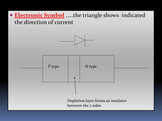
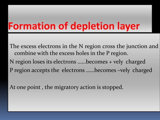
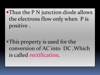
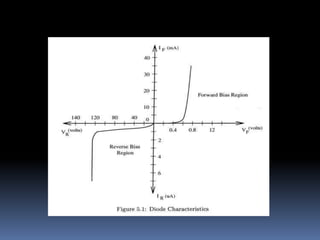
3. P-N JUNCTION :-A p–n junction is a
boundary or interface between two
types of semiconductor material, p-
type and n-type, inside a single crystal
of semiconductor. It is created by
doping.
4. Electronic Symbol …..the triangle shows indicated
the direction of current
Depletion layer forms an insulator
between the 2 sides
P type N type
5. Formation of depletion layer
The excess electrons in the N region cross the junction and
combine with the excess holes in the P region.
N region loses its electrons ……becomes + vely charged
P region accepts the electrons ……becomes –vely charged
At one point , the migratory action is stopped.
6. An additional electrons from the N region are repelled
by the net negative charge of the p region.
Similarly,
An additional holes from the P region are repelled by
the net positive charge of the n region.
Net result
a creation of a thin layer of each side of the junction
……….which is depleted (emptied) of mobile charge
carriers…. This is known as DEPLETION LAYER
..Thickness is of the order of 10-6meter.
7. The depletion layer contains no free and
mobile charge carriers but only fixed and
immobile ions.
Its width depends upon the doping level..
Heavy doped……..thin depletion layer
lightly doped……..thick depletion layer
8. POTENTIAL BARRIER
The electrons in the N region have to climb the potential
hill in order to reach the P region
Electrons trying to cross from the N region to P region
experience a retarding field of the battery and therefore
repelled. Similarly for holes from P region.
Potential thus produced are called ..potential barrier
Ge..0.3 V Si ..0.7V
9. PN junction can basically work in two modes, (A
battery is connected to the diode )
forward bias mode ( positive terminal
connected to p-region and negative terminal
connected to n region)
reverse bias mode ( negative terminal
connected to p-region and positive terminal
connected to n region) .
10. Forward biased PN junction
. It forces the majority charge carriers
to move across the junction
….decreasing the width of the
depletion layer.
11. Once the junction is crossed, a number of electrons
and the holes will recombine .
For each hole in the P section that combines with an
electron from the N section, a covalent bond breaks
and an electron is liberatyed which enters the positive
terminal
Thus creating an electron hole pair.
Current in the N region is carried by ….electrons
Current in the P region is carried by …. Holes.
12. Reverse biased PN junction
If the + of the battery is connected to the n-type and the
– terminal to the p-type,
the free electrons and free holes are
attracted back towards the battery, hence
back from the depletion layer, hence the
depletion layer grows.
Thus a reverse biased pn junction does not conduct
current.
13. Thus the P N junction diode allows
the electrons flow only when P is
positive .
This property is used for the
conversion of AC into DC ,Which
is called rectification.
16. APPLICATIONS-
….as rectifiers to convert AC into DC.
As an switch in computer circuits.
As detectors in radios to detect audio signals
As LED to emit different colours.