Stanley a Meyers analysis and test results of gated pulse frequency generator functional description
•
0 likes•244 views

Stanley a Meyers analysis and test results of gated pulse frequency generator functional description www.hot-rod-usa.com #hydrogen #hho #electronics #circuits

Recommended
Recommended
More Related Content
What's hot
What's hot (20)
Similar to Stanley a Meyers analysis and test results of gated pulse frequency generator functional description
Similar to Stanley a Meyers analysis and test results of gated pulse frequency generator functional description (20)
More from Daniel Donatelli
More from Daniel Donatelli (20)
Recently uploaded
Recently uploaded (10)
Stanley a Meyers analysis and test results of gated pulse frequency generator functional description
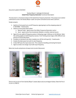
- 1. Global Open Source Project Written By Engineer Earl www.hot-rod-usa.com Document update 5/22/2019 Stanley Meyer’s Hydrogen On Demand Gated Pulse Frequency Generator Functional Description This document is a functional analysis of the Gated Pulse Frequency Generator. The purpose was to better understand its role in the Stanley Meyer’s water cell system and what function does it perform. Simple answers: 1. Switch on front panel turns on/off frequency signal going to cell by stopping output of IC SN7408N – Tested works 2. Switch on front panel select either: a. Manual mode - signal comes from Main Frequency Generator card or b. Accel - signal comes from Accelerator Module or another external source 3. Signal Pot sets width of frequency pulses in following range 3.102msec to 36.102msec. Note: this setting applies to both frequency sources. From Testing actual range a little different see pictures at end of document. 4. Provides an interface to let other modules turn off the cell Input (K) – Tested works 5. Creates the Gate wave train with its own frequency 6. It does NOT pass the input wave train. This is based on building and testing the board. 7. Signal out does not change much with input frequency. More test results and pictures of wave train at end of document. Picture and circuit are from Stanley Meyer’s estate above and circuit diagram below. Note the first 2 IC are in a 7402 IC.
- 2. Global Open Source Project Written By Engineer Earl www.hot-rod-usa.com Document update 5/22/2019 Inputs to card: 1. 5 VDC to drive the electronic (VDD) on circuit diagram 2. 10 VDC (VEE) to provide power to Green LED on front panel 3. Switch on front panel to turn Cell On/OFF 4. Pot 100 K ohms on front panel to adjust pulse width labeled L H. It’s the 100 K ohms pot (Labeled VIC GATING ADJ on circuit) 5. Switch on front panel to select Man Input (B) or Accel Input (M1) from other cards 6. Input (K) from Gas Feedback Control Module (Allows external module to shut off cell) 7. Fuse on ground to protect IC A26 (SN 74122N) value unknown. Outputs from card: 1. Gated signal (A) to VIC module (Does NOT include input wave train signal) 2. Gated signal to light the Green LED on panel No light no gate. 3. Test point on panel to allow viewing output signal Functional Description of Circuit The resisters and IC on the card are used to bias the ICs and will not be discussed with the exception of the 100K Pot. Other items will be covered left to right as input signal enters on left and leave on right with exception of input K which comes in as a bias from the top in top of the diagram Input (B) is from the Main Frequency Generator Board and is one of the 4 frequencies that are generated on that card.
- 3. Global Open Source Project Written By Engineer Earl www.hot-rod-usa.com Document update 5/22/2019 Input (M1) is from the Digital Control Means Module. For this analysis it is assumed input will be in the same range as can be provided from the Main Frequency Generator Board. The first two ICs on left are in a 7402 chip which contain 4 NOR logic gates only 2 are used. They are used in this circuit as and S-R Latch (Flip-Flop). See https://www.youtube.com/watch?v=mo4Lq0DvJ68 for good explanation of what they do as most data sheets do not explain why they are used. Simple explanation is they perform 2 functions 1) clean up the leading and training edges of the pulse to remove any noise in signal and 2) maintain the signal input at correct level for the SN74122N. NOTE as explained in the video NOR ICs can latch both the 0 and 1 states of the signal. Testing shows this only works correct when rest of circuit is functioning. Output locks up in low state if the pot sets the pulse width and frequency too low. There is a known lock up mode in a Flip-Flop used in this mode but when the rest of the circuit is working correctly this problem does not occur. I saw this problem in testing see test notes. IC SN74122N sets the size of pulse which is determined by the 100K Pot. This allows the size of the pulse width to be controlled from front panel 100K pot. From data sheet: Retriggerable Monostable Multivibrator Pin Function: An external timing capacitor may be connected between Cext and Rext/Cext. For accurate repeatable pulse widths connect an external resistor between Rext/Cext and Vcc leaving Rint open [unconnected]. To obtain variable pulse widths connect a variable resistance between Rint or Rext/Cext and Vcc. (This mode being used in circuit) The other resisters and capacitors around the chip set the bias conditions needed to support this function. Values shown in the circuit are selected to allow device to operate in this standard mode. The 1uF capacitor sets the formula that is required for this to be used do the calculation. I have included parts of the data sheet at end of this documents for reference. The equation we want is: Note: Be careful of units as equation expects input to have set exponents. Tw = 0.33 x Rt Cext Cext is 1uF or 1000000pF Rt = 4.7 + Pot + 4.7 So range is Low = 9.4 Center = 59.4 High =109.4 Tw low = 3,102,000ns or 3.102msec Tw center =19,802,000ns or 19.802msec Tw high = 36,102,000ns or 36.102msec
- 4. Global Open Source Project Written By Engineer Earl www.hot-rod-usa.com Document update 5/22/2019 Cell off switch on front panel when in off position sets the state of the final AND IC in SN7408N to LOW. When the output signal is LOW there are no pulses generated. The (K) Input is assumed to act like another switch input to turn cell off based on external events. As I have not reviewed function of that module, I have not verified that this is in fact the case, but testing shows if (K) goes low it does turn off output. Other drawings of this circuit do not show the (K) input so it appears it was added to support additional functions. I believe it may be used to turn cell off when pressure gets too high. Q11 2N3904 amplifies the output signal and feeds it to the following: 1. The Test Point on front panel 2. Lights the Green LED which also gets 10 VDC from an external source. I found that using 5 VDC lights the LED which pulses with signal. Pulse rate changes as the frequencies of the gate wave changes when pot is rotated. 3. Gate Signal (A) to the VIC Note: There are chips on the card that do not appear to be used by this circuit. Do not know why, it is possible that they supported a function no longer needed and card has not been updated. Just like the (K) input looks like it was added later.
- 5. Global Open Source Project Written By Engineer Earl www.hot-rod-usa.com Document update 5/22/2019 Details of SN72122N from data sheet
- 6. Global Open Source Project Written By Engineer Earl www.hot-rod-usa.com Document update 5/22/2019
- 7. Global Open Source Project Written By Engineer Earl www.hot-rod-usa.com Document update 5/22/2019
- 8. Global Open Source Project Written By Engineer Earl www.hot-rod-usa.com Document update 5/22/2019 Results of initial testing: 5/21/2019 Test setup: 1. Variable Frequency Generator (K2) board I built from Stanley’s circuit. This is now a bread board version where all the contacts are soldered. It is complete except for Frequency selector switches (I ordered wrong ones). For the testing I used jumper cables to select the frequencies from each of the 4 stages. Board had been tested earlier to verify it is functioning correctly. 2. Gated Pulse Frequency Generator (K3) board also built from a Stanley’s circuit diagram. The was in bread board plug in type. 3. 5 VDC output switching power supply which provide power to both boards. I also checked system with a 9 VDC battery which was only putting out 7 volts and got same results. 4. Rigol DS1052 Digital Oscilloscope 2 channel 50MHz 5. Various connector cables and jumpers. Initial tests and Results 1. Rechecked the Variable Frequency Generator Board (K2) to be sure it was working. a. Set Pot on board to generate 5KHz signal out of the 555 Timer b. Hooked up output signal to be 500Hz c. Verified the frequencies of the all 4 stages were: 5Khz, 500Hz, 50Hz and 5Hz. d. Did note change I had made to LED to connect it to ground instead of +5-volt seems to introduce some noise on signal. I will do more testing on this issue later, but it was small enough that it did not affect tests. e. Tested jumper connections to make sure I could select each of the frequency on output. Verified with O-scope. 2. Connected K3 board with jumper cable and the plugged-in power using jumpers from K2. Board K3 powered up and Green LED turned on and started pulsing. Checked with scope that I had a pulse wave train but did not pay much attention to it yet. 3. Decided to check the cell off switch function first used a jumper cable to pull pin to ground as I had not yet hooked up a switch. This worked and signal out went to flat line as expected. 4. I next check the (K) input. As I did not have (K) source I hooked input up +5V through 10K resister as that is how other inputs to AND were configured, that worked as signal was getting through. To test to see it does turn off the cell (output of the circuit), I disconnect the resister and that worked as expected and signal out went to flat line. However, when I plugged it back in signal did not come back. 5. Trouble shooting why no signal turns of I bumped the POT and it was loose in the circuit as it is on a plug-in board and pin where just plugged in. Plugged back in and still no output. I thought I may have blown something when I unplugged it as I did not have a signal in more coming out of the Flip-Flop when I check it. I spent several hours trying to get the Flip-Flop final output to generate a pulse. I disconnected everything and tested path through all the gates on chip and they all worked. Hooked things up using different combinations of the NORs same results. Checked the capacitor and it was OK. Try hooking it up without capacitor did not work. Neither
- 9. Global Open Source Project Written By Engineer Earl www.hot-rod-usa.com did swearing or yelling at it. Tried a different jumper cable to see if I had a bad plug-in connection and when I did that, I bumped the pot and green light blinked so I knew rest of
- 10. Global Open Source Project Written By Engineer Earl www.hot-rod-usa.com Document update 5/22/2019 circuit was OK though. Input using this connect was this flaky. Then I turned POT all the way to lowest setting and green light was pulsing again. I returned everything back to original configuration as light stayed pulsing and continued testing. a. What I have figured out. The down stream SN74122N must be working and when it is it provides feed back to the Flip-Flop (output of second stage also input to first stage) which then cause it to create a pulse on the output pin. This solves the know lockup problem with the Flip-Flop. While this is documented I did not expect the feedback. b. Also remembered that I had set the POT to zero when I started testing. When I reset the lose pot on the bread board, I had centered it and it turns on this was the real cause of the problem. Further testing show that the POT has a very narrow range of operation. Zero on POT to less than a quarter turn (more on signal later). When you go beyond that signal flat lines and the light goes out. I had done all the trouble shooting with pot in the center. This explains why there is a green light on board if it goes out there is no gate being generated. 6. Tests on signal output. a. At zero setting of POT (POT reads 0 when tested with ohm meter) you get the highest frequency pulse and the longest period. As you increase POT resistance in the POT the frequency goes down. Highest value was around 40Hz and it went to around 5Hz then signal flat lined and LED went off. Only took about a quarter turn on POT for this to happen. As the signal went down the LED pulsed slower. b. The Output signal was not what I expected. I had expected a 50 % pulse and that the board would change the width of the pulse. This is not the case. In fact, it appears this to a totally different wave train and it looks like this board generates the gate for the system. Adjusting the pot adjusts the size of the gate. See O-scope screen shots pictures below. c. Then tested effect of changing input frequency. As I was using the K2 board as my input source, I tested each of the 4 frequencies to see what would happen. Results surprised me the output changed very little. I included screen shots of this as well. 7. LED shows pulses when there is a pulse train available and is off when there is none. Note: I used the 5 VDC supply not 10 Volts show on circuit diagram. I assumed that new LEDs do not need the higher voltage and LED did work. What I do not know is the 10 volts on signal is need downstream. As this is a change to original circuit, I wanted to note this. 8. Conclusions so far: a. Board appears of function as designed and does what its names implies. It generates the gate wave train and that is only thing it does. b. The board output does not appear to be affected much by frequency of input. c. Gate frequency and period are adjusted by the POT d. As the frequencies generated by K2 do not pass through K3 I am not sure yet how it gets to VIC. There is a Q to K10 out of K2 labeled Water Injector in that circuit diagram, but I have not seen Q input on any of the circuit drawings I have. I have not seen an original drawing for the VIC.
- 11. Global Open Source Project Written By Engineer Earl www.hot-rod-usa.com e. I also notice that changing the POT on K2 is not a something you can do quickly because of the very small range and after each change you need to several seconds for signal to
- 12. Global Open Source Project Written By Engineer Earl www.hot-rod-usa.com Document update 5/22/2019 settle. It’s change pot setting, wait, look at scope and change it again. Very difficult to get a desire value. f. Did one last test, tried 50K ohm pot in place of the 100K could not get it to pulse at all. 9. At this point, I am satisfied enough with the initial test that I will move parts to a hardwired board and continue testing. O-Scope Pictures: This is near lowest frequency before signal disappears and lowest frequency for K2 at 5Hz. Notice Period and Freq values are at bottom on picture. Note: Pulse width and Frequency changes slightly at all settings so some of the difference you see in pictures is due to that but there is about 4ms change between lowest and high frequency on K2 2 Same setting on Gate board 50Hz on K2 Same Setting of Gate Board 500Hz on K2
- 13. Global Open Source Project Written By Engineer Earl www.hot-rod-usa.com Document update 5/22/2019 Same setting of Gate board 5KHz pulse on K2 Next set of pictures I have changed K2 to 500Hz and adjusted the POT on Gate board to show what changes Gate at 23Hz sorry for difference in screen size had to adjust scope to get signal on screen again. Watch how period changes with frequency as frequency goes up period goes down.
- 14. Global Open Source Project Written By Engineer Earl www.hot-rod-usa.com Document update 5/22/2019 This is the lowest setting on the K2 POT and the lowest period I only did a couple of these as adjustment is very touchy and you must wait after doing each one, as it take several seconds for signal to stabilize after moving POT. Big change initially, as you can see capacitors in circuit change state.