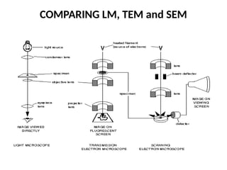
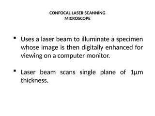
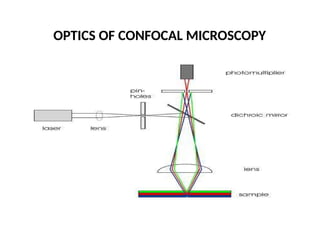
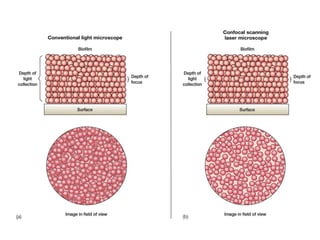
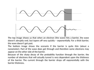
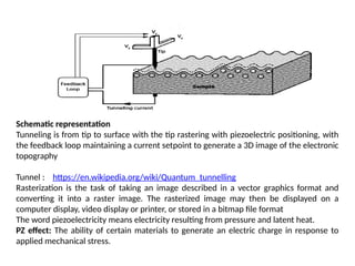
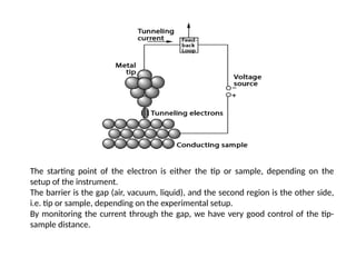
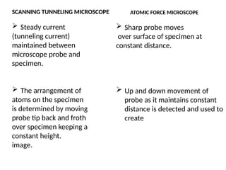
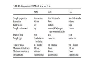
TEM SEM
Electron Beam Broad, static beams Beam focused to fine point;
sample is scanned line by line
Voltage Needed TEM voltage ranges from
60-300,000 volts
Accelerating voltage much lower;
not necessary to penetrate the
specimen
Interaction of the
electron beam
Specimen must be very thin Wide range of specimens
allowed; simplifies sample
preparation
Imaging Electrons must pass through and
be transmitted by the specimen
Information needed is
collected near the surface of the
specimen
Image Rendering Transmitted electrons are
collectively focused by the
objective lens and magnified to
create a real image
Beam is scanned along the
surface of the sample to
build up the image
COMPARING LM, TEM and SEM
CONFOCAL LASER SCANNING
MICROSCOPE
 Uses a laser beam to illuminate a specimen
whose image is then digitally enhanced for
viewing on a computer monitor.
 Laser beam scans single plane of 1μm
thickness.
OPTICS OF CONFOCAL MICROSCOPY
USES OF CONFOCAL MICROSCOPE
• Observing cellular morphology in
multilayered specimen.
Eg. used in diagnosing cervical cancer
• Evaluation and diagnosis of basal cell
carcinoma of skin.
ADVANTAGES OF A CONFOCAL
MICROSCOPE
• By using a confocal pinhole, the microscope is
really efficient at rejecting out of focus light so
that very thin section of a sample can be
analyzed.
• By scanning many thin sections through a
sample, one can build up a very clean three
dimensional image .
Scanning Probe Microscopes
 SPM are of a class of microscopes which use a
physical probe (a very small, very sharp needle)
which scan over the sample in contact or near-
contact with the surface.
 Used to visualize atoms and molecules.
 Two types:
• Scanning Tunneling Microscope (STM)
• Atomic Force Microscope (AFM)
SCANNING PROBE MICROSCOPES
Scanning probe microscopes
“feel” changes in surfaces of
the sample. They use ultrasharp
tips to measure changes in
electric currents, electrostatic
forces, or magnetic forces
coming from the surface.
The tips of the microscopes have to
be incredibly sharp to allow them
to collect information about
individual atoms or molecules.
 The development of the family of scanning
probe microscopes started with the original
invention of the Scanning Tunneling
Microscopy in 1981.
 Gerd Binnig and Heinrich Rohrer developed
the first working STM while working at IBM
Zurich Research Laboratories in Switzerland.
 Awarded Nobel prize in physics in 1986.
Working of Scanning Tunneling Microscope
The STM works by scanning a very sharp metal wire tip over a
surface. By bringing the tip very close to the surface, and by
applying an electrical voltage to the tip or sample, we can image
the surface at an extremely small scale – down to resolving
individual atoms.
The STM is based on several principles :
 One is the quantum mechanical effect of tunneling. It is this
effect that allows us to “see” the surface.
 Another principle is the piezoelectric effect. It is this effect
that allows us to precisely scan the tip with angstrom-level
control.
 Lastly, a feedback loop is required, which monitors the
tunneling current and coordinates the current and the
positioning of the tip.
Tunneling
Tunneling is a quantum mechanical effect. A tunneling current occurs
when electrons move through a barrier that they classically shouldn’t be
able to move through.
In classical terms, if you don’t have enough energy to move “over” a
barrier, you won’t. However, in the quantum mechanical world,
electrons have wavelike properties. These waves don’t end abruptly at a
wall or barrier, but taper off quickly. If the barrier is thin enough, the
probability function may extend into the next region, through the
barrier!
Because of the small probability of an electron being on the other side
of the barrier, given enough electrons, some will indeed move through
and appear on the other side. When an electron moves through the
barrier in this fashion, it is called tunneling.
Quantum mechanics tells us that electrons have both wave and particle-
like properties.
Tunneling is an effect of the wavelike nature.
The top image shows us that when an electron (the wave) hits a barrier, the wave
doesn’t abruptly end, but tapers off very quickly – exponentially. For a thick barrier,
the wave doesn’t get past.
The bottom image shows the scenario if the barrier is quite thin (about a
nanometer). Part of the wave does get through and therefore some electrons may
appear on the other side of the barrier.
Because of the sharp decay of the probability function through the barrier, the
number of electrons that will actually tunnel is very dependent upon the thickness
of the barrier. The current through the barrier drops off exponentially with the
barrier thickness.
Schematic representation
Tunneling is from tip to surface with the tip rastering with piezoelectric positioning, with
the feedback loop maintaining a current setpoint to generate a 3D image of the electronic
topography
Tunnel : https://en.wikipedia.org/wiki/Quantum_tunnelling
Rasterization is the task of taking an image described in a vector graphics format and
converting it into a raster image. The rasterized image may then be displayed on a
computer display, video display or printer, or stored in a bitmap file format
The word piezoelectricity means electricity resulting from pressure and latent heat.
PZ effect: The ability of certain materials to generate an electric charge in response to
applied mechanical stress.
The starting point of the electron is either the tip or sample, depending on the
setup of the instrument.
The barrier is the gap (air, vacuum, liquid), and the second region is the other side,
i.e. tip or sample, depending on the experimental setup.
By monitoring the current through the gap, we have very good control of the tip-
sample distance.
Piezoelectric Effect
The piezoelectric effect was discovered by Pierre Curie in 1880.
The effect is created by squeezing the sides of certain crystals, such as
quartz or barium titanate. The result is the creation of opposite charges on
the sides. The effect can be reversed as well; by applying a voltage across a
piezoelectric crystal, it will elongate or compress.
These materials are used to scan the tip in an STM and most other
scanning probe techniques.
A typical piezoelectric material used in scanning probe microscopy is PZT
(lead zirconium titanate).
Feedback Loop
Electronics are needed to measure the current, scan the tip,
and translate this information into a form that we can use for
STM imaging.
A feedback loop constantly monitors the tunneling current
and makes adjustments to the tip to maintain a constant
tunneling current. These adjustments are recorded by the
computer and presented as an image in the STM software.
Such a setup is called a constant current image.
In addition, for very flat surfaces, the feedback loop can be
turned off and only the current is displayed. This is a constant
height image
Atomic Force Microscopy
 Binnig, Quate, and Gerber invented the AFM in
1985.
 Developed to overcome a basic drawback with
STM – it can only image conducting or
semiconducting surfaces.
 The AFM has the advantage of imaging almost
any type of surface, including polymers,
ceramics, composites, glass, and biological
samples.
 Atomic force microscopy (AFM) to investigate
the electrically non-conductive materials, like
proteins.
Working of an Atomic Force Microscope
Analogous to how an Scanning Tunneling
Microscope works, a sharp tip is raster-scanned over
a surface using a feedback loop to adjust parameters
needed to image a surface.
Unlike STM, the AFM does not need a conducting
sample. Instead of using the quantum mechanical
effect of tunneling, atomic forces are used to map
the tip-sample interaction.
SCANNING TUNNELING MICROSCOPE
 Steady current
(tunneling current)
maintained between
microscope probe and
specimen.
 The arrangement of
atoms on the specimen
is determined by moving
probe tip back and froth
over specimen keeping a
constant height.
image.
ATOMIC FORCE MICROSCOPE
 Sharp probe moves
over surface of specimen at
constant distance.
 Up and down movement of
probe as it maintains constant
distance is detected and used to
create
microscopy contd....pptxiyd d h n SD s duos d

microscopy contd....pptxiyd d h n SD s duos d

  • 1.
    TEM SEM Electron BeamBroad, static beams Beam focused to fine point; sample is scanned line by line Voltage Needed TEM voltage ranges from 60-300,000 volts Accelerating voltage much lower; not necessary to penetrate the specimen Interaction of the electron beam Specimen must be very thin Wide range of specimens allowed; simplifies sample preparation Imaging Electrons must pass through and be transmitted by the specimen Information needed is collected near the surface of the specimen Image Rendering Transmitted electrons are collectively focused by the objective lens and magnified to create a real image Beam is scanned along the surface of the sample to build up the image
  • 2.
  • 3.
    CONFOCAL LASER SCANNING MICROSCOPE Uses a laser beam to illuminate a specimen whose image is then digitally enhanced for viewing on a computer monitor.  Laser beam scans single plane of 1μm thickness.
  • 4.
  • 6.
    USES OF CONFOCALMICROSCOPE • Observing cellular morphology in multilayered specimen. Eg. used in diagnosing cervical cancer • Evaluation and diagnosis of basal cell carcinoma of skin.
  • 7.
    ADVANTAGES OF ACONFOCAL MICROSCOPE • By using a confocal pinhole, the microscope is really efficient at rejecting out of focus light so that very thin section of a sample can be analyzed. • By scanning many thin sections through a sample, one can build up a very clean three dimensional image .
  • 8.
    Scanning Probe Microscopes SPM are of a class of microscopes which use a physical probe (a very small, very sharp needle) which scan over the sample in contact or near- contact with the surface.  Used to visualize atoms and molecules.  Two types: • Scanning Tunneling Microscope (STM) • Atomic Force Microscope (AFM)
  • 9.
    SCANNING PROBE MICROSCOPES Scanningprobe microscopes “feel” changes in surfaces of the sample. They use ultrasharp tips to measure changes in electric currents, electrostatic forces, or magnetic forces coming from the surface. The tips of the microscopes have to be incredibly sharp to allow them to collect information about individual atoms or molecules.
  • 10.
     The developmentof the family of scanning probe microscopes started with the original invention of the Scanning Tunneling Microscopy in 1981.  Gerd Binnig and Heinrich Rohrer developed the first working STM while working at IBM Zurich Research Laboratories in Switzerland.  Awarded Nobel prize in physics in 1986.
  • 11.
    Working of ScanningTunneling Microscope The STM works by scanning a very sharp metal wire tip over a surface. By bringing the tip very close to the surface, and by applying an electrical voltage to the tip or sample, we can image the surface at an extremely small scale – down to resolving individual atoms. The STM is based on several principles :  One is the quantum mechanical effect of tunneling. It is this effect that allows us to “see” the surface.  Another principle is the piezoelectric effect. It is this effect that allows us to precisely scan the tip with angstrom-level control.  Lastly, a feedback loop is required, which monitors the tunneling current and coordinates the current and the positioning of the tip.
  • 12.
    Tunneling Tunneling is aquantum mechanical effect. A tunneling current occurs when electrons move through a barrier that they classically shouldn’t be able to move through. In classical terms, if you don’t have enough energy to move “over” a barrier, you won’t. However, in the quantum mechanical world, electrons have wavelike properties. These waves don’t end abruptly at a wall or barrier, but taper off quickly. If the barrier is thin enough, the probability function may extend into the next region, through the barrier! Because of the small probability of an electron being on the other side of the barrier, given enough electrons, some will indeed move through and appear on the other side. When an electron moves through the barrier in this fashion, it is called tunneling. Quantum mechanics tells us that electrons have both wave and particle- like properties. Tunneling is an effect of the wavelike nature.
  • 13.
    The top imageshows us that when an electron (the wave) hits a barrier, the wave doesn’t abruptly end, but tapers off very quickly – exponentially. For a thick barrier, the wave doesn’t get past. The bottom image shows the scenario if the barrier is quite thin (about a nanometer). Part of the wave does get through and therefore some electrons may appear on the other side of the barrier. Because of the sharp decay of the probability function through the barrier, the number of electrons that will actually tunnel is very dependent upon the thickness of the barrier. The current through the barrier drops off exponentially with the barrier thickness.
  • 14.
    Schematic representation Tunneling isfrom tip to surface with the tip rastering with piezoelectric positioning, with the feedback loop maintaining a current setpoint to generate a 3D image of the electronic topography Tunnel : https://en.wikipedia.org/wiki/Quantum_tunnelling Rasterization is the task of taking an image described in a vector graphics format and converting it into a raster image. The rasterized image may then be displayed on a computer display, video display or printer, or stored in a bitmap file format The word piezoelectricity means electricity resulting from pressure and latent heat. PZ effect: The ability of certain materials to generate an electric charge in response to applied mechanical stress.
  • 15.
    The starting pointof the electron is either the tip or sample, depending on the setup of the instrument. The barrier is the gap (air, vacuum, liquid), and the second region is the other side, i.e. tip or sample, depending on the experimental setup. By monitoring the current through the gap, we have very good control of the tip- sample distance.
  • 16.
    Piezoelectric Effect The piezoelectriceffect was discovered by Pierre Curie in 1880. The effect is created by squeezing the sides of certain crystals, such as quartz or barium titanate. The result is the creation of opposite charges on the sides. The effect can be reversed as well; by applying a voltage across a piezoelectric crystal, it will elongate or compress. These materials are used to scan the tip in an STM and most other scanning probe techniques. A typical piezoelectric material used in scanning probe microscopy is PZT (lead zirconium titanate).
  • 17.
    Feedback Loop Electronics areneeded to measure the current, scan the tip, and translate this information into a form that we can use for STM imaging. A feedback loop constantly monitors the tunneling current and makes adjustments to the tip to maintain a constant tunneling current. These adjustments are recorded by the computer and presented as an image in the STM software. Such a setup is called a constant current image. In addition, for very flat surfaces, the feedback loop can be turned off and only the current is displayed. This is a constant height image
  • 18.
    Atomic Force Microscopy Binnig, Quate, and Gerber invented the AFM in 1985.  Developed to overcome a basic drawback with STM – it can only image conducting or semiconducting surfaces.  The AFM has the advantage of imaging almost any type of surface, including polymers, ceramics, composites, glass, and biological samples.  Atomic force microscopy (AFM) to investigate the electrically non-conductive materials, like proteins.
  • 19.
    Working of anAtomic Force Microscope Analogous to how an Scanning Tunneling Microscope works, a sharp tip is raster-scanned over a surface using a feedback loop to adjust parameters needed to image a surface. Unlike STM, the AFM does not need a conducting sample. Instead of using the quantum mechanical effect of tunneling, atomic forces are used to map the tip-sample interaction.
  • 21.
    SCANNING TUNNELING MICROSCOPE Steady current (tunneling current) maintained between microscope probe and specimen.  The arrangement of atoms on the specimen is determined by moving probe tip back and froth over specimen keeping a constant height. image. ATOMIC FORCE MICROSCOPE  Sharp probe moves over surface of specimen at constant distance.  Up and down movement of probe as it maintains constant distance is detected and used to create