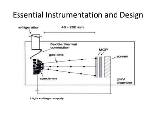
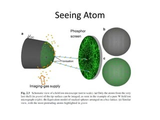
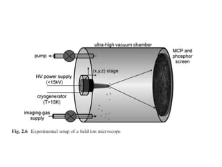
Atomic force microscope (AFM) is a scanning near-field tool for nanoscale investigation which was invented in 1986. Instead of using light or electron beam, AFM uses a sharp tip to ‘‘feel’’ samples. As the tip radius of curvature is on the order of nanometers, AFM can detect changes at a spatial resolution up to sub nanometer level. Compared to the optical microscope, AFM has a much higher spatial resolution which provides the ability to investigate ultrafine structure of samples and even map the distribution of single molecules.
As AFM utilizes direct contact between the tip and the sample, minimum or even no sample preparation is required.
Moreover, AFM can investigate samples in liquid which provides an opportunity to monitor samples close to their native surroundings. Further, AFM provides true 3D images. With optical and electron microscopies, only limited ranges in heights can be ‘‘in-focus’’ at any one time. Therefore, AFM can provide unique insight into the structure and functional behavior of materials. AFM is a versatile technique. Besides scanning the topography of a sample, it can also be used to investigate the mechanical properties of the sample as well as the interactions between the tip and the sample. AFM has been successfully applied in widespread branches of science and technology such as nanofabrication, material science, chemical and drug engineering, biotechnology and microbiology. As for above mentioned reasons, Atomic force microscope (AFM) is considered a useful tool for the nanoscale measurement in material-polymer science and engineering. AFM lacks the robust ability to chemically characterize materials.
Electron Microscopy - Scanning electron microscope, Transmission Electron Mic...Sumer Pankaj
An electron microscope is a microscope that uses a beam of accelerated electrons as a source of illumination. As the wavelength of an electron can be up to 100,000 times shorter than that of visible light photons, electron microscopes have a higher resolving power than light microscopes and can reveal the structure of smaller objects. A transmission electron microscope can achieve better than 50 pm resolution and magnifications of up to about 10,000,000x whereas most light microscopes are limited by diffraction to about 200 nm resolution and useful magnifications below 2000x.
Electron microscopes are used to investigate the ultrastructure of a wide range of biological and inorganic specimens including microorganisms, cells, large molecules, biopsy samples, metals, and crystals. Industrially, electron microscopes are often used for quality control and failure analysis. Modern electron microscopes produce electron micrographs using specialized digital cameras and frame grabbers to capture the image.
scanning electron microscope for analysisM Ali Mohsin
SEM stands for scanning electron microscope. The SEM is a microscope that uses electrons instead of light to form an image. Since their development in the early 1950's, scanning electron microscopes have developed new areas of study in the medical and physical science communities.
A Scanning Electron Microscope (SEM) is a powerful magnification tool that utilizes focused beams of electrons to obtain information. The high-resolution, three-dimensional images produced by SEMs provide topographical, morphological and compositional information makes them vital in science and industry.
3. Introduction
• It is a type of microscope that can be used to
image the arrangement of atoms at the
surface of a sharp metal tip.
• First Field ion microscope (FIM) was invented
by Müller in 1951.
• FIM, provides atomic-resolution imaging of
the surface of a specimen.
• FIM is a projection type microscope.
5. Basic principle
• FIM is differ considerably from those other of
optical and electron microscopy.
• Image is produce by the applying of high
voltage to the specimen with respect to the
channel plate screen.
• Required field strength at the sample surface
measure up to 50v/nm.
• Needle shape of specimen is prepared with
average radius of curvature 10-100nm.
6. • The electric field at the apex of the specimen is of
the order of 1010 V m–1.