
![14
Prof. V. K. Bairagi
• If the time interval is small, the failure rate is called-
Instantaneous Failure Rate. [F(t)] or “Hazard rate”. If
the time interval is long (such as total operational time)
the failure rate is called “Cumulative Failure Rate”.
• Mean Time Between Failures (MTBF)
– basic measure of reliability for repairable items.
– It can be described as the number of hours that
pass before a component, assembly, or system
fails.
– MTBF = (1,000,000 hours) / (2 failures) = 500,000
hours
Prof. V. K. Bairagi
Mean Time To Failure (MTTF)
• measure of reliability for non-repairable systems
• It is the mean time expected until the first failure of a
piece of equipment.
• Technically MTBF should be used only in
reference to repairable items, while MTTF should
be used for non-repairable items.
• However, MTBF is commonly used for both repairable
and non-repairable items.
n
1i
it
N
1
MTTF
ii
ii
n
1
MTTF
and
nrateFailureSystem
](https://image.slidesharecdn.com/epdupload-200805103058/75/Electronic-product-design-and-development-2-14-2048.jpg)


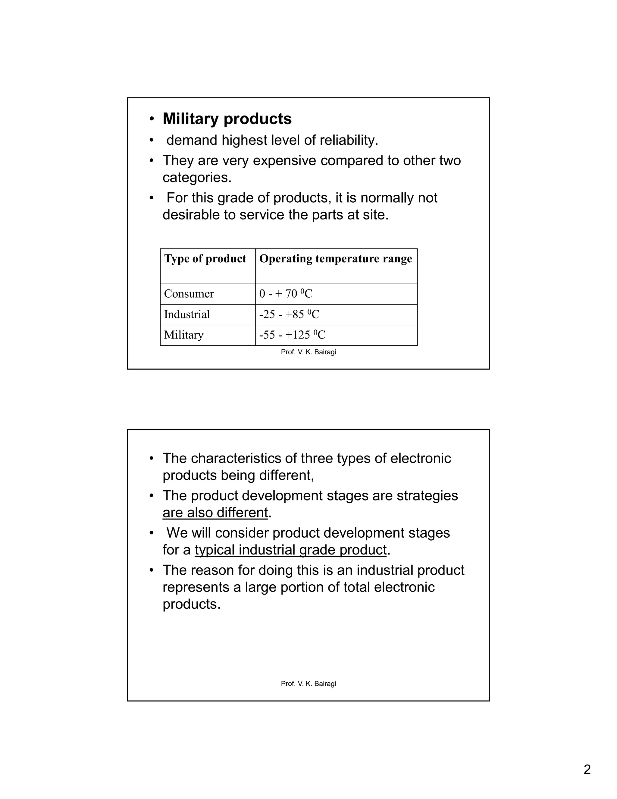
This document discusses different categories of electronic products and their characteristics. It describes consumer, industrial, and military products. Consumer products are low cost with fixed specifications and low reliability. Industrial products offer higher performance for specific applications and have higher costs and reliability requirements. Military products demand the highest reliability but are very expensive. The document then focuses on the stages of product development for an industrial grade product, including identifying customer requirements, assessing technical and commercial feasibility, designing, pilot production, testing, and quality assurance.


