This document discusses and compares the ISA, EISA, and microchannel bus architectures used in PCs. It notes that while ISA became a de facto standard, it has limitations like a narrow 16-bit bus and slow 8-bit DMA chips. EISA was developed as an evolutionary upgrade to ISA to allow 32-bit components while maintaining compatibility. The microchannel introduced by IBM is a revolutionary redesign but is proprietary. EISA aims to integrate both 16-bit and 32-bit components but ends up similar to ISA for 16-bit devices. Overall microchannel has a simpler design while EISA maintains compatibility with existing ISA devices and standards at the cost of greater complexity.
![558
Chapter 22 32-bit EISA Architecture - Evolution 559
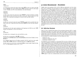
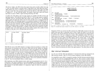
concerned. The address decoder on the expansion adapters then only decodes the low-order
address bytes further. Thus/ an ISA adapter which knows only a 10-bit I/O address can also be Register Call value Return walue
inserted into an EISA slot without any problems. AH cJ8h error code1)
2)
AL o1h/81h
CH function (0-n-1)
CL slot (0-63)
[E]SI offset info table 3) offset info tab!e 3)
DS segment info table 3)
segment info table 3)
Carry error if <> 0
With EISA adapter cards the IRQ used/ as well as the DMA channels, are programmable. The 1)
see Table 22.4.
configuration information Is stored in the extended CMOS RAM. EISA specifically extends the 2)
01h=CS with 16-bit addressing; 81h=CS with 32-bit addressing
CMOS RAM by 4 kbytes for this purpose. Special Installation programs provide support when 3)
information table:
configuring the EISA adapters, and automatically write data into the extended EISA CMOS Offset Size Entry
RAM. Typical information Is which I/O ports are used by the adapter, which IRQ and DMA OOh 2 words compressed ID (bits 0..1 and 13-15=character 2, bits 2..6=character 1, bit 7=reserved,
channels are assigned to the adapter, etc. This EISA system information can be retrieved by bits 8..12=character 3, bits 16-19, 20-23, 28-31=first, second and third digit of
means of several functions of INT 15h. They are listed In the following. product number, bits 24..27=revision number)
04h 1 word ID and slot info (bit 7 = 1 : multiple ID present, Bit 6: ID readable, bits 5..4: O0=slot,
01=embedded device, 10=virtual device, 11=reserved, bits 3..0: 0000=no multiple ID,
- INT 15h, Function d8h, Subfunction AL = OOh - Access to EISA System Information, lead 0001=first multiple ID,. . ., 1111=15th multiple ID, bit 8=1/0: EISA ENABLE supported/not
Slot Info supported, bit 9=1/0: EISA IOCHKERR supported/not supported, bits 1O..14=reserved,
bit 15=10: configuration incomplete/complete
06h 1 word revision number of configuration file
This function returns Information pertaining to the adapter In a certain slot.
08h 13 words select (byte O=first select, byte 1=second select, . . ., Byte 25=26th select)
22h 1 byte type of following function info (bit O=type/subtype, bit 1=memory, bit 2=interrupt,
bit 3=DMA, bit 4=port address area, bit 5=port initialization, bit 6=free entry,
Return walue bit 7=1/0: function disabled/enabled)
AH 23h 80 bytes type/subtype as ASCII string
d8h error code1)
AL 73h 63 bytes memory configuration (bit 0=1/0: RAM/ROM, bit 1=1/0: not cachable/cachable,
00h/80h2) vendor byte3)
BH bit 2=reserved, bit 3..4=memory type (00=system, 01=expanded, 10=virtual, 11=else),
utility revision (high)
BL bit 5=1/0: shared/non-shared memory, bit 6=reserved, bit 7=1/0=more entries/last entry,
utility revision (low)
CH bits 8..9=data access size (OO=byte, 01=word, 10=dword, 11 =reserved),
check sum configuration file (MSB) bits 10..11=decode size (00=20, 01=24, 10=32 bits, 1 Preserved), bits 12..15=reserved,
CL Slot (0-63) check sum configuration file (LSB)
DH bits 8-31=memory start address/1 OOh, bits 32-47=memory size/400h;
number of device functions max. eight identical 7-byte entries follow)
DL function information
SI:DI b2h 14 bytes interrupt configuration (bits O..3=interrupt no.. Oh..Ofh, bit 4=reserved, bit 5=1/0:
compressed vendor ID
Carry level/edge triggered, bit 6=1/0=shared/non-shared, bit 7=1/0: more entries/last entry;
error if <> 0
max. six identical 2-byte entries follow)
cOh 4 words DMA configuration (bits O..2=channel no. 0..7, bits 3-5=reserved, bit 6=1/0: shared/non-shared,
2) bit 7=1/0: more entries/last entry, bits 8..9=reserved, bits 10..11=transfer size (00=8,
00h=CS with 16-bit addressing; 80h=CS with 32-bit addressing
01=16, 10=32 bits, 11=reserved), bits 12..13=clocking (00=ISA compatible, O1=type A, 1O=type
•11=burst type C), bits 14..15=reserved; max. three identical 2-byte entries follow)
c8h 60 bytes I/O port info (bits 0..4=number of successive ports minus 1, bit 5=reserved, bit 6=1/0:
Bit 5..4: device/slot type (O0=slot, 01=embedded device, 10=virtual device, 11=reserved)
Bit 3..0: multinlp in (nnnn-™ ™,.I+:~I~ >^ ™«- - • multiple ID, shared/non-shared, bit 7=1/0: more entries/last entry, bits 8..23=port address;
multiple ID, 0001=first
max. 19 identical 3-byte entries follow)
104h 60 bytes initialization info (bits O..1=access type (00=byte, 01=word, 10=dword, 11=reserved), bit 2=1/0:
port write with/without mask, bits 3..6=reserved, bit 7—1/0: more entries/last entry, bits
8..23=port address;
INT 15h, Function d8h, Subfunction .
i - Access to EISA System Information, Read if bit 2=0 (no mask): byte 3 or bytes 3..4 or bytes 3..6=value;
Function Info if bit 2=1 (mask): byte 4 or bytes 5..6 or bytes 7..10=mask;
max. seven identical 4-byte, 5-byte, 7-byte or 11-byte entries follow)
This function returns 320 information bytes in an info table pertaining to the indicated function or after the first 115 bytes (free entry):
073h 205 bytes 205 free data bytes
in a certain slot. The calling program must provide a sufficiently large buffer for the info table.](https://image.slidesharecdn.com/eisa-100104082647-phpapp01/85/Eisa-6-320.jpg)
![560 Chapter 22 561
32-bit EISA Architecture - Evolution
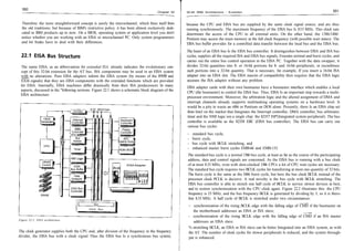
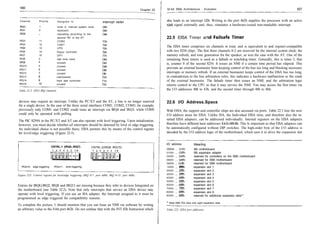
- INT 15h, Function d8h, Subfunction AL = 02h - Access to EISA System Information, Erase
Configuration RAM Error code Meaning
OOh no error
This function erases the CMOS RAM by writing a value of 0 to all addresses. invalid slot number
80h
81h invalid function number
Register Call value Return value 82h extended CMOS RAM damaged
83h slot doesn't contain any adapter
AH d8h error code1)
84h error upon writing into extended CMOS RAM
AL 02h/82h2)
85h CMOS RMA full
BH utility revision (high)
86h invalid BIOS call
BL utility revision (low)
87h invalid system configuration
Carry error if <> 0
1)
Table 22A: Error codes for INT 15h, function d8h
see Table 22.4
2)
02h=CS with 16-bit addressing; 88h=CS with 32-bit addressing
- INT 15h, Function d8h, Subfunction AL = 03h - Access to EISA System Information, Write
22.8 EISA Adapters and Automatic Configuration
Configuration
On EISA adapters you will look in vain for DIP switches, which sometimes made configuring
This function writes configuration values from a table of the calling program into the CMOS ISA adapters appear like gambling, with an unpredictable result. EISA solves the configuration
RAM. Additionally, a new checksum is calculated and written to the appropriate location, problem much more efficiently: every EISA adapter comes with a floppy disk holding a configu-
although you must also specify a correct value. The function must be called successively for ration file (CFG). The CFG stores the system elements of the EISA PC used, such as, for example,
every slot present in the system, even if no adapter is installed (the passed values must be set the assigned IRQ and DMA channels. This information is used by a configuration utility which
to 0). is delivered together with each EISA PC to configure both the adapter and PC correctly. Addi-
tionally, the utility is intelligent enough to detect access conflicts and to react appropriately.
Register Call value Return value Examples of this are address conflicts between two adapters whose address areas overlap, at
AH d8h error code1) least partially. This may occur with interfaces whose register addresses are equal, or with ident-
AL 03h ical ROM base addresses of the SCSI host and VGA graphics adapters. Such address conflicts
CX byte length of table are the main reason why an AT refuses to run after installing and configuring the brand-new
[E]SI offset of table2) VGA adapter.
DS segment of table2)
Carry error if <> 0 The CFG file was part of the EISA concept from the start. All the firms involved in EISA agreed
1)
to a standard for the file format, so incompatibilities do not arise here. The name of every CFG
see Table 22.4
2)
file must obey the following rule: fhhhpppp.CFG; where hhh is an abbreviation for the manu-
information table (the structure of the individual entries is the same as that of the information table of subfunction
01 h):
facturer, and pppp is a product identification. The CFG files themselves are pure ASCII files,
Size Entry and use a language with strictly defined commands that recall the CONFIG.SYS of MS-DOS.
2 words compressed ID Examples of CFG commands are: NAME = ???, SWT=???, BUSMASTER = value?, COMMENTS
1 word ID and slot info = text. Manufacturers can determine all the important parameters for their EISA adapters by
1 word revision number of configuration file using the CFG commands, so that the configuration utility need only read the CFG file to
1 word function length (this entry and the checksum do not contribute to the function length!)
2-26 bytes select
configure the EISA PC correctly with details of the newly Installed adapter. The user does not
1 byte type of function info need detailed knowledge of occupied addresses, DMA channels, etc. and the typical cow-at-a-
2-80 bytes type/subtype as ASCII string five-barred-gate feeling of untrained users can thus be avoided. The configuration data is stored
7-63 bytes memory configuration in the extended CMOS RAM, and the EISA PC boots without additional configuration next time.
2-14 bytes interrupt configuration If the configuration data in the CMOS RAM gets lost, for example, through a battery power-
1-4 words DMA configuration
3-60 bytes I/O port info
break, then you need simply start the configuration utility and reconfigure the system again
4-60 bytes initialization info using the CFG files for all installed adapters.
1 word checksum
or after the first 115 bytes (free entry):
Besides the CFG files, EISA has another concept for supporting configuration, the so-called
205 bytes 205 free data bytes overlay files (OVL). They supplement the configuration language on the level of the configuration
utility, and contain instructions In a format that looks like a mixture of C and Assembler. By](https://image.slidesharecdn.com/eisa-100104082647-phpapp01/85/Eisa-7-320.jpg)