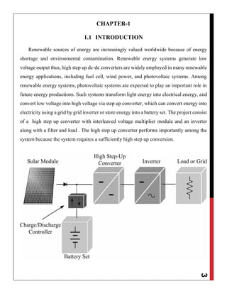
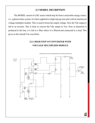
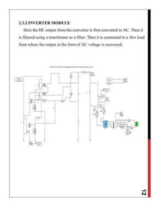
1. Submitted by:
EBBIN DANIEL
USF ID: U80380223
A HIGH STEP UP INTERLEAVED DC- DC CONVERTER WITH A
VOLTAGE MULTIPLIER MODULE FOR A PHOTOVOLTAIC
GRID SYSTEM
ENERGY DELIVERY SYSTEMS
PROJECT REPORT
ON
2. 1
ABSTRACT
A new high step up interleaved dc-dc converter with voltage multiplier for a
photovoltaic grid system is proposed in this project. Through a voltage multiplier module,
an asymmetrical interleaved high step up converter obtains high step up gain without
operating at an extreme duty ratio. The voltage multiplier module is composed of a
conventional boost converter and a boost converter. An extra conventional boost converter
is integrated into the first phase to achieve a considerably higher voltage conversion ratio.
The two phase configuration not only reduces the current stress through each power switch,
but also constrains the input current ripple, which decreases the conduction losses of metal
oxide semiconductor field effect transistors (MOSFETs).
In addition, the proposed converter functions as an active clamp circuit, which
alleviates large voltage spikes across the power switches. Thus the low voltage rated
MOSFETs can be adopted for reductions of conduction loss and cost. Efficiency increases
because the energy stored in leakage inductances is recycled to the output terminal. The
highest efficiency is 98%.
3. 2
CONTENTS
CHAPTER NO: TITLE PAGE NO
1 INTRODUCTION
1.1 Introduction 3
1.2 Existing system 4
1.3 Proposed system 5
2 PROJECT DESCRIPTION
2.1 block diagram 6
2.1.1 Block diagram description 6
2.2 System description
2.2.1 Boost converter 7
2.2.2 Voltage multiplier module 8
2.2.3 Inverter 9
2.3 Model description
2.3.1 High step up converter with 10
Voltage multiplier module
2.3.1.1 Specifications 11
2.3.1.2 Output 11
2.3.2 Inverter 12
2.3.2.1 Specifications 13
2.3.2.2 Output 13
3 CONCLUSION 14
4 REFERENCES 15
4. 3
CHAPTER-1
1.1 INTRODUCTION
Renewable sources of energy are increasingly valued worldwide because of energy
shortage and environmental contamination. Renewable energy systems generate low
voltage output thus, high step up dc-dc converters are widely employed in many renewable
energy applications, including fuel cell, wind power, and photovoltaic systems. Among
renewable energy systems, photovoltaic systems are expected to play an important role in
future energy productions. Such systems transform light energy into electrical energy, and
convert low voltage into high voltage via step up converter, which can convert energy into
electricity using a grid by grid inverter or store energy into a battery set. The project consist
of a high step up converter with interleaved voltage multiplier module and an inverter
along with a filter and load . The high step up converter performs importantly among the
system because the system requires a sufficiently high step up conversion.
5. 4
1.2 EXISTING SYSTEM
In the existing system, boost converters are used for step up process. The output
produced by the conventional system is less compared to the proposed system making it
less effective and less efficient.
Even the losses within the existing system makes it less efficient, thus generating less
output voltage.
Disadvantages:
1) Low output voltage
2) Leakage losses are high
3) Lower amount of efficiency
4) This system can be used for only low power applications
6. 5
1.3 PROPOSED SYSTEM
In the proposed system the voltage multiplier is combined with interleaved boost
converter to increase the output voltage. The coupled transformer is used to reduce the
cost. The leakage inductance will be recycled back to the transformer. When we give 40V
as input we can get 331V as an output. A conventional boost converter and two coupled
inductors are located in the voltage multiplier module, which stacks on a boost converter
to form an asymmetrical interleaved structure. The primary windings of a coupled
inductor with turns are employed to decrease input current ripple, and secondary
windings of the coupled inductor are connected in series to extend the voltage gain.
7. 6
CHAPTER 2
PROJECT DESCRIPTION
2.1 BLOCK DIAGRAM
2.1.1 BLOCK DIAGRAM DESCRIPTION
The block consist of a DC source which may be from a renewable energy source, i.e., a
photovoltaic system. It is then supplied to a high step up converter with an interleaved
voltage multiplier module. This is used to boost the output voltage. Now the Vdc output is
fed to an inverter. This is done to convert the Vdc output to Vac. Now as distortion is
produced in the line, it is fed to a filter where it is filtered and connected to a load. This
gives us the smooth Vac waveform.
8. 7
2.2 SYSTEM DESCRIPTION
2.2.1 BOOST CONVERTER
In electronics engineering, a DC to DC converter is a circuit which converts a
source of direct current from one voltage to another. It is a class of power converter. A
DC to DC converter is a device that accepts a DC input voltage and produces a DC
output voltage. Typically the output produced is at a different voltage level than the input.
In addition, DC to DC converters are used to provide noise isolation, power bus
regulation, etc. Such electronic devices often contain several sub circuits requiring a
unique voltage level different than that supplied by the battery. Additionally, the battery
declines as its stored power is drained. DC to DC converters offer a method of generating
multiple controlled voltages from a single variable battery voltage, thereby saving space
instead of using multiple batteries to supply different parts of the device.
Fig 2.3.7.1 simple circuit of boost converter
While the transistor is ON Vx=Vin, and the OFF state the inductor current flows
through the diode giving Vx=Vo. For this analysis it is assumed that the inductor current
always remains flowing. The voltage across the inductance and the average must be zero
for the average current to remain in steady state. Since the duty ratio ―D‖ is between 0
and 1 the output voltage must be higher than the input voltage in magnitude. The negative
sign indicates the reversal of the output voltage. A boost converter is a power converter
with an output DC voltage greater than its input DC voltage. It is a class of switching
9. 8
mode power supply containing at least two semiconductor switches and at least one
energy storage element.
2.2.2 VOLTAGE MULTIPLIER MODULE
A voltage multiplier is an electrical circuit that converts AC electrical power from a
lower voltage to a higher DC voltage, typically using a network of capacitors and diodes.
Voltage multipliers can be used to generate a few volts for electronic appliances, to
millions of volts for purposes such as high-energy physics experiments and lightning
safety testing. The most common type of voltage multiplier is the half-wave series
multiplier, also called the Villard cascade.
A voltage multiplier is an electronic circuit which charges capacitors from the input
voltage and switches these charges in such a way that, in the ideal case, exactly twice the
voltage is produced at the output as at its input.
10. 9
2.2.3 INVERTER
A power inverter, or inverter, is an electronic device or circuitry that changes direct
current (DC) to alternating current (AC). The input voltage output voltage and frequency,
and overall power handling depend on the design of the specific device or circuitry. The
inverter does not produce any power; the power is provided by the DC source.
A power inverter can be entirely electronic or may be a combination of mechanical
effects (such as a rotary apparatus) and electronic circuitry.
An inverter can produce a square wave, modified sine wave, pulsed sine wave, pulse
width modulated wave (PWM) or sine wave depending on circuit design. The two
dominant commercialized waveform types of inverters as of 2007 are modified sine wave
and sine wave.
There are two basic designs for producing household plug-in voltage from a lower-
voltage DC source, the first of which uses a switching boost converter to produce a
higher-voltage DC and then converts to AC. The second method converts DC to AC at
battery level and uses a line-frequency transformer to create the output voltage.
11. 10
2.3 MODEL DECRIPTION
The MODEL consist of a DC source which may be from a renewable energy source,
i.e., a photovoltaic system. It is then supplied to a high step up converter with an interleaved
voltage multiplier module. This is used to boost the output voltage. Now the Vdc output is
fed to an inverter. This is done to convert the Vdc output to Vac. Now as distortion is
produced in the line, it is fed to a filter where it is filtered and connected to a load. This
gives us the smooth Vac waveform.
2.3.1 HIGH STEP UP CONVERTER WITH
VOLTAGE MULTIPLIER MODULE
12. 11
This section is used to convert the low incoming DC voltage into stepped up DC
voltage. This is carried out by a high step up converter with a voltage multiplier module.
Its is seen that for an input voltage of 40 Vdc is converted to a 331Vdc.
2.3.1.1 SPECIFICATIONS
Switches used = MOSFET
Switching frequency for switch S1 and S2 = 40kHz
Magnetizing inductances (Lm1 and Lm2) = 133µH
Leakage inductances (Lk1 & Lk2) = 1.6µH
Turns ratio = Vp/Vs = 1
Capcitors : Cb , C2 , C3 = 220µH C1= 470µH
2.3.1.2 OUTPUT
For a 40V DC input, a 331V DC is obtained as an output.
13. 12
2.3.2 INVERTER MODULE
Here the DC output from the converter is first converted to AC. Then it
is filtered using a transformer as a filter. Then it is connected to a 1kw load
from where the output in the form of AC voltage is recovered.
14. 13
2.3.2.1 SPECIFICATIONS
Inverter used: IGBT 3 arm universal bridge.
Carrier frequency used for inverter = 1080 Hz
Modulating index (ma) = 0.85
Mode = discrete
Sampling time (Ts) = 5e-6
Filter used = transformer (delta –Y connected)
R L value of filter = 200Ω and 200H
Load used = 1kW
2.3.2.2 OUTPUT
15. 14
CHAPTER 3
CONCLUSION
A high step -up interleaved DC to DC boost converter with voltage multiplier module for
a photovoltaic grid system is proposed in this project. The proposed converter is applied to
boost up the voltage. The proposed converter has been successfully implemented in an
efficiently high step up conversion without an extreme duty ratio and number of turns ratios
through the voltage multiplier module with clamp feature.
The interleaved structure reduces the current that pass through the power switches and
reduces the input current ripple by approximately 6% . And here the leakage inductors are
present to recycle the leakage energy and sent back to the output terminal .
And due to the usage of coupled inductance the voltage stress on the power switch is
reduced We can select low voltage rating and low on-state resistance MOSFET and reduce
the overall design cost.
Thus an overall system was designed to produce maximum output voltage from any low
voltage DC producing source like a photovoltaic voltage source and thereby converting it
into AC with filtering process.
16. 15
CHAPTER 4
REFERENCES
A HIGH STEP-UP CONVERTER WITH A VOLTAGE
MULTIPLIER MODULE FOR A PHOTOVOLTAIC SYSTEM -
(IEEE TRANSACTIONS ON POWER ELECTRONICS, VOL. 28, NO. 6, JUNE 2013)
Kuo-Ching Tseng, Chi-Chih Huang, and Wei-Yuan Shih
VOLTAGE-SOURCED CONVERTERS IN POWER SYSTEMS
modeling, control, and applications - amirnaser yazdani, reza
iravani