Downloaded 11 times
![IOSR Journal of Electrical and Electronics Engineering (IOSR-JEEE)
e-ISSN: 2278-1676,p-ISSN: 2320-3331, Volume 5, Issue 4 (May. - Jun. 2013), PP 22-28
www.iosrjournals.org
www.iosrjournals.org 22 | Page
Solar Based Stand Alone High Performance Interleaved Boost
Converter with Zvs and Zcs
Ms.Nicy v.b1
, Mr.V.Karthikeyan2
1
(PG Scholar (EEE),Hindusthan college of Engineering and Technology, Coimbatore)
2
(Asst.professor(EEE),Hindusthan College of Engineering and Technology, Coimbatore)
Abstract: This paper introduces interleaved boost converters topology for PFC (power-factor-corrected),
which has continuous input current that you can manipulate with average-current-mode-control techniques to
force input current to track changes in line voltage. The concept of interleaving, or more generally that of
increasing the effective pulse frequency of any periodic power source by synchronizing several smaller sources
and operating them with relative phase shifts. With the help of the interleaving technology the inductor current
of interleaved boost converter can be reduced and thus inductor size is reduced. The Zero voltage technique
provides perfect turn on process of the converter . There is no overlap between the voltages and current, hence
no switching loss takes place at turn on process. The performance of proposed work is tested and verified by
MATLAB/SIMULINK software.
Keywords - interleaved boost converter, power factor correction (PFC), switching loss, zero-current
switching (ZCS), zero-voltage switching (ZVS).
I. INTRODUCTION
The power factor is defined as the ratio of the average power to the apparent power at an AC terminal.
When a converter has less than unity power factor means that the converter absorbs apparent power higher than
the real power consumes. This implies that the power source should be rated with higher VA ratings than the
load needs. In addition the current harmonics converter produces deteriorate the power source quality, which
affect the other equipment. The solution to improve the power factor is to add a passive filter, which is
composed of a capacitor and an inductor. However this passive filter is inefficient and bulky since it operates at
the line frequency. Therefore, thepower factor correction stage has to be inserted to the existing equipment to
achieve a good power factor. The PFC technique reduces current harmonics in utility systems produced by
nonlinear Load. Interleaved operation (the parallel connection of switching converters) of two or more boost
converters has been proposed to increase the output power and reduce the output ripple current [1]-[7]. This
technique consists of a phase shifting of the control signals of several cells in parallel operating at the same
switching frequency. As a result, the input and output current waveforms exhibit lower ripple amplitude. High-
switching-frequency operation is necessary to achieve small size of the converter. However, the switching loss
will increase as the switching frequency is increased. To solve these problem, soft switching techniques are
necessary. The zero-voltage-switched (ZVS) technique and zero-current-switched (ZCS) technique are two
commonly used soft switching methods. By adopting these ZCS and ZVS techniques, either voltage or current is
zero during switching transitions, which reduces the switching loss and also increases the reliability of the
power supplies. The choice of the soft-switching technique, i.e., ZCS(zero current source) or ZVS, it is taking
into account them technology of the semiconductor device will be used. For example, Power MOSFETSs
present a better performance when these are commutated under ZVS since they exhibit turn-on capacitive losses
when operating in ZCS increasing the switching losses and EMI. On the other, the IGBTs present better results
when are commutated under ZCS which can avoid their lath up and the turn-off losses caused by the tail current.
The ZCS techniques have some drawbacks such as a significant voltage stress on main diode, which increases
the conduction losses, and presence of the resonant inductor in series with the main switch, which increases the
magnetic losses. The technique of zero voltage switching is applicable to all switching topologies ZVS
technique [9]-[11]basically consists of forcing to zero the active switch voltage that prior to its turn-on by
creating a resonance between an inductor and a capacitor. The inductor also limits the rate of variation of the
diode current so losses due to the reverse recovery are reduced as well converter are simple topology, , fast
transient response,high power density and continuous input current. Therefore, the boost converters are usually
used in different power electronics applications such as active PFC, photovoltaic power systems and fuel cells.
Also interleaved operation (the parallel connection of switching converters) of two or more boost converters has
been proposed to increase the output power and to the reduce output ripple. This consists of a phase shifting of
the control signals of several cells in parallel operating at the same switching frequency. As a result, the input
and output current waveforms exhibit lower ripple amplitude.](https://image.slidesharecdn.com/d0542228-140503012435-phpapp01/85/Solar-Based-Stand-Alone-High-Performance-Interleaved-Boost-Converter-with-Zvs-and-Zcs-1-320.jpg)
![IOSR Journal of Electrical and Electronics Engineering (IOSR-JEEE)
e-ISSN: 2278-1676,p-ISSN: 2320-3331, Volume 5, Issue 4 (May. - Jun. 2013), PP 22-28
www.iosrjournals.org
www.iosrjournals.org 22 | Page
Solar Based Stand Alone High Performance Interleaved Boost
Converter with Zvs and Zcs
Ms.Nicy v.b1
, Mr.V.Karthikeyan2
1
(PG Scholar (EEE),Hindusthan college of Engineering and Technology, Coimbatore)
2
(Asst.professor(EEE),Hindusthan College of Engineering and Technology, Coimbatore)
Abstract: This paper introduces interleaved boost converters topology for PFC (power-factor-corrected),
which has continuous input current that you can manipulate with average-current-mode-control techniques to
force input current to track changes in line voltage. The concept of interleaving, or more generally that of
increasing the effective pulse frequency of any periodic power source by synchronizing several smaller sources
and operating them with relative phase shifts. With the help of the interleaving technology the inductor current
of interleaved boost converter can be reduced and thus inductor size is reduced. The Zero voltage technique
provides perfect turn on process of the converter . There is no overlap between the voltages and current, hence
no switching loss takes place at turn on process. The performance of proposed work is tested and verified by
MATLAB/SIMULINK software.
Keywords - interleaved boost converter, power factor correction (PFC), switching loss, zero-current
switching (ZCS), zero-voltage switching (ZVS).
I. INTRODUCTION
The power factor is defined as the ratio of the average power to the apparent power at an AC terminal.
When a converter has less than unity power factor means that the converter absorbs apparent power higher than
the real power consumes. This implies that the power source should be rated with higher VA ratings than the
load needs. In addition the current harmonics converter produces deteriorate the power source quality, which
affect the other equipment. The solution to improve the power factor is to add a passive filter, which is
composed of a capacitor and an inductor. However this passive filter is inefficient and bulky since it operates at
the line frequency. Therefore, thepower factor correction stage has to be inserted to the existing equipment to
achieve a good power factor. The PFC technique reduces current harmonics in utility systems produced by
nonlinear Load. Interleaved operation (the parallel connection of switching converters) of two or more boost
converters has been proposed to increase the output power and reduce the output ripple current [1]-[7]. This
technique consists of a phase shifting of the control signals of several cells in parallel operating at the same
switching frequency. As a result, the input and output current waveforms exhibit lower ripple amplitude. High-
switching-frequency operation is necessary to achieve small size of the converter. However, the switching loss
will increase as the switching frequency is increased. To solve these problem, soft switching techniques are
necessary. The zero-voltage-switched (ZVS) technique and zero-current-switched (ZCS) technique are two
commonly used soft switching methods. By adopting these ZCS and ZVS techniques, either voltage or current is
zero during switching transitions, which reduces the switching loss and also increases the reliability of the
power supplies. The choice of the soft-switching technique, i.e., ZCS(zero current source) or ZVS, it is taking
into account them technology of the semiconductor device will be used. For example, Power MOSFETSs
present a better performance when these are commutated under ZVS since they exhibit turn-on capacitive losses
when operating in ZCS increasing the switching losses and EMI. On the other, the IGBTs present better results
when are commutated under ZCS which can avoid their lath up and the turn-off losses caused by the tail current.
The ZCS techniques have some drawbacks such as a significant voltage stress on main diode, which increases
the conduction losses, and presence of the resonant inductor in series with the main switch, which increases the
magnetic losses. The technique of zero voltage switching is applicable to all switching topologies ZVS
technique [9]-[11]basically consists of forcing to zero the active switch voltage that prior to its turn-on by
creating a resonance between an inductor and a capacitor. The inductor also limits the rate of variation of the
diode current so losses due to the reverse recovery are reduced as well converter are simple topology, , fast
transient response,high power density and continuous input current. Therefore, the boost converters are usually
used in different power electronics applications such as active PFC, photovoltaic power systems and fuel cells.
Also interleaved operation (the parallel connection of switching converters) of two or more boost converters has
been proposed to increase the output power and to the reduce output ripple. This consists of a phase shifting of
the control signals of several cells in parallel operating at the same switching frequency. As a result, the input
and output current waveforms exhibit lower ripple amplitude.](https://image.slidesharecdn.com/d0542228-140503012435-phpapp01/75/Solar-Based-Stand-Alone-High-Performance-Interleaved-Boost-Converter-with-Zvs-and-Zcs-1-2048.jpg)
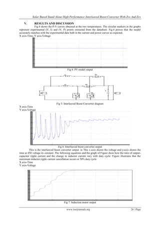
![Solar Based Stand Alone High Performance Interleaved Boost Converter With Zvs And Zcs
www.iosrjournals.org 27 | Page
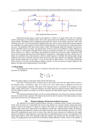
X axis-Time
Y axis-Voltage
Fig.8: PWM output for IGBT2
This is the PWM output for interleaved boost converter switches. The process of PWM
conversion is non-linear and it is generally supposed that low pass filter signal recovery is imperfect for PWM.
The PWM sampling theorem shows the PWM conversion can be perfect. The theorem states that any band
limited baseband signal within ±0.637 can be represented by a pulse width modulation (PWM) waveform with
unit amplitude. The number of pulses in this waveform is equal to the number of Nyquist samples and the peak
constraint is independent of whether the waveform is two-level or three-level.
VI. Conclusion
In this paper, a new interleaved boost PFC converter is proposed, which provides switching for the
power MOSFETs, through a circuit. This circuit provides reactive current during the transition times of the
MOSFETs [13]-[17] to charge and discharge the output capacitors of the MOSFETs. In addition, the control
system effectively optimizes the amount of reactive current required to achieve ZVS for the power MOSFETs.
The frequency loop, which is introduced in the control system, determines the frequency of the modulator based
on the load condition and the duty cycle of the converter. The experimental results and efficiency curves show
the superior performance of the proposed converter compared to the conventional one. The power factor
correction circuits were employed with PI controller to optimize the performance. So with this effect, the
converter module performs very well with the power factor as high as 0.93.
Acknowledgement
Authors would like to thank all the researchers who have contributed in this field of research. The comments
of anonymous reviewers to improve the quality of this paper are also acknowledged.
Reference
[1] R. Giral, L. Martinez-Salamero, and S. Singer, “Interleaved convertersoperation based on CMC,” IEEE Trans. Power Electron.,
vol. 14, no. 4,pp. 643–652, Jul. 1999.
[2] H. Kosai, S. McNeal, B. Jordan, J. Scofield, B. Ray, and Z. Turgut,“Coupled inductor characterization for a high performance
interleavedboost converter,” IEEE Trans. Magn., vol. 45, no. 10, pp. 4812–4815,Oct. 2009.
[3] C. A. Gallo, F. L. Tofoli, and J. A. C. Pinto, “A passive lossless snubberapplied to the AC–DC interleaved boost converter,” IEEE
Trans. PowerElectron., vol. 25, no. 3, pp. 775–785, Mar. 2010.
[4] Y. Jang and M. M. Jovanovic, “Interleaved boost converter with intrinsicvoltage-doubler characteristic for universal-line PFC front
end,” IEEETrans. Power Electron., vol. 22, no. 4, pp. 1394–1401, Jul. 2007.
[5] F. Musavi, W. Eberle, and W. G. Dunford, “A high-performance single-phasebridgeless interleaved PFC converter for plug-in
hybrid electricvehicle battery chargers,” IEEE Trans. Ind. Appl., vol. 47, no. 4, pp. 1833–1843, Jul./Aug. 2011.
[6] C. A. Gallo, F. L. Tofoli, and J. A. C. Pinto, “Two-stage isolated switch modepower supply with high efficiency and high input
power factor,”IEEE Trans. Ind. Electron., vol. 57, no. 11, pp. 3754–3766, Nov. 2010.
[7] M. O’Loughlin, “UCC28070 300-W interleaved PFC pre-regulator designreview,” TI Appl. Rep. SLUA479B, Aug. 2008, revised
Jul. 2010.
[8] C.-P. Ku, D. Chen, C.-S. Huang, and C.-Y. Liu, “A novel SFVM-M3control scheme for interleaved CCM/DCM boundary-mode
boost converterin PFC applications,” IEEE Trans. Power Electron., vol. 26, no. 8,pp. 2295–2303, Aug. 2011.2303, Aug. 2011.
[9] Y. T. Chen, S. M. Shiu, and R. H. Liang, “Analysis and design of a zero-voltage-switching and zero-current-switching interleaved
boost converter,”IEEE Trans. Power Electron., vol. 27, no. 1, pp. 161–173, 2011.
[10] G. Yao, A. Chen, and X. He, “Soft switching circuit for interleaved boost converters,” IEEE Trans. Power Electron., vol. 22, no. 1,
pp. 80–86, Jan.2007.
[11] B.-R. Lin, H.-K. Chiang, C.-Y. Tung, and C.-Y. Cheng, “Implementation of an interleaved ZVS boost-type converter,” in Proc.
IEEE Int. Symp.Ind. Electron., Jul. 5–8, 2009, pp. 819–824.
[12] N. Jain, P. Jain, and G. Joos, “A zero voltage transition boost converter employinga soft switching auxiliary circuit with reduced
conduction losses,”IEEE Trans. Power Electron., vol. 19, no. 1, pp. 130–139, Jan. 2004.](https://image.slidesharecdn.com/d0542228-140503012435-phpapp01/85/Solar-Based-Stand-Alone-High-Performance-Interleaved-Boost-Converter-with-Zvs-and-Zcs-6-320.jpg)
![Solar Based Stand Alone High Performance Interleaved Boost Converter With Zvs And Zcs
www.iosrjournals.org 28 | Page
[13] R. Streit and D. Tollik, “A high efficiency telecom rectifier using a novelsoft-switching boost-based input current shaper,” in
Proc.Conf. Rec. IEEEINTELEC, 1991, pp. 720–726.
[14] K. M. Smith and K. M. Smedley, “A comparison of voltage-mode softswitchingmethods for PWM converters,” IEEE Trans. Power
Electron.,vol. 12, no. 2, pp. 376–386, Mar. 1997.
[15] C.-J. Tseng and C.-L. Chen, “Novel ZVT-PWM converter with activesnubbers,” IEEE Trans. Power Electron., vol. 13, no. 5, pp.
861–869,Sep. 1998.
[16] G. Moschopoulos, P. Jain, G. Joos, and Y.-F Liu, “Zero voltage switchedPWMboost converter with an energy feed forward
auxiliary circuit,” IEEETrans. Power Electron., vol. 14, no. 4, pp. 653–662, Jul. 1999.
[17] T.-W. Kim, H.-S. Kim, and H.-W. Ahn, “An improved ZVT PWM boostconverter,” in Proc. Conf. Rec. IEEE Power Electron.
Spec. Conf., 2000,pp. 615–619.](https://image.slidesharecdn.com/d0542228-140503012435-phpapp01/85/Solar-Based-Stand-Alone-High-Performance-Interleaved-Boost-Converter-with-Zvs-and-Zcs-7-320.jpg)

This document summarizes a research paper on a solar-based interleaved boost converter with zero-voltage switching and zero-current switching. The converter uses two boost converters connected in parallel with a phase shift to reduce ripple and improve efficiency. Soft-switching techniques are used to reduce switching losses. Simulation results show the converter maintains a constant output voltage while the induction motor output varies with time, and PWM signals control the switches. The converter achieves a power factor of 0.93 and performs efficiently for power conversion from solar panels.


![[IJET- V2I2P17] Authors: Gaurav B. Patil., Paresh J. Shah](https://cdn.slidesharecdn.com/ss_thumbnails/ijet-v2i2p17-160609042055-thumbnail.jpg?width=640&height=640&fit=bounds)