The document describes a novel high-gain, high-power DC-DC converter topology for photovoltaic applications. The proposed converter consists of three interleaved boost converters with coupled inductors as the input inductors, along with two voltage multiplier cells. It is able to achieve a voltage gain of 10 and deliver 3kW of output power at 88% efficiency. The operating principle involves eight stages where the switches and diodes operate to transfer energy between the inductors and capacitors, providing high voltage gain while reducing voltage stress on the components. Simulation results validate the design concept and its advantages over existing solutions.


![High Gain High Power DC-DC Converter for
Photovoltaic Application
B.Sri Revathi
Research Scholar, School of Electrical Engineering
VIT University, Chennai Campus
Chennai, India
srirevathi.b@vit.ac.in
Dr.M.Prabhakar
Associate Professor, School of Electrical Engineering
VIT University, Chennai Campus
Chennai, India
prabhakar.m@vit.ac.in
Abstract— This paper introduces a novel high gain
DC-DC converter topology which can be used for photovoltaic
(PV) applications. The proposed DC-DC converter consists of 3
interleaved boost converters and 2 voltage multiplier cells
(VMC). The operating principle, characteristic waveforms,
design details along with the simulation results prove the validity
of the design and its superiority over existing converter topologies
in terms of its ability to provide high voltage gain at higher power
level and low device stress. The proposed topology is able to
produce a voltage gain of 10 and deliver 3kW output power at
88% efficiency.
Keywords—High gain, high power, interleaved boost converter,
voltage multiplier cell, PV systems
I. INTRODUCTION
Renewable Energy Sources (RES) are gradually gaining
importance in meeting the required electrical energy demand.
The output voltage from RES such as PV modules, fuel cells,
etc. is generally less. The normal practice is to use an input
supply in the range of 12V to PV 70V DC which is obtained
by series-parallel connection of modules. To meet the high
voltage gain requirement, conventional boost converters need
to be operated under extreme duty ratios. This causes severe
voltage stress across the power switches, diodes and
capacitors. By using transformer with suitable turns ratio, the
problem of extreme duty ratio operation can be alleviated [1],
[2]. Transformerless high gain DC-DC converters are
proposed as an alternative to the traditional solution due to
their higher operating efficiency, light weight and low cost [3].
Some of the existing transformer less high gain DC – DC
converter solutions include coupled inductor structures and /
or fly back topologies with charge pump, interleaved step-up
converter used in conjunction with a voltage multiplier cell,
multilevel switched capacitor DC-DC converter, etc.
In coupled inductor with switched capacitor topology,
operating at appropriate duty ratio yields high voltage gain.
Further, the voltage spikes across the main switch are clamped
[4]. So, switches with low ON state resistance can be
employed. Thereby the conduction loss reduces and efficiency
increases. But the number of components used is high and
output power is limited.
In [5], voltage multiplier cells (VMC) were used to obtain
higher voltage gain. However, the switch voltage stress in the
VMC based topologies is equal to the output voltage. Further,
a relatively larger duty ratio of 0.76 was used which resulted
in incremental losses due to reverse recovery problem.
Topologies with built-in transformer and VMC have large
voltage conversion ratio, minimum voltage stress across the
power device and reduced diode reverse recovery problem [6].
However, the number of diodes and capacitors used increases
as the gain increases. This makes the circuit complex and
expensive. Fly back converter with active clamping and
voltage multiplier can produce high gain by using transformer
as an interface [7]. However, the use of a transformer causes
additional losses in the converter. Coupled inductor and
voltage doubler based converters provide double the gain of a
conventional converter operating at same duty ratio [8].
However, usage of many circuit components results in
complex and expensive circuits. Further, voltage ringing
across the diodes and power switches are more prominent due
to the leakage inductance of the coupled inductor.
In [9], clamp mode converters were used to reduce the
power switch and the diode voltage stresses besides reducing
the reverse recovery problems. However, additional power
loss occurs in the clamping circuit. Though topologies with
combination of forward converter and voltage doubler can
offer features like modular structure, low voltage stress and
high voltage transfer ratio, an isolation transformer should be
used [10]. In [11], quadratic boost and coupled inductor were
cascaded to achieve high gain and low voltage stress across
the devices. However, the power rating of the converter is
limited. Interleaved boost converter gives high gain, low
voltage stress, high efficiency, low current ripple but it has a
poor switch utilization ratio and power loss across the
switches is high [12].
Interleaved boost converters coupled with VMC and
employing soft switching concept were discussed in [13]-[15].
These converters provided the required voltage gain with
acceptable switch stress, but for a lower power rating of 1kW.
In [16], a two stage based power conversion was presented for
a 1 kW application. Though power rating was on the higher
side, these converters provided a voltage gain of about 5 only.
In this paper, a high step up high power hybrid dc – dc
converter comprising of three interleaved boost converters with
978-1-4673-5149-2/13/$31.00 ©2013 IEEE
International Conference on Microelectronics, Communication and Renewable Energy (ICMiCR-2013)](https://image.slidesharecdn.com/revathi13-210512031203/85/Revathi-13-2-320.jpg)
![coupled inductors acting as the input side boost inductors is
presented. Two VMC stages are connected at the outside of the
coupled inductor. Voltage gain and power handling capacity is
enhanced because of this hybrid arrangement. The operating
principle, characteristic waveforms, design details and
simulation results of the converter are presented.
II. PROPOSED CONVERTER
The proposed converter is derived by combining high step
up interleaved converters, coupled inductors and voltage
multiplier cell. Figure 1 shows the power circuit diagram
which consists of three interleaved boost converters combined
with two voltage multiplier cells. The input inductor of the
interleaved boost converters is obtained from the coupled
inductors primary windings. In order to achieve high gain, the
secondary windings of the coupled inductors are connected in
series. Further, the secondary windings of coupled inductors
are coupled with two multiplier cells formed by capacitors
CM1, CM2, and diodes DM1 and DM2.
A. Operating Principle
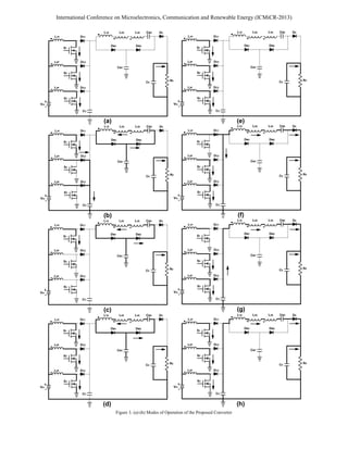
The proposed converter is assumed to be constructed using
ideal switches and diodes. Figure 2 shows the characteristic
waveforms of the proposed converter.
Stage 1 [t0, t1]:
The switches S1, S2 and S3 are in conduction state till t1. At
t1, gate pulses are removed to switches S2 and S3 and they are
turned OFF. The current through the inductors start to increase
linearly as in the case of a conventional boost converter. Since
all the diodes Dc1, Dc2 and Dc3 are in OFF state, the voltages
across them they will be clamped to VCc.
Stage 2 [t1, t2]:
At t1, S2 and S3 are turned OFF. Diodes DC2 and DC3
are turned ON. Also the multiplier diodes DM1 and DM2 turn
ON. Energy stored in the inductors L2P and L3P is transferred
to clamp capacitor Cc. Current through switch S1 increases and
current through clamp diodes DC2 and DC3 reduces when
current through DM1 and DM2 increase linearly.
Figure 1. Proposed converter circuit
Stage 3[t2, t3]:
At t2, current through L2P and L3P reduces. As a
result, the diodes DC2 and DC3 turn OFF naturally. So, diode
reverse recovery problems are alleviated. Further, current
through S1 is equal to current through L1P.
Stage 4[t3, t4]:
At t3, switches S2 and S3are turned ON by applying
gate pulses. This causes the current through the multiplier
diodes DM1 and DM2 to reduce. The current through L2P and
L3P increase linearly.
Stage 5[t4, t5]:
At t4, due to the discharging of stored energy in the
secondary side inductors, DM1 and DM2 turn OFF. Operation at
this stage is similar to stage 1.
Stage 6[t5, t6]:
At t5, S1 turns OFF and DC1 turns ON. Load is
connected to the input source through D0. L1S, L2S, L3S, CM1
and CM2 contribute to higher voltage gain with reduced switch
stress. Current through D0 is governed by the connected load.
Stage 7[t6, t7]:
At t6, current through L1 reduces to zero and DC1
turns OFF naturally. Current through S2 and S3 is the addition
of current through L1P, L2P and L3P.
Stage 8[t7, t0’]:
The circuit returns back to its original operating state
when S1 is turned ON. Current through D0 is limited by L1P,
L2P and L3P. The next cycle begins when the current through
D0 reduces to zero.
B. Analysis and Design Details
By using basic circuit theory concepts and applying
inductor volt-second balance, the voltage gain of the proposed
converter is found out. The voltage across the clamping
capacitor is given by
1
1
cc in
V V
D
=
−
(1)
When the switch S1 is ON, S2, S3 are OFF. Therefore,
L1P in L2P in cc L3P in cc
V V , V V V , V V V
= = − = − (2)
Figure 2. Characteristic waveforms during various modes of operation
International Conference on Microelectronics, Communication and Renewable Energy (ICMiCR-2013)](https://image.slidesharecdn.com/revathi13-210512031203/85/Revathi-13-3-320.jpg)
![The voltage across the multiplier capacitor is given by
CM2 L1S L2S L3S
V V V V
= + + (3)
When S1 is OFF, S2, S3 are ON. Therefore, the governing
equation is given by
cc L1S L2S L3S CM2 0
V V V V V V 0
− − − − − + = (4)
Rearranging equation (4) and substituting equation (1) gives
2
6
1
o in
V N V
D
⎛ ⎞
= −
⎜ ⎟
−
⎝ ⎠
(5)
It is observed from equation (5) that the coupled inductor turns
ratio (N) influences the voltage gain. Figure 4 shows the plot of
voltage gain plot for various duty cycle (D) and N.
From the plot, it is observed that depending on the voltage
gain requirements, the number of turns can be chosen based on
the operating duty cycle. It is preferred to obtain a voltage gain
of 10. Therefore, a plot which gives the various values of N
for a voltage gain of 10 is obtained as shown in Figure 5. It is
preferred to operate with a lesser number of turns based on the
following constraint.
1 2
6 3
N M
> + (6)
The design of multiplier capacitors (CM1, CM2) and the
clamp capacitor (Cc) depends on reducing the voltage ripple
across them. By considering the output power, operating
frequency and ripple voltage, the capacitor value is given by
Figure 4. Plot showing the relation between voltage gain (M), duty cycle (D)
and coupled inductor turns ratio (N).
Figure 5. Plot of turns ratio versus duty cycle to obtain a voltage gain of 10.
o
o C s
P
C
V V f
=
Δ
(7)
where C represents the value of multiplier or clamp capacitor,
Po is the output power, Vo is the output voltage, C
V
Δ is the
ripple voltage on the capacitors and fs is the switching
frequency. The value of the coupled inductor is determined
from the rate of fall of diode reverse recovery current. The
output diode has to withstand the output voltage. Hence, the
rate of fall of reverse recovery current is given by
1
o o
P
diD V
dt ML
= (8)
The values of L2P and L3P are made equal to L1P. Depending
on N, the values of L1S, L2S and L3S are computed.
III. SIMULATION RESULTS
The specifications of the proposed converter that was
simulated using PSpice are: input voltage = 24V, output
voltage = 230V, output power = 3kW, switching frequency =
100kHz. The duty cycle was chosen as 0.55 and the
corresponding N value was obtained as 2.4. The coupled
inductor values on the input side (L1P, L2P and L3P) were
chosen as 35µH. Based on N=2.4, the output side inductances
(L1S, L2S and L3S) were computed as 200µH. The multiplier
and the clamping capacitors (CM1, CM2 and Cc) were chosen to
be 47µF each. The load resistance was computed from the
output voltage and power. Figure 6 shows the output voltage
and output power waveforms. It is observed that the gate
pulses to switches S2 and S3 are applied after a delay. Further,
the output voltage and power matches with the theoretically
computed values. Figures 7(a)-(c) show the input side inductor
and the switch currents. The linear increase in inductor
currents during the application of a gate pulses can be
observed. As the switches are turned ON, the inductors and the
respective switches become series connected. Therefore, the
switch currents also exhibit the same behavior as that of the
inductor currents as long as they are turned ON. During turn
OFF state, as inductor stored energy is released to the load, the
inductor currents decrease and switch currents become zero.
To verify the design details of the power switches, the
simulated voltage and current stresses of each switch is shown
in Figures 8(a)-(c). It is observed that the peak voltage stress
across the device is almost equal to the output voltage. This is
within safe limits and as expected. Since the switches are
connected in the input side of coupled inductor and large
power transfer is involved, the current through the switches is
relatively large. However, due to practical availability of high
current rated devices, no problems are envisaged during
construction and testing of an experimental setup.
The voltage across the multiplier and the output
capacitors are shown in Figure 9. It is observed that the
capacitor voltage is slightly less than the output voltage. This
is in total agreement with the designed value obtained from
equation (7).
The enhanced power handling capability of the proposed
converter is depicted in Figure 10. It is observed that the
converter presented in [12] is able to deliver a load power of
International Conference on Microelectronics, Communication and Renewable Energy (ICMiCR-2013)](https://image.slidesharecdn.com/revathi13-210512031203/85/Revathi-13-5-320.jpg)
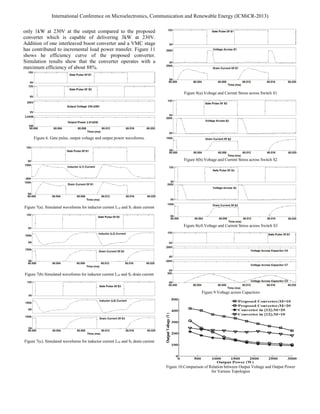
![Figure 11. Efficiency curve
IV. CONCLUSION
Existing DC-DC converter topologies provide high
voltage gain of about 10 but are not suitable for power
levels above 1kW. In this proposed converter, combining 3
interleaved boost converters with coupled inductors and
VMC combination high voltage gain at high power levels
are achieved. Further, the voltage stress on the power
devices used is low. Other advantages of the proposed
topology are its simple design and lesser number of
components compared to other existing topologies of similar
gain and power rating. Simulation results validate the ability
of the proposed converter to handle large power of about
3kW at a voltage gain of 10. Hence, this can be used in PV
applications due to its design simplicity, modular structure
and better performance.
REFERENCES
[1] A. Tomaszuk and A. Krupa, “High efficiency high step-up DC/DC
converters – a review”, Bulletin of Polish Academy of Sciences,
Technical Sciences, Vol. 59, No. 4, pp. 475 – 483, 2011.
[2] J. Dawidziuk, “Review and comparison of high efficiency high power
boost DC/DC converters for photovoltaic applications”, Bulletin of
the Polish Academy of Sciences,Technical Sciences, Vol. 59, No. 4,
pp. 499-506, 2011.
[3] David Meneses, Frede Blaabjerg, Oscar Garc´ıa, “Review and
Comparison of Step-Up Transformer less Topologies for Photovoltaic
AC-Module Application”, IEEE Transactions on Power Electronics,
Vol.28, No.6, pp. 2649-2663, June 2013.
[4] Wuhua Li, Xiaodong Lv, Yan Deng, Jun Liu, Xiangning He, “A
Review of Non-Isolated High Step-Up DC/DC Converters in
Photovoltaic Grid Connected Applications”, IEEE Transactions on
Industrial Electronics, Vol.58, No.4, pp.364-369, April 2011.
[5] Yi-Ping Hsieh, Jiann-Fuh Chen, Tsorng-Juu Liang and Lung-Sheng
Yang, “Novel High Step-Up DC–DC Converter with Coupled-
Inductor and Switched-Capacitor Techniques”, IEEE Transactions on
Industrial Electronics, Vol.59, No. 2, pp. 998 - 1007, February 2012.
[6] Marcos Prudente, Luciano L. Pfitscher, Gustavo Emmendoerfer,
Eduardo F. Romaneli and Roger Gules, “Voltage Multiplier Cells
Applied to Non-Isolated DC–DC Converters”, IEEE Transactions on
Power Electronics, Vol. 23, No. 2, pp. 871-887, March 2008.
[7] Yan Deng, Qiang Rong, Wuhua Li, Yi Zhao, Jianjiang Shi,
Xiangning He, “Single-Switch High Step-Up Converters With Built-
In Transformer Voltage Multiplier Cell”, IEEE Transactions on
Power Electronics, Vol. 27, No. 8, pp. 3557-3567, August 2012.
[8] Giorgio Spiazzi, Paolo Mattavelli and Alessandro Costabeber, “High
Step-Up Ratio Flyback Converter with Active Clamp and Voltage
Multiplier”, IEEE Transactions on Power Electronics, Vol. 26, No.
11, pp. 3205 -3214, November 2011.
[9] Lung-Sheng Yang, Tsorng-Juu Liang, Hau-Cheng Lee, and Jiann-Fuh
Chen, “Novel High Step-Up DC–DC Converter With Coupled-
Inductor and Voltage-Doubler Circuits”, IEEE Transactions on
Industrial Electronics, Vol. 58, No. 9, pp. 4196-4206, September
2011.
[10] Yi-Ping Hsieh, Jiann-Fuh Chen, Tsorng-Juu Liang, and Lung-Sheng
Yang, “A Novel High Step-Up DC–DC Converter for a Microgrid
System”, IEEE Transactions on Power Electronics, Vol.26, No. 4, pp.
1127-1136, April 2011.
[11] Ching-Ming Lai, Ching-Tsai Pan, and Ming-Chieh Cheng, “High-
Efficiency Modular High Step-Up Interleaved Boost Converter for
DC-Microgrid Applications”, IEEE Transactions on Industry
Applications, Vol. 48, No. 1,pp. 161 -171, January/February 2012.
[12] Shih-Ming Chen, Tsorng-Juu Liang, Lung-Sheng Yang, and Jiann-
Fuh Chen, “A Cascaded High Step-Up DC–DC Converter With
Single Switch for Microsource Applications”, IEEE Transactions on
Power Electronics, Vol. 26, No. 4, pp.1146 -1153, April 2011.
[13] Sungsik Park, Yohan Park, Sewan Choi, Woojin Choi, and Kyo-
Beum Lee, “Soft-Switched Interleaved Boost Converters for High
Step-Up and High-Power Applications”, IEEE Transactions on Power
Electronics, Vol.26, No. 10, pp. 2906 – 2914, October 2011.
[14] Wuhua Li, Yi Zhao, Yan Deng, and Xiangning He, “Interleaved
Converter With Voltage Multiplier Cell for High Step-Up and High-
Efficiency Conversion”, IEEE Transactions on Power Electronics,
Vol. 25, No. 9, pp. 2397-2408, September 2010.
[15] Kuo-Ching Tseng, Chi-Chih Huang, and Wei-Yuan Shih, “A High
Step-Up Converter with a Voltage Multiplier Module for a
Photovoltaic System”, IEEE Transactions on Power Electronics,
Vol.28, No. 6, pp. 3047-3057, June 2013.
[16] Rong-Jong Wai, Chung-You Lin, Chun-Yu Lin,Rou-Yong Duan, and
Yung-Ruei Chang, “High-Efficiency Power Conversion System for
Kilowatt-Level Stand-Alone Generation Unit With Low Input
Voltage”, IEEE Transactions on Industrial Electronics, Vol. 55,
No.10, pp. 3702 – 3714, October 2008.
International Conference on Microelectronics, Communication and Renewable Energy (ICMiCR-2013)
View publication stats
View publication stats](https://image.slidesharecdn.com/revathi13-210512031203/85/Revathi-13-7-320.jpg)


![[IJET V2I5P8] Authors: Lakshmi K R, Kavitha Issac, Kiran Boby](https://cdn.slidesharecdn.com/ss_thumbnails/ijet-v2i5p8-161107140749-thumbnail.jpg?width=640&height=640&fit=bounds)

![[IJET V2I5P9] Authors: Anju John Gray, Beena M Vargheese, Miss. Geethu James](https://cdn.slidesharecdn.com/ss_thumbnails/ijet-v2i5p9-161107141042-thumbnail.jpg?width=640&height=640&fit=bounds)