Download to read offline


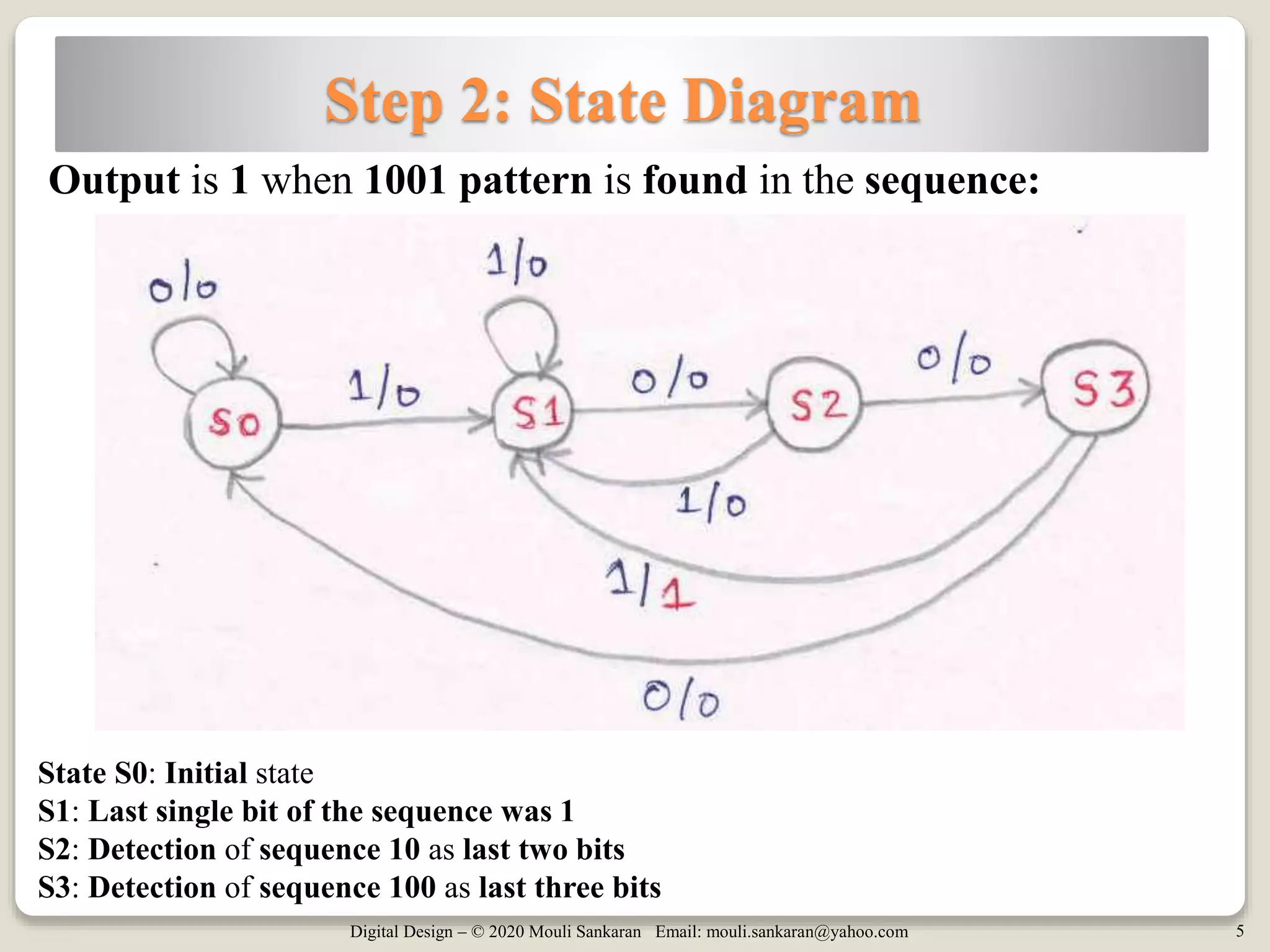


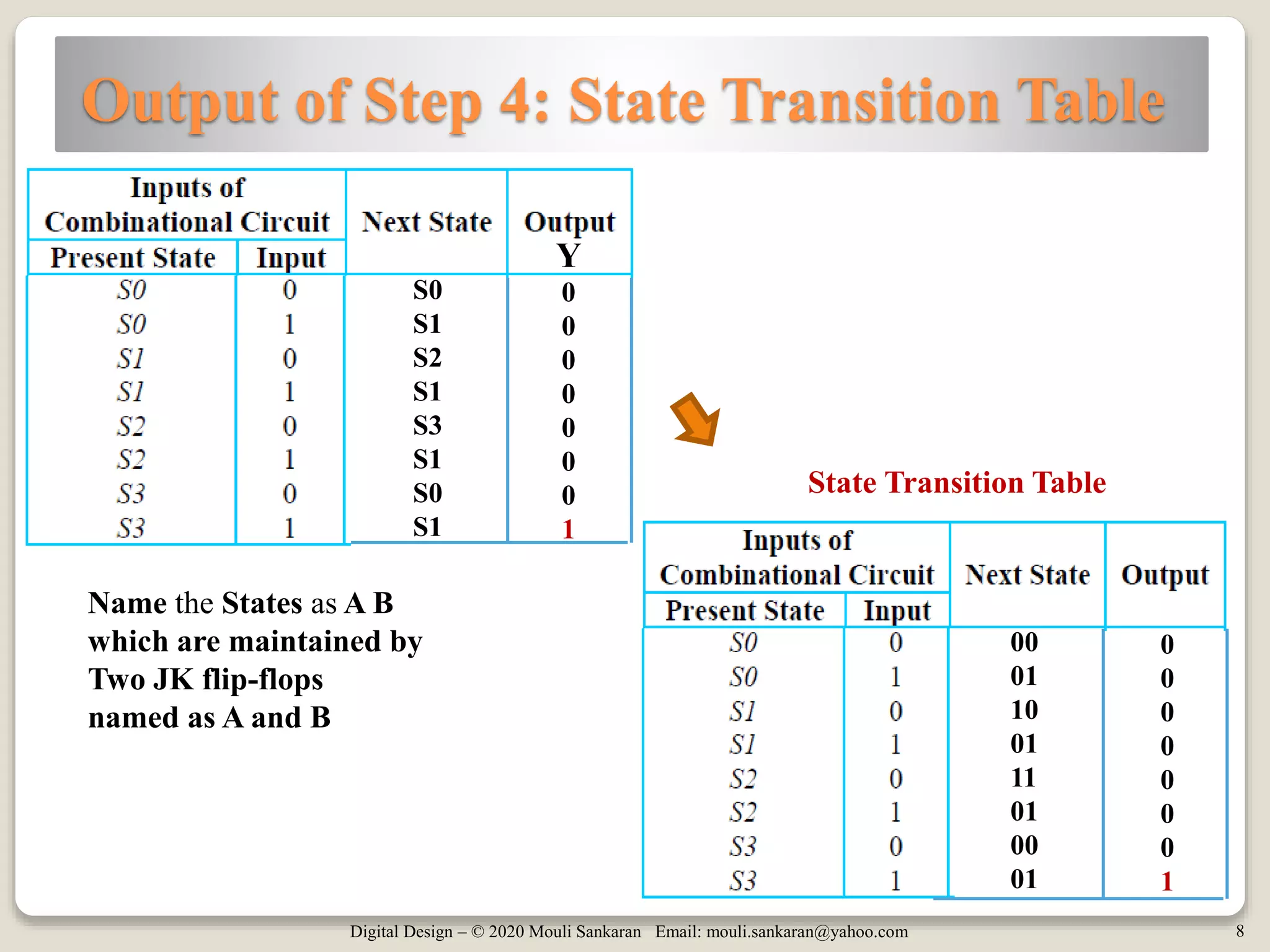


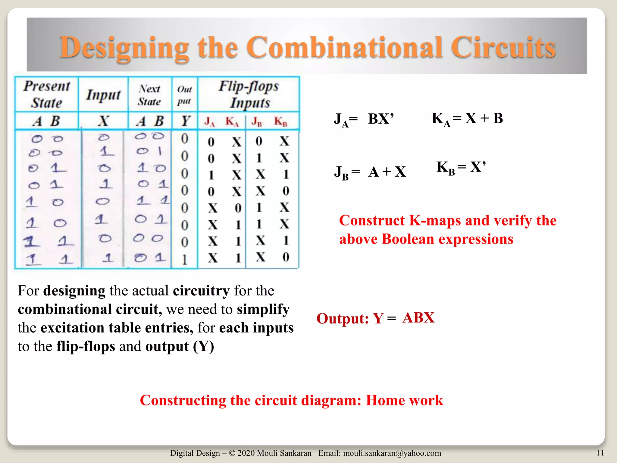

The document outlines the design of a sequence recognizer for the input sequence '1001' using JK flip-flops. It details the steps involved including problem definition, state diagram creation, state table generation, state assignments, and the design of combinational circuits. Additionally, it includes a summary and references for further study.