Download to read offline


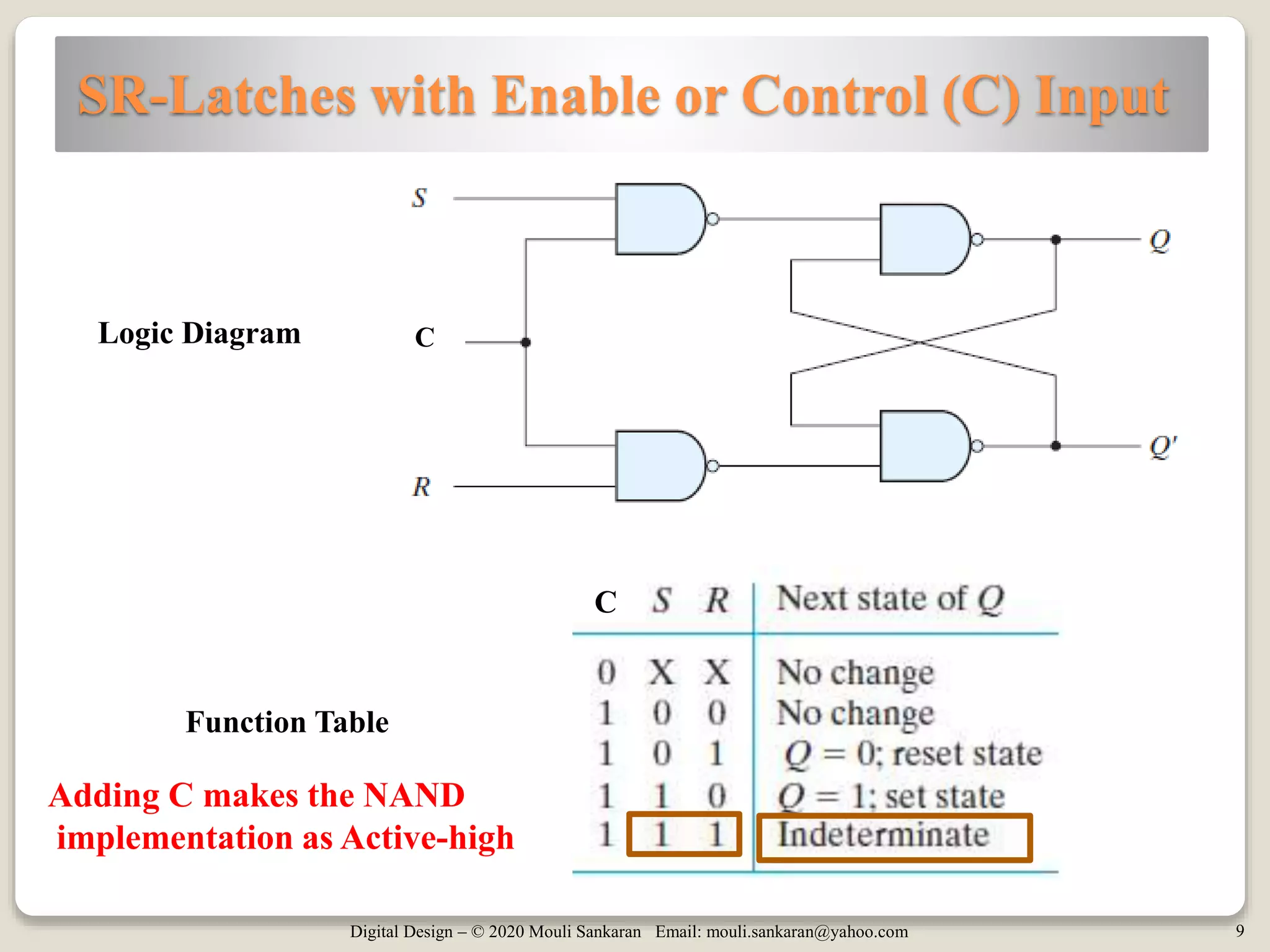


This document discusses different types of latches used as storage elements in digital circuits. It describes SR latches built using NOR gates that are active high, and S'R' latches built using NAND gates that are active low. D latches, also called transparent latches, are introduced which only have two inputs: data and control. The document explains issues with latches and concludes with the graphic symbols used to represent different latches in schematics.