Download to read offline

![International Research Journal of Engineering and Technology (IRJET) e-ISSN: 2395-0056
Volume: 09 Issue: 06 | June 2022 www.irjet.net p-ISSN: 2395-0072
© 2022, IRJET | Impact Factor value: 7.529 | ISO 9001:2008 Certified Journal | Page 990
The result analysis shows that MGDI technique shows
better results than the conventional CMOS logic in terms
of area.
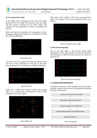
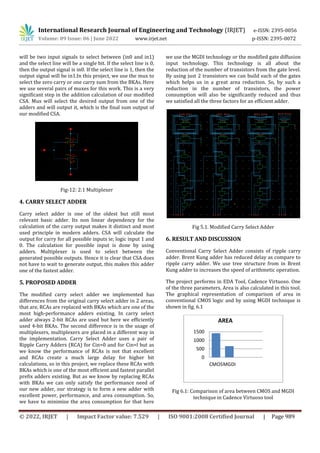
Power and delay is other design parameter. Power
consumption and delay of this circuit is calculated in
Cadence Virtuoso. . The graphical representation of
comparison of power consumption and delay in
conventional CSA and CSA with BKA is shown in fig 6.2.
The result analysis shows that CSA with BKA shows better
results than the conventional CSA in terms of Power
consumption and delay.
Fig 6.2: Comparison of power between CSA and modified
CSA in Cadence Virtuoso tool
Fig 6.3: Comparison of delay between CSA and modified
CSA in Cadence Virtuoso tool
6. CONCLUSIONS
IC design has always sought the best possible performance
on IC development in terms of speed, power consumption,
and area. This study paper found that incorporating the
MGDI technique in any design can reduce the area of the
circuit to a most satisfying extent. This work may also be
expanded to a larger number of bits. With the advent of
parallel prefix adder, the latency and power consumption
of various adder designs are lowered. Brent Kung adder is
chosen because parallel prefix adders produce quick
results. When compared to conventional CSA adder
architectures, the calculated results show that BKA Carry
Select Adder is better in terms of power consumption and
high speed, and can be used in various adder applications
such as multipliers, to execute different Digital Signal
Processing algorithms such as Finite Impulse Response,
Infinite Impulse Response, and so on.
REFERENCES
[1] Anas Zainal Abidin, Syed Abdul Mutalib Al Junid,
Khairul KhaiziMohd Sharif, Zulkifli Othman,
Muhammad AdibHaron “4-bit Brent Kung Parallel
Prefix Adder Simulation Study Using Silvaco EDA
Tools” DOI 10.5013/IJSSST
[2] Pappu P. Potdukhe, Vishal D. Jaiswal “Design of High
Speed Carry Select Adder Using Brent Kung Adder”
International Conference on Electrical, Electronics,
and Optimization Techniques (ICEEOT) – 2016
[3] G Tejaswini , V Jagannaveen , J V suman “Design of low
power ful adder using MGDI logic” European Journal
of Molecular & Clinical Medicine, ISSN 2515-8260
Volume 7, Issue 4, 2020
[4] Mr. Deepak Raj, Mrs. Sahana K Adyanthaya , Prof.
Praveen J, Prof. Raghavengra Rao R “Design and
Implementation of different types of efficient paral el
prefix adders” International Journal Of Innovative
Research In Electrical, Electronics, Instrumentation
And Control Engineering And National Conference on
advanced innovation in engineering and technology
(ncaiet-2015) alva’s institute of engineering and
technology, moodbidri vol. 3,special issue 1,april 2015
[5] P.B Natarajan, Samit Kumar Ghosh and R. Karthik “An
efficient carry select adder ” International Conference
on Electronics, Communication & Aerospace
Technology ICECA 2017
[6] Er. Aradhana Raju, Richi Patnaik, Ritto Kurian Babu,
PurabiMahato “Paral el Prefix Adders- A Comparative
Study For Fastest Response” 2016 International
Conference on Communication and Electronics
Systems, DOI: 10.1109/CESYS.2016.
[7] Basavoju Harish, Dr.K.Sivani, Dr.M.S.S.Rukmini
“Design and Performance Comparison among Various
types of Adder Topologies” Third International
Conference on Computing Methodologies and
Communication (ICCMC 2019)
25
17.83
CSA MODIFIED
CSA
POWER ( n watts)
4.584
3.73
CSA MODIFIED
CSA
DELAY (in µs )](https://image.slidesharecdn.com/irjet-v9i6168-221012101836-8aad4091/85/MODIFIED-CARRY-SELECT-ADDER-WITH-BKA-AND-MGDI-TECHNIQUE-5-320.jpg)

This document describes a modified carry select adder design using Brent Kung adder and modified gate diffusion input (MGDI) technique. The key modifications are: 1) Replacing the traditional ripple carry adders in carry select adders with faster Brent Kung adders to improve performance. 2) Using the MGDI technique to reduce the number of transistors in basic logic gates like AND, OR and XOR. This helps reduce the area and power consumption of the design. Simulation results show that the modified carry select adder has lower area, power consumption and delay compared to traditional carry select adder designs. By combining Brent Kung adder and MGDI technique, the design is able to achieve